EP0366413B1 - Fokussierungsdetektionsgerät - Google Patents
Fokussierungsdetektionsgerät Download PDFInfo
- Publication number
- EP0366413B1 EP0366413B1 EP89310948A EP89310948A EP0366413B1 EP 0366413 B1 EP0366413 B1 EP 0366413B1 EP 89310948 A EP89310948 A EP 89310948A EP 89310948 A EP89310948 A EP 89310948A EP 0366413 B1 EP0366413 B1 EP 0366413B1
- Authority
- EP
- European Patent Office
- Prior art keywords
- light
- accumulation
- light receiving
- light detector
- focus detection
- Prior art date
- Legal status (The legal status is an assumption and is not a legal conclusion. Google has not performed a legal analysis and makes no representation as to the accuracy of the status listed.)
- Expired - Lifetime
Links
Images



Classifications
-
- G—PHYSICS
- G02—OPTICS
- G02B—OPTICAL ELEMENTS, SYSTEMS OR APPARATUS
- G02B7/00—Mountings, adjusting means, or light-tight connections, for optical elements
- G02B7/28—Systems for automatic generation of focusing signals
- G02B7/34—Systems for automatic generation of focusing signals using different areas in a pupil plane
Definitions
- This invention relates to a focus detecting apparatus in an auto focus camera.
- a charge accumulation type light receiving element for example, a CCD image sensor
- a focus detecting apparatus in a camera.
- the illumination of the element surface varies from a high luminance to a low luminance depending on an object to be photographed and therefore, the accumulation time is varied and controlled so that the signal level to be processed becomes substantially constant.
- One of them is a method as disclosed, for example, in U.S. Patent No. 4,660,955 wherein the luminance of an object is monitored by a light receiving device differing from an image sensor and accumulation is terminated when the monitoring output reaches a predetermined level.
- US 4,618,235 discloses a variant of this method in which two integration time limits are provided. Integration is suspended when either the amount of light received by a monitor photo cell exceeds a predetermined value or a predetermined time elapses, whichever occurs first. Besides this method, there is also a method wherein charges are accumulated in advance in an image sensor for a certain time and after the termination of the accumulation, a signal from the image sensor itself is introduced and the next accumulation time is determined in conformity with the signal level.
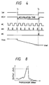
- the image sensor is a CCD or the like and therefore, it is difficult to individually detect a monitoring output corresponding to each light receiving element of the image sensor. As a result, it is unavoidable to monitor the average value of received light in a certain degree of range. If so, when as shown, for example, in Figure 8 of the accompanying drawings, there is an object of high luminance in the fashion of a spot, if monitoring is effected at the average value, there has been the problem that the peak value exceeds the dynamic range of signal processing and accurate focus detection calculation is impossible.
- a focus detection apparatus comprising: a first light detector having a plurality of light receiving elements receiving light from an area to be photographed; a second light detector positioned to receive light from said area to be photographed; processing means for providing a focus detection signal in dependence upon light received by said light receiving elements during an accumulation interval; characterised in that said processing means are so configured that at startup said accumulation interval is determined in accordance with the amount of light received by said second light detector and thereafter said interval is determined in accordance with light received by said light receiving elements during at least one preceding focus detection operation.
- Figure 1 schematically shows the construction of a first embodiment.
- Figure 2 shows the partial construction of the first embodiment.
- Figure 3 is a flow chart illustrating the operation of the first embodiment.
- Figure 4 is a timing chart illustrating the operation of the first embodiment.
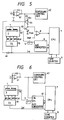
- Figure 5 schematically shows the construction of a second embodiment.
- Figure 6 schematically shows the construction of a third embodiment.
- Figure 7 is a flow chart showing a part of the operation of the present invention in detail.
- Figure 8 is a graph for illustrating disadvantages peculiar to the prior art.
- FIG. 1 shows an embodiment of the present invention.
- An object image is projected onto a charge accumulation type light receiving unit (CCD) 1 having a pair of one-dimensional image sensors by an imaging optical system not shown.
- a photodiode 2 putting out as a monitor output an output corresponding to the amount of exposure of the light receiving unit 1 is provided closely adjacent to the light receiving unit 1, and that output is input from a terminal Vmon to a buffer 4.
- An analog shift register 3 is disposed in contact with the light receiving unit 1.
- the outputs of the light receiving element of the light receiving unit 1 are successively put out as a time-serial signal from the terminal Vs of the analog shift register 3 after the termination of accumulation, and are input to an A/D converter 6 through a buffer 5.
- the outputs of the light receiving elements of the light receiving unit 1 converted into digital values by the A/D converter 6 are successively introduced into a CPU 7.
- the output of the buffer 4 is input to one input of a comparator 8.
- the other input of this comparator 8 is connected to a predetermined potential Vref, and the output of the comparator 8 is introduced into the CPU 7.
- the CPU 7 is connected also to a time counter 9, and is capable of clearing, starting and reading of the counted value of the time counter 9.
- the CPU 7 is connected to a timing generator (TG) 10 so as to be able to deliver the accumulation starting and terminating signal (INT) of the light receiving unit 1 to the timing generator (TG) 10.
- the timing generator (TG) 10 outputs a signal ⁇ INT regarding the accumulation, a signal ⁇ R regarding the reading-out, a transportation clock ⁇ C and a shift pulse ⁇ S so that the light receiving unit 1 can start and terminate the accumulation under the control of the CPU 7 and after the termination of the accumulation, the reading-out can be sequentially effected in the order of the shift of the accumulated charges to the shift register 3 and the transportation of the signal charge in the shift register 3.
- the detailed constructions of the output portions of the light receiving unit 1, the photodiode 2 and the shift register 3 are as shown in Figure 2.
- FIG. 3 shows the operation flow of the CPU, and description will be made in accordance therewith.
- the CPU 7 After the closing of the power source switch (step #1), the CPU 7 first judges whether the accumulate in the light receiving unit 1 for focus detection is the first accumulation after the closing of the power source switch (step #2), and if it is the first accumulation advance is made to step #3, and if it is not the first accumulation, skip is made to step #4.
- the time counter 9 is reset, and next, at step #5, the time counter 9 is started and the accumulation signal INT is set to "L", and the timing generator 10 is instructed to start the accumulation.
- step #6 it is detected that the output of the comparator 8 becomes "H".
- the timing generator 10 reports it to the light receiving unit 1, whereby the accumulating operation of the light receiving unit 1 is started.
- the resetting of the monitoring photodiode is released, and as shown in Figure 4, an output corresponding to the quantity of light impinging on the monitoring photodiode (in this example, the exposure amount from the start of the accumulaiton) is produced from the terminal Vmon.
- the output of the comparator 8 is designed to put out “L” until the exposure amount of the monitoring photodiode reaches a predetermined value, and to put out "H” when said exposure amount reaches said predetermined value.
- step #6 it is detected that the output of the comparator 8 becomes "H” and therfore, when the exposure amount of the monitoring photodiode reaches said predetermined value and the output of the comparator 8 beocmes "H", advance is immediately made to step #7, where the counting by the time counter 9 is stopped and the accumulation signal INT is set to "H".
- step #8 the time counter value is read and this is stored as the accumulation time in T.
- the timing generator as shown in Figure 4, shifts the accumulated charges to the analog shift register 3 and therefore, the shift pulse ⁇ S is given to the shift gate, thereby terminating the accumulation.
- the charges of the light receiving elements introduced into the analog shift register are successively output as light receiving element signals from the terminal Vs by the transportation clock ⁇ C.
- the light receiving element signals successively output from the terminal Vs by this transportation clock ⁇ C are A/D-converted at one light receiving element unit, and the CPU introduces thereinto these A/D-converted values in succession (step #9), and effects focus detection calculation by the use of this light receiving element data (step #10), and skip is again made to step #1.
- the maximum value Pmax of the outputs of the plurality of elements of the light receiving unit 1 is detected, and the details of this operation will be described later. In the second and subsequent accumulations, skip is made to step #4, where the next accumulation time is determined.
- the time counter is reset, whereafter the time counter 9 is started and the signal INT is set to "L", and the timing generator 10 is instructed to start the accumulation (step #12).
- step #13 the time counter value is read out and whether the counted value is equal to Tnext is judged, and if it is equal to Tnext, advance is made to step #15. If the counted value is not equal to Tnext, skip is made to step #13, where the reading-in of the time counter value is repeated.
- step #15 the timing generator 10 is instructed to terminate the accumulation with the accumulation signal INT as an "H" output, and at step #16, Tnext is stored in the accumulation time T for the calculation of the next accumulation time, and skip is made to step #9, where the A/D-converted values of the CCD data are successively introduced and focus detection calculation is effected (step #10), and skip is again made to step #2, where this sequence is repeated.
- FIG. 5 shows the construction of a focus detecting apparatus according to another embodiment, and in Figure 5, portions similar to those in Figure 1 are given similar reference numerals.
- a photometering circuit for controlling the exposure amount of film connected to a film exposure amount control circuit for determining the aperture value of a photo-taking lens and the speed of a shutter during the exposure of the film is diverted to a quantity-of-light detecting circuit.
- the output of a photometering amplifier 41 is input to a film exposure amount control circuit 42 and is also input to the base of a transistor 43.
- the collector of the transistor 43 is connected to the negative input terminal of the comparator 8 and is also connected to the other end of a capacitor 44 having one end thereof connected to a potential Vcc.
- the emitter of the transistor 43 is set to such an adjustable potential Vvar that the CCD light receiving element signal level becomes suitable.
- the capacitor 44 is capable of being short-circuited by a transistor 45.
- the accumulation signal output INT from the CPU 7 is "H" and therefore, the transistor 45 is turned on through an inverter 46 to short-circuit the capacitor.
- the transistor 45 is turned off and the capacitor 44 is gradually charged in conformity with the output of the photometering amplifier 41.
- the output of the comparator 8 becomes "H".
- the operation flow of the CPU 7 is similar to that of Figure 1 and therefore need not be described.
- the output of the photometering amplifier 41 is input to an A/D converter 61 to cause this A/D converter to process the output of the photometering amplifier.
- the first accumulation time after the closing of the power source switch is predetermined by the CPU 7 before the first accumulation on the basis of the A/D conversion value of the photometering amplifier 41.
- the second and subsequent accumulations, as in the previous embodiments, are found by calculation from the maximum value of the A/D-converted data and the accumulation time of the CCD at the last time. In the case of this embodiment, the comparator is unnecessary.
- the CPU 7 stores the output P1 of the first element of one of the pair of image sensors of the light receiving unit 1 into the internal memory thereof.
- the first element is shield from light so that no light may enter it.
- the content i of the internal counter of the CPU 7 is set to 2.
- whether the content of the internal counter is N+1 is judged.
- N corresponds to the number of the light receiving elements of one of the image sensors of the light receiving unit 1.
- the output P i of the i th light receiving element is stored into the internal memory.
- step #24 the output P i of the i th element is compared with the output P i-1 of the i-1 th element, and if the magnitude of P i is above the magnitude of P i-1 , the content of the internal memory P max is rewritten into P i at step #25.
- step #26 the content of the internal counter is incremented by 1. If at the step #22, the content of the internal counter becoems N+1, shift is made to the step #10 of Figure 7. Thereby, the peak value of the CCD is detected.
- the first accumulation time after the closing of the power source switch is controlled in conformity with the output of the quantity-of-light detecting circuit and therefore, irrespective of high luminance or low luminance, a substantially proper light receiving element signal level is obtained from the first time. Further, at the second and subsequent times, the next accumulation time is determined by calculation from the light receiving element signal level and the accumulation time and therefore, even in the case of an object to be photographed which has a special luminance distribution, focus detection can be accomplished reliably and the response of focus detection from after the closing of the power source switch can be made quick.
Landscapes
- Physics & Mathematics (AREA)
- General Physics & Mathematics (AREA)
- Optics & Photonics (AREA)
- Focusing (AREA)
- Automatic Focus Adjustment (AREA)
Claims (10)
- Fokusnachweisvorrichtung mit:
einem ersten Lichtdetektor (1), der eine Mehrzahl von Lichtaufnahmeelementen hat, die Licht von einem aufzunehmenden Gebiet empfangen,
einem zweiten Lichtdetektor (2), der so angeordnet ist, daß er Licht von dem aufzunehmenden Gebiet empfängt,
einer Verarbeitungseinrichtung (7) zum Bereitstellen eines Fokusnachweissignals in Abhängigkeit von dem durch die Lichtempfangselemente während eines Akkumulationsintervalls empfangenen Licht,
dadurch gekennzeichnet, daß
die Verarbeitungseinrichtung so konfiguriert ist, daß zu Beginn das Akkumulationsintervall in Übereinstimmung mit der durch den zweiten Lichtdetektor (2) empfangenen Lichtmenge bestimmt wird und danach das Intervall in Übereinstimmung mit dem durch die Lichtempfangselemente während mindestens eines vorangehenden Fokusnachweisvorganges empfangenen Licht bestimmt wird. - Vorrichtung nach Anspruch 1, wobei der erste Lichtdetektor (1) ein Lichtdetektor vom Ladungssammeltyp ist, in dem dessen Elemente Ladungen entsprechend der darauf auftreffenden Lichtmenge ansammeln.
- Vorrichtung nach Anspruch 1 oder Anspruch 2, die einen Zähler (9) zur Messung des Akkumulationsintervalls einschließt.
- Vorrichtung nach einem der Ansprüche 1 bis 3, wobei zu Beginn das Akkumulationsintervall durch Messung der Zeit bestimmt wird, die verstreicht, bis die durch den zweiten Lichtdetektor (2) empfangene Lichtmenge einen vorbestimmten Wert übersteigt.
- Vorrichtung nach einem der Ansprüche 1 bis 3, wobei zu Beginn das Akkumulationsintervall in Übereinstimmung mit der auf den zweiten Lichtdetektor (2) auftreffenden Lichtintensität zu Beginn des Fokusnachweisvorganges bestimmt wird.
- Vorrichtung nach einem der vorangehenden Ansprüche, wobei für einen Fokusnachweisvorgang nach dem Beginn die Akkumulationszeit durch Abwandlung einer vorherigen Akkumulationszeit in Abhängigkeit von dem durch die Lichtempfangselemente in einem vorherigen Schritt ausgegebenen Spitzenwert bestimmt wird.
- Vorrichtung nach Anspruch 6, wobei die vorherige Akkumulationszeit durch das Verhältnis aus dem Spitzenwertausgang durch ein Lichtempfangselement im vorherigen Schritt und dem Maximalwert, der durch das Lichtempfangselement ausgegeben werden kann, dividiert wird.
- Vorrichtung nach einem der vorangehenden Ansprüche, wobei der zweite Lichtdetektor eine Fotometerschaltung (41) zur Steuerung der Belichtung eines Films ist.
- Vorrichtung nach einem der vorangehenden Ansprüche, wobei der erste Lichtdetektor (1) zwei Anordnungen von CCD-Sensoren (1) aufweist.
- Vorrichtung nach Anspruch 9, wobei der zweite Lichtdetektor (2) auf demselben Halbleitersubstrat wie die CCD-Sensoren (1) gebildet und der zweite Lichtdetektor (2) eine fotoelektrische Wandlervorrichtung ist, die eine parallel zu den CCD-Anordnungen angeordnete Lichtempfangsfläche hat.
Applications Claiming Priority (2)
| Application Number | Priority Date | Filing Date | Title |
|---|---|---|---|
| JP267621/88 | 1988-10-24 | ||
| JP63267621A JP2893687B2 (ja) | 1988-10-24 | 1988-10-24 | 焦点検出装置 |
Publications (3)
| Publication Number | Publication Date |
|---|---|
| EP0366413A2 EP0366413A2 (de) | 1990-05-02 |
| EP0366413A3 EP0366413A3 (de) | 1991-07-31 |
| EP0366413B1 true EP0366413B1 (de) | 1995-04-12 |
Family
ID=17447235
Family Applications (1)
| Application Number | Title | Priority Date | Filing Date |
|---|---|---|---|
| EP89310948A Expired - Lifetime EP0366413B1 (de) | 1988-10-24 | 1989-10-24 | Fokussierungsdetektionsgerät |
Country Status (4)
| Country | Link |
|---|---|
| US (1) | US4931822A (de) |
| EP (1) | EP0366413B1 (de) |
| JP (1) | JP2893687B2 (de) |
| DE (1) | DE68922179T2 (de) |
Families Citing this family (10)
| Publication number | Priority date | Publication date | Assignee | Title |
|---|---|---|---|---|
| JP2911521B2 (ja) * | 1990-02-15 | 1999-06-23 | キヤノン株式会社 | センサ装置 |
| JP3093781B2 (ja) * | 1990-11-09 | 2000-10-03 | オリンパス光学工業株式会社 | 合焦位置検出装置 |
| JPH04181128A (ja) * | 1990-11-14 | 1992-06-29 | Olympus Optical Co Ltd | 測光装置 |
| US5526088A (en) * | 1992-03-05 | 1996-06-11 | Nikon Corporation | Focus detection device |
| JP3590806B2 (ja) * | 1994-09-07 | 2004-11-17 | 株式会社ニコン | イメージセンサーシステムおよび自動焦点検出装置 |
| GB2298331B (en) * | 1995-02-22 | 2000-02-16 | Asahi Optical Co Ltd | Distance measuring apparatus |
| JP3700219B2 (ja) * | 1995-11-08 | 2005-09-28 | 株式会社ニコン | 焦点検出装置、および焦点検出装置の調整方法 |
| JP3747497B2 (ja) * | 1995-12-13 | 2006-02-22 | 株式会社ニコン | 測光装置 |
| JP4788054B2 (ja) * | 2001-03-28 | 2011-10-05 | 株式会社ニコン | 焦点検出装置 |
| JP5917051B2 (ja) * | 2011-09-08 | 2016-05-11 | キヤノン株式会社 | 半導体装置 |
Family Cites Families (2)
| Publication number | Priority date | Publication date | Assignee | Title |
|---|---|---|---|---|
| US4660955A (en) * | 1983-11-08 | 1987-04-28 | Minolta Camera Kabushiki Kaisha | Focus condition detecting device for use in a camera |
| JPH0727102B2 (ja) * | 1984-07-16 | 1995-03-29 | ミノルタ株式会社 | カメラの自動焦点検出装置 |
-
1988
- 1988-10-24 JP JP63267621A patent/JP2893687B2/ja not_active Expired - Lifetime
-
1989
- 1989-10-19 US US07/424,177 patent/US4931822A/en not_active Expired - Lifetime
- 1989-10-24 EP EP89310948A patent/EP0366413B1/de not_active Expired - Lifetime
- 1989-10-24 DE DE68922179T patent/DE68922179T2/de not_active Expired - Lifetime
Also Published As
| Publication number | Publication date |
|---|---|
| DE68922179T2 (de) | 1995-11-16 |
| EP0366413A3 (de) | 1991-07-31 |
| EP0366413A2 (de) | 1990-05-02 |
| DE68922179D1 (de) | 1995-05-18 |
| JPH02113215A (ja) | 1990-04-25 |
| US4931822A (en) | 1990-06-05 |
| JP2893687B2 (ja) | 1999-05-24 |
Similar Documents
| Publication | Publication Date | Title |
|---|---|---|
| US4635126A (en) | Image pick-up system | |
| US4701626A (en) | Accumulation time adjusting device for photo-electric converter | |
| US4733264A (en) | Charge-coupled device for automatic focusing and camera shake detector using such charge-coupled device | |
| US4523101A (en) | Image scanning system with signal integration time control | |
| EP0366413B1 (de) | Fokussierungsdetektionsgerät | |
| JPH0245813B2 (de) | ||
| US4411505A (en) | Camera | |
| EP0495976A1 (de) | Autofokuschip mit referenzwertbestimmungsschaltung | |
| US4320946A (en) | Camera focus detecting device | |
| JP2002213946A (ja) | イメージ信号出力方法、イメージ信号出力装置、測距装置及び撮像装置 | |
| US4870441A (en) | Photoelectric conversion apparatus for focus detection | |
| JPH0672974B2 (ja) | カメラの焦点検出装置 | |
| JPH11205694A (ja) | 光電変換装置及び焦点検出装置 | |
| JP3397221B2 (ja) | 測光装置 | |
| US5028948A (en) | Photoelectric transducer apparatus for focus detection | |
| JP2001305422A (ja) | 測距装置 | |
| GB2047036A (en) | Focus detection device | |
| US4762987A (en) | Automatic focusing system with correlation-determined disabling | |
| US4293207A (en) | Camera focus detecting device | |
| JP3808912B2 (ja) | 焦点検出センサ装置 | |
| JP2746258B2 (ja) | 焦点検出装置 | |
| JP3132440B2 (ja) | 電荷蓄積型光電変換装置 | |
| JPH0731346B2 (ja) | カメラの手振れ検出装置 | |
| JP3013925B2 (ja) | デフォーカス量検出装置 | |
| JP2845859B2 (ja) | Ccd光量飽和制御回路 |
Legal Events
| Date | Code | Title | Description |
|---|---|---|---|
| PUAI | Public reference made under article 153(3) epc to a published international application that has entered the european phase |
Free format text: ORIGINAL CODE: 0009012 |
|
| AK | Designated contracting states |
Kind code of ref document: A2 Designated state(s): DE FR GB |
|
| PUAL | Search report despatched |
Free format text: ORIGINAL CODE: 0009013 |
|
| AK | Designated contracting states |
Kind code of ref document: A3 Designated state(s): DE FR GB |
|
| 17P | Request for examination filed |
Effective date: 19920123 |
|
| 17Q | First examination report despatched |
Effective date: 19931105 |
|
| GRAA | (expected) grant |
Free format text: ORIGINAL CODE: 0009210 |
|
| AK | Designated contracting states |
Kind code of ref document: B1 Designated state(s): DE FR GB |
|
| REF | Corresponds to: |
Ref document number: 68922179 Country of ref document: DE Date of ref document: 19950518 |
|
| ET | Fr: translation filed | ||
| PLBE | No opposition filed within time limit |
Free format text: ORIGINAL CODE: 0009261 |
|
| STAA | Information on the status of an ep patent application or granted ep patent |
Free format text: STATUS: NO OPPOSITION FILED WITHIN TIME LIMIT |
|
| 26N | No opposition filed | ||
| PGFP | Annual fee paid to national office [announced via postgrant information from national office to epo] |
Ref country code: FR Payment date: 19991011 Year of fee payment: 11 |
|
| PGFP | Annual fee paid to national office [announced via postgrant information from national office to epo] |
Ref country code: GB Payment date: 19991020 Year of fee payment: 11 |
|
| PG25 | Lapsed in a contracting state [announced via postgrant information from national office to epo] |
Ref country code: GB Free format text: LAPSE BECAUSE OF NON-PAYMENT OF DUE FEES Effective date: 20001024 |
|
| GBPC | Gb: european patent ceased through non-payment of renewal fee |
Effective date: 20001024 |
|
| PG25 | Lapsed in a contracting state [announced via postgrant information from national office to epo] |
Ref country code: FR Free format text: LAPSE BECAUSE OF NON-PAYMENT OF DUE FEES Effective date: 20010629 |
|
| REG | Reference to a national code |
Ref country code: FR Ref legal event code: ST |
|
| PGFP | Annual fee paid to national office [announced via postgrant information from national office to epo] |
Ref country code: DE Payment date: 20081016 Year of fee payment: 20 |