EP0366474B1 - Caméra à semi-conducteurs et appareil de mémoire à semi-conducteurs - Google Patents
Caméra à semi-conducteurs et appareil de mémoire à semi-conducteurs Download PDFInfo
- Publication number
- EP0366474B1 EP0366474B1 EP89311078A EP89311078A EP0366474B1 EP 0366474 B1 EP0366474 B1 EP 0366474B1 EP 89311078 A EP89311078 A EP 89311078A EP 89311078 A EP89311078 A EP 89311078A EP 0366474 B1 EP0366474 B1 EP 0366474B1
- Authority
- EP
- European Patent Office
- Prior art keywords
- camera
- solid state
- image storage
- storage means
- state image
- Prior art date
- Legal status (The legal status is an assumption and is not a legal conclusion. Google has not performed a legal analysis and makes no representation as to the accuracy of the status listed.)
- Expired - Lifetime
Links
- 239000007787 solid Substances 0.000 claims description 43
- 238000001514 detection method Methods 0.000 claims description 27
- 238000012546 transfer Methods 0.000 claims description 10
- 230000005055 memory storage Effects 0.000 claims description 8
- 238000004891 communication Methods 0.000 description 8
- 238000010586 diagram Methods 0.000 description 8
- 238000003780 insertion Methods 0.000 description 6
- 230000037431 insertion Effects 0.000 description 6
- 238000012545 processing Methods 0.000 description 4
- 230000002950 deficient Effects 0.000 description 3
- 230000003287 optical effect Effects 0.000 description 3
- 108010001267 Protein Subunits Proteins 0.000 description 2
- 230000004888 barrier function Effects 0.000 description 2
- 230000007547 defect Effects 0.000 description 2
- 239000004973 liquid crystal related substance Substances 0.000 description 2
- 238000012423 maintenance Methods 0.000 description 2
- 230000000007 visual effect Effects 0.000 description 2
- 229910021607 Silver chloride Inorganic materials 0.000 description 1
- 230000006835 compression Effects 0.000 description 1
- 238000007906 compression Methods 0.000 description 1
- 230000000994 depressogenic effect Effects 0.000 description 1
- 230000002401 inhibitory effect Effects 0.000 description 1
- 238000004519 manufacturing process Methods 0.000 description 1
- 229910052751 metal Inorganic materials 0.000 description 1
- 239000002184 metal Substances 0.000 description 1
- 238000000034 method Methods 0.000 description 1
- 230000004044 response Effects 0.000 description 1
- HKZLPVFGJNLROG-UHFFFAOYSA-M silver monochloride Chemical compound [Cl-].[Ag+] HKZLPVFGJNLROG-UHFFFAOYSA-M 0.000 description 1
Images


Classifications
-
- H—ELECTRICITY
- H04—ELECTRIC COMMUNICATION TECHNIQUE
- H04N—PICTORIAL COMMUNICATION, e.g. TELEVISION
- H04N1/00—Scanning, transmission or reproduction of documents or the like, e.g. facsimile transmission; Details thereof
- H04N1/21—Intermediate information storage
- H04N1/2104—Intermediate information storage for one or a few pictures
- H04N1/2112—Intermediate information storage for one or a few pictures using still video cameras
- H04N1/2137—Intermediate information storage for one or a few pictures using still video cameras with temporary storage before final recording, e.g. in a frame buffer
-
- H—ELECTRICITY
- H04—ELECTRIC COMMUNICATION TECHNIQUE
- H04N—PICTORIAL COMMUNICATION, e.g. TELEVISION
- H04N1/00—Scanning, transmission or reproduction of documents or the like, e.g. facsimile transmission; Details thereof
- H04N1/21—Intermediate information storage
- H04N1/2104—Intermediate information storage for one or a few pictures
- H04N1/2112—Intermediate information storage for one or a few pictures using still video cameras
-
- H—ELECTRICITY
- H04—ELECTRIC COMMUNICATION TECHNIQUE
- H04N—PICTORIAL COMMUNICATION, e.g. TELEVISION
- H04N1/00—Scanning, transmission or reproduction of documents or the like, e.g. facsimile transmission; Details thereof
- H04N1/21—Intermediate information storage
- H04N1/2104—Intermediate information storage for one or a few pictures
- H04N1/2158—Intermediate information storage for one or a few pictures using a detachable storage unit
-
- H—ELECTRICITY
- H04—ELECTRIC COMMUNICATION TECHNIQUE
- H04N—PICTORIAL COMMUNICATION, e.g. TELEVISION
- H04N23/00—Cameras or camera modules comprising electronic image sensors; Control thereof
-
- H—ELECTRICITY
- H04—ELECTRIC COMMUNICATION TECHNIQUE
- H04N—PICTORIAL COMMUNICATION, e.g. TELEVISION
- H04N5/00—Details of television systems
- H04N5/76—Television signal recording
- H04N5/765—Interface circuits between an apparatus for recording and another apparatus
- H04N5/77—Interface circuits between an apparatus for recording and another apparatus between a recording apparatus and a television camera
- H04N5/772—Interface circuits between an apparatus for recording and another apparatus between a recording apparatus and a television camera the recording apparatus and the television camera being placed in the same enclosure
-
- H—ELECTRICITY
- H04—ELECTRIC COMMUNICATION TECHNIQUE
- H04N—PICTORIAL COMMUNICATION, e.g. TELEVISION
- H04N2101/00—Still video cameras
-
- H—ELECTRICITY
- H04—ELECTRIC COMMUNICATION TECHNIQUE
- H04N—PICTORIAL COMMUNICATION, e.g. TELEVISION
- H04N2201/00—Indexing scheme relating to scanning, transmission or reproduction of documents or the like, and to details thereof
- H04N2201/21—Intermediate information storage
- H04N2201/214—Checking or indicating the storage space
-
- H—ELECTRICITY
- H04—ELECTRIC COMMUNICATION TECHNIQUE
- H04N—PICTORIAL COMMUNICATION, e.g. TELEVISION
- H04N5/00—Details of television systems
- H04N5/76—Television signal recording
- H04N5/907—Television signal recording using static stores, e.g. storage tubes or semiconductor memories
-
- Y—GENERAL TAGGING OF NEW TECHNOLOGICAL DEVELOPMENTS; GENERAL TAGGING OF CROSS-SECTIONAL TECHNOLOGIES SPANNING OVER SEVERAL SECTIONS OF THE IPC; TECHNICAL SUBJECTS COVERED BY FORMER USPC CROSS-REFERENCE ART COLLECTIONS [XRACs] AND DIGESTS
- Y10—TECHNICAL SUBJECTS COVERED BY FORMER USPC
- Y10S—TECHNICAL SUBJECTS COVERED BY FORMER USPC CROSS-REFERENCE ART COLLECTIONS [XRACs] AND DIGESTS
- Y10S358/00—Facsimile and static presentation processing
- Y10S358/906—Hand-held camera with recorder in a single unit
Definitions
- the present invention relates to a solid-state camera for use with detachable solid-state image storage means as a recording medium for a photographed image and a detachable solid-state image storage means for use therewith.
- An electronic still camera using a memory not requiring a movable mechanism for recording/reproduction of information (to be referred to as a solid-state camera hereinafter) has attracted attention as a successor of a silver chloride still camera and a video floppy electronic still camera.
- a solid-state camera In an electronic still camera, instantaneous reproduction of a photographed image, image transfer, computer image processing, electronic image filing and the like can be easily performed by electronically processing image information.
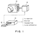
- Fig. 1 shows an arrangement of a solid-state camera system.
- a memory cartridge 12 as a solid-state memory apparatus for storing image information can be detached from a camera main body 10 of the solid-state camera.
- a reproducing apparatus 14 reproduces stored information in the memory cartridge 12.
- the memory cartridge 12 comprises, e.g., an IC memory device, a memory controller, and a backup power source therefor.
- an SRAM, a DRAM, an EPROM, an EEPROM, or the like is used.
- the memory cartridge 12 and the camera main body 10 are connected by using, e.g., a metal connector, a transmit coil, or a photocoupler.
- An image photographed by the camera main body 10 is stored in a predetermined format by the memory cartridge 12.
- the memory cartridge 12 By connecting the memory cartridge 12 to the reproducing apparatus 14 to reproduce the stored image, electronic image data can be transmitted from the reproducing apparatus to a TV monitor, a printer, a transmitter, a filing apparatus, and the like.
- the camera main body 10 must include a power source for driving various signal processors and exposure control means such as a lens driving means and an aperture driving means.
- a user therefore, must perform a maintenance operation for, e.g., checking the voltage of a power source battery of the camera main body 10 or replacing the battery before he or she uses the camera, resulting in a very cumbersome operation for a user.
- a maintenance operation for, e.g., checking the voltage of a power source battery of the camera main body 10 or replacing the battery before he or she uses the camera, resulting in a very cumbersome operation for a user.
- a write speed (or time) of the IC memory device in the memory cartridge 12 largely changes in accordance with the type of device. Therefore, as the memory capacity is increased, a difference between write times is increased.
- the size, connecting pins, and the like of the solid-state memory apparatus such as the memory cartridge 12 must be standardised.
- United States Patent No. 4837628 discloses a solid state camera which is designed to receive a memory card solid state image store. Completed loading of the memory card is checked by the user who can view the alignment of an alignment pattern through a window in the camera body. The information flow is one way from the camera to the memory card.
- the memory card includes a backup battery and random access memory elements. While data can be written in this memory card the only data written in is image data and information such as date and shutter speed identifying the photographic image but not the characteristics of the card itself.
- German Patent Application DE-A-3235735 also concerns a solid state camera which will accept detachable solid state image stores. Operation of this camera is controlled by a central processing unit (CPU). In this camera the absence of a loaded memory sub-unit, or the presence of a defective sub-unit, is detected as an open circuit across the camera input contacts. In the event of such detection the CPU 33 controls operation of the camera so that the next loaded and effective memory sub-unit is accessed. Other than in the detection of open circuit, the flow of information is one way, being from camera to image store.
- the image store cartridge in addition to including image store sub-units includes checking circuits. The cartridge also incorporates a display area which allows visual display of the number of photographs taken/sub-units used and units which are missing or defective. These latter indications are visual and not accessible by the camera itself. No means are provided in the camera for inhibiting operation once all sub-units have been used and the memory capacity exhausted.
- United States Patent No. 4,420,773 describes a solid state camera and cartridge.
- the cartridge has an electro-optical element such as a liquid crystal or electrochromic segmented display which shows the number of current frame.
- an electro-optical element such as a liquid crystal or electrochromic segmented display which shows the number of current frame.
- the present invention is provided as a remedy.
- a solid state camera for use with a detachable solid state image storage means which camera comprises: detection means, co-operable with said solid state image storage means to detect from indications provided by said solid state image storage means one or more of the following respective parameters:
- a detachable solid state image storage means for use with, and attachable to, a solid state camera as claimed in claim 1, which image storage means includes: image data memory storage for storing image data; and information means for storing any one or more of the respective parameters (a) to (c), which information means is co-operable with said solid-state camera and is effective to transfer indication of said one or more parameters from said image storage means to said solid state camera, to control automatic setting and operation thereof.
- the said information means contains information providing indication of, all parameters (a) to (c) just specified.
- the camera can cope automatically with image stores having different memory capacity or writing speed or both. It can give warning or display indication when no further photographing is possible - i.e. when storage capacity has been used up or when back-up power is used up.
- Fig. 2 is a perspective view showing an outer appearance of an embodiment of the present invention
- Fig. 3A is a sectional view showing a state in which an insertion portion for a memory cartridge as a solid-state memory apparatus is open
- Fig. 3B is a sectional view showing a state in which the memory cartridge is inserted in the insertion portion and the insertion portion is closed.
- a camera main body 20 comprises a cover 22, a cartridge holder 24 which can pivot about a pivot centre 24a, a loading detection switch 26, electric contacts 28 for communicating with the memory cartridge, a release button 30, a liquid crystal display (LCD) device 32, a cover member 34, a cover biasing compression coil 36, a memory cartridge 38, memory contacts 38a of the memory cartridge 38, an eject button 40 for the memory cartridge 38, and a power switch 42 of the camera main body 20.
- LCD liquid crystal display
- the eject button 40 is operated to set the open state shown in Fig. 3A, and the memory cartridge 38 is inserted in the holder 24 in a direction indicated by an arrow shown in Fig. 3A. If a barrier shutter for protecting a contact is provided for the memory cartridge 38, the barrier shutter is opened by opening means (not shown) during insertion. When the memory cartridge 38 reaches a predetermined position deep in the holder 24, the cartridge 38 is locked by a locking mechanism (not shown). Thereafter, by closing the cover 22, the memory contacts 38a are brought into contact with and electrically connected to the electric contacts 28 of the camera body 20, as shown in Fig. 3B. After insertion is completed, the loading detection switch 26 is operated, and the state shown in Fig. 3B is held by a cover locking mechanism (not shown).
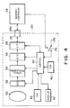
- Fig. 4 is a block diagram showing an arrangement of electric circuits of this embodiment.
- the same reference numerals as in Figs. 2, 3A, and 3B denote the same parts.
- the camera main body 20 includes a photographic lens 50, a CCD image pickup device 52, a signal processor 54, an A/D converter 56, an interface circuit 58 with respect to the memory cartridge 38, a controller 60 constituted by a microcomputer for controlling the overall system, and a switch 62 for inputting various commands.
- the image pickup device 52 converts an optical image of an object photographed by the photographic lens 50 into an electrical signal, and the signal processor 54 performs predetermined image signal processing.
- the A/D converter 56 digitizes an output from the signal processor 54. An output from the A/D converter 56 is supplied to and stored in the memory cartridge 38 via the interface circuit 58 and the contacts 28 and 38a.
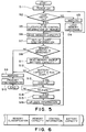
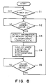
- Fig. 5 shows a control operation flow chart for performing checking in the above solid-state camera.
- the controller 60 checks an open/close state of the loading detection switch 26 (S2). If an unloaded state is detected, the controller 60 performs warning by the display device 32 and/or a sound so as to cause the user to load the memory cartridge 38 (S4). If the memory cartridge 38 is already loaded, the controller 60 reads out various pieces of specification information stored beforehand in the loaded memory cartridge 38 (S5 and S6) and displays the readout information on the display device 32 (S7).
- Fig. 6 shows the format of communication data from the memory circuit 38 to the camera main body 20.
- the controller 60 displays on the display device 32 (S9) a warning indicating that photographing cannot be performed, and prohibits photography (S10). If, however, sufficient memory capacity is left, the controller 60 reads the backup battery capacity of the memory cartridge 38 (S11) remaining. If the battery capacity is below a predetermined value, the controller 60 displays that photographing cannot be performed on the display device 32 and prohibits photographing (S9 and S10). If the battery capacity is over the predetermined value, the controller 60 displays that photographing can be performed (S13), waits for release (S14), and performs photographing/recording (i.e., writes an output from the image pickup device 52 in the memory cartridge 38) (S15). After recording (S15), the controller 60 updates information concerning the number of photographed frames, the remaining memory capacity, and the like (S16). The flow then returns to step S6, and the controller 60 checks the memory capacity and the backup battery capacity and waits for the next release.
- the flow may be modified such that a communication with the memory cartridge 38 is directly performed without checking the open/close state of the loading detection switch 26 immediately after the power source is switched on, and if the communication cannot be performed, non-loading or defective loading of the memory cartridge is warned to prohibit photographing.
- the switch 26 is separately provided to detect loading completion of the memory cartridge 38.
- Some of the electric contacts 28 of the camera main body 20, however, may be used to detect loading. In this case, two contacts 28a of a plurality of electric contacts 28 are used for loading detection, and remaining contacts 28b are used for communication. One of the contacts 28 for loading detection is to be grounded.
- the memory contacts 38a are electrically connected to the contacts 28. In accordance with whether an electrical signal (voltage value or current value) from the contact 28a is lower or higher than a predetermined level, the controller 60 of the camera main body 20 checks whether loading is completed.
- all the electric contacts 28 can be used for both loading detection and communication in such a manner that loading detection and data communication are performed at different timings. In this manner, the number of contacts 28 and 38a can be reduced.
- a solid-state camera according to another embodiment of the present invention will be described below with reference to Figs. 7 to 9.
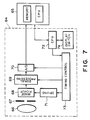
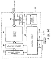
- Fig. 7 is a block diagram showing an arrangement of the embodiment in which the present invention is applied to a solid-state camera using a solid-state memory apparatus similar to the memory cartridge 38 of the above embodiment as a still image recording medium.
- a solid-state memory apparatus 65 comprising various IC memory devices and a CPU as a controller for controlling the IC memory devices can be detached from a camera main body 64.
- the solid-state memory apparatus 65 exchanges various information with the camera main body 64 via a predetermined bus line.
- the camera main body 64 comprises a photographic lens 66, a shutter 67, a solid-state image pickup device 68 such as a CCD, a signal processor 69, an A/D converter 70, a driver 71 for the image pickup device 68, a CPU 72 for controlling the overall system, a timing controller 73 for defining operation timings of the processor 69, the converter 70, and the driver 71 of the image pickup device 68, and a display/switch unit 74 including various switches and a display device.
- Fig. 7 An operation of Fig. 7 will be described below with reference to a flow chart shown in Fig. 8.
- S1 When a power switch of the camera main body 64 is turned on (S1), loading of the solid-state memory apparatus 65 is awaited (S2).
- the CPU 72 communicates with the loaded solid-state memory apparatus 65 and detects specification information (e.g., memory device classification, a transfer speed upper limit, and a remaining capacity shown in Fig. 6) of the solid-state memory apparatus 65 (S3). On the basis of this information, the CPU 72 determines operation speeds of the device 68, the processor 69, the converter 70, and the driver 71 and controls the timing controller 73.
- specification information e.g., memory device classification, a transfer speed upper limit, and a remaining capacity shown in Fig. 6
- the CPU 72 Since a maximum continuous photographing speed is determined on the basis of the memory information obtained in step S3, the CPU 72 displays a possible maximum continuous photographing speed (S4), and monitors unloading of the solid-state memory apparatus 65 (S5).
- Fig. 9 is a block diagram showing an arrangement of still another embodiment of the present invention.
- the same reference numerals as in Fig. 7 denote the same parts.
- image data digitized by an A/D converter 70 is temporarily stored in a frame memory 75.
- the image data temporarily stored in the frame memory 75 is read out from the frame memory 75 at a speed corresponding to a transfer speed of a memory device of a solid-state memory 75 and written in the solid-state memory apparatus 65.
- the above embodiment employs an arrangement in which when the solid-state memory 65 is loaded, the CPU 72 of the camera main body 64 inquires classification of a memory device used as the solid-state memory apparatus 65.
- the arrangement may be made such that the above various types of information are mechanically set in the solid-state memory apparatus 65 and detecting means for detecting the mechanically set information may be provided for the camera main body 64. With this arrangement, the CPU need not communicate with the memory.
- the maximum continuous photographing speed of the solid-state camera is limited to a write enable speed of the solid-state memory apparatus 65 and displayed. Therefore, operability of the solid-state camera, especially its continuous photographing operability is improved.
- the solid-state camera has been exemplified.
- the present invention can be generally applied to an apparatus for recording a certain kind of information in a detachable solid-state memory apparatus.
- solid-state memory apparatus is obtained by applying the present invention to the memory cartridge and the solid-state memory apparatus of the above embodiments.
- Fig. 10 is a block diagram showing an arrangement of the embodiment of the present invention.
- a solid-state memory apparatus 65 includes a status output line 76, an address/control input line 77, a clock input line 78, and a data input/output line 79.
- the data input/output line 79 is constituted by one signal line.
- the data input/output line is constituted by signal lines in the number corresponding to the number of parallel signals.
- the solid-state memory apparatus 65 also includes a memory device 80, an address counter 81, an address preset circuit 82, a controller 83, a recognition code storing circuit 84, and a buffer 85.
- the input lines 77 and 78 and the input/output line 79 are connected to a solid-state camera via electric contacts as shown in Fig. 3.
- an operation mode of the solid-state memory apparatus 65 is set. That is, a clock signal is supplied to the clock input line 78 and a binary signal is supplied to the address/control input line 77 at timings shown in Fig. 11.
- the controller 83 decodes a command from the address/control input line 77 and operates the respective sections by the designated operation mode.
- image data can be randomly accessed by designating the number of a photograph. That is, when the number of photographs to be read is designated, the address preset circuit 82 loads its start address in the address counter 81, and the address counter 81 sequentially counts up. In this manner, write or read of a storage area corresponding to the designated number can be performed.
- a recognition code can be output from the recognition code storing circuit 84 to the camera main body. More specifically, when "0111" is supplied from the camera main body to the address/control input line 77, the controller 83 sends a command to the recognition code storing circuit 84 to output a stored recognition code. This recognition code is output to the camera main body via the output buffer 85 and the data input/output line 79. Note that the recognition code storing circuit 84 stores various types of specification information as shown in Fig. 6.
- Fig. 12 is a timing chart for explaining the above operation.
- a clock signal is normally supplied from the camera main body to the solid-state memory apparatus 65, and the internal circuit in the solid-state memory apparatus 65 operates in synchronism with this clock.
- a readout command "0111" of memory recognition code is supplied from the camera main body to the address/control input line 77 at the timing shown in Fig. 12. The first “0" is a start bit.
- the controller 83 interprets this command and sets a status bit at "H", thereby informing the camera main body that the data is effective.
- the controller 83 causes the recognition code storing circuit 84 to output storage data (in this embodiment, "00101100") to the data input/output line 79 via the buffer 85.
- a read-only memory or a combinational logic circuit, e.g., is used as the recognition code storing circuit 84.
- this recognition code may be determined to include information such as a memory capacity, a transfer rate, and an image size, its length is not limited to 8 bits.
- the recognition code is read out by a command response scheme.
- An exclusive readout terminal may be used to read out the code.
- data exchange is performed by four types of signal lines. Data exchange, however, may be performed by using a larger or smaller number of signal lines.
- a new electronic device can be used to achieve a large capacity and a high speed.
Landscapes
- Engineering & Computer Science (AREA)
- Multimedia (AREA)
- Signal Processing (AREA)
- Television Signal Processing For Recording (AREA)
- Studio Devices (AREA)
Claims (15)
- Appareil photographique à semiconducteurs (10) destiné à être utilisé avec des moyens amovibles (12, 38, 65) de stockage d'image à semiconducteurs ledit appareil photographique comportant:
des moyens de détection (28, 58, 60, 72), pouvant coopérer avec lesdits moyens (38, 65) de stockage d'image à semiconducteurs pour détecter à partir d'indications fournies par lesdits moyens (38, 65) de stockage d'image à semiconducteurs un ou plusieurs des paramètres suivants:(a) une capacité de stockage de mémoire restante desdits moyens (38, 65) de stockage d'images à semiconducteurs à l'instant du chargement desdits moyens de stockage d'images à semiconducteurs amovibles et directement après chaque exposition;(b) une capacité de puissance restante d'une source d'alimentation de réserve (-) incorporée dans lesdits moyens (38, 65) de stockage d'images à semiconducteurs; et(c) une vitesse d'écriture maximum pour l'enregistrement dans une mémoire de stockage desdits moyens (38, 65) de stockage d'images à semiconducteurs de données d'images produites par ledit appareil photographique; etdes moyens (60, 72) de commande du fonctionnement de l'appareil photographique sensibles auxdits moyens de détection (28, 58, 60, 72) pour commander le fonctionnement dudit appareil photographique, afin d'effectuer les opérations suivantes:(i) empêcher le fonctionnement et avertir avant de libérer l'exposition dans l'éventualité où il est détecté soit qu'il n'y a plus de capacité de stockage de mémoire restante, soit que la capacité de puissance restante est inférieure à un niveau prédéterminé; et/ou(ii) commander une cadence de transfert de données d'images à partir dudit appareil photographique (10) vers lesdits moyens (38, 65) de stockage d'images à semiconducteurs en fonction de la vitesse d'écriture maximum indiquée par lesdits moyens (38, 65) de stockage d'images à semiconducteurs et détectée par lesdits moyens de détection (28, 58, 60, 72); et/ou(iii) commander une vitesse de photographie en continu en fonction de ladite vitesse d'écriture maximum qui est à la fois indiquée par lesdits moyens (38, 65) de stockage d'images à semiconducteurs et détectée par lesdits moyens de détection (28, 58, 60, 72). - Appareil photographique selon la revendication 1, dans lequel:
lesdits moyens de détection (28, 58, 60, 72) peuvent fonctionner pour détecter tous lesdits paramètres respectifs (a) à (c); et
lesdits moyens (60, 72) de commande du fonctionnement de l'appareil photographique peuvent fonctionner pour effectuer toutes lesdites opérations (i) à (iii). - Appareil photographique selon l'une quelconque des revendications 1 et 2, dans lequel lesdits moyens de détection (28, 58, 60, 72) et lesdits moyens (60, 72) de commande du fonctionnement de l'appareil photographique comportent un microcalculateur (60, 72).
- Appareil photographique selon l'une quelconque des revendications précédentes, dans lequel lesdits moyens de détection (28, 58, 60, 72) comportent:
des moyens d'accès (60, 72) pour accéder aux données de spécification stockées dans lesdits moyens (38, 65) de stockage d'images à semiconducteurs; et
des moyens d'interface (28, 58) pour recevoir lesdites données de spécification;
ces données de spécification fournissant lesdites indications de l'un ou plusieurs des paramètres respectifs (a) à (c). - Appareil photographique selon la revendication 4, dans lequel lesdits moyens d'accès (60) peuvent fonctionner pour lire lesdites données de spécification stockées dans ledit moyen (38) de stockage d'images à semiconducteurs.
- Appareil photographique selon la revendication 5, dans lequel lesdits moyens d'accès (60) peuvent fonctionner pour lire de manière séquentielle des données de spécification indicatrices des paramètres (a) et (b) respectivement.
- Appareil photographique selon la revendication 6, comprenant des moyens de mise à jour (60) ces moyens de mise à jour pouvant coopérer avec lesdits moyens (38) de stockage d'image à semiconducteurs pour mettre à jour lesdits paramètres respectifs (a) et (b) suivant le fonctionnement desdits moyens d'accès (60) et suivant un enregistrement de données d'images dans lesdits moyens (38) de stockage d'images à semiconducteurs.
- Appareil photographique selon l'une quelconque des revendications précédentes, dans lequel lesdits moyens de détection (28, 58, 60) peuvent coopérer avec lesdits moyens (38) de stockage d'images à semiconducteurs pour détecter au moins l'un desdits paramètres respectifs (a) ou (b), ledit appareil photographique ayant un panneau d'affichage (32), et lesdits moyens (60) de commande du fonctionnement de l'appareil photographique pouvant coopérer avec ledit panneau d'affichage (32) pour amener ledit panneau d'affichage (32) à afficher une indication d'avertissement dans l'éventualité où il est détecté par lesdits moyens de détection (28, 58, 60) soit qu'il n'y a pas de capacité de mémoire restante, soit que la capacité de puissance restante est inférieure audit niveau prédéterminé, respectivement.
- Appareil photographique selon l'une quelconque des revendications précédentes, dans lequel lesdits moyens de détection (28, 58, 60) comportent des moyens, pouvant coopérer avec lesdits moyens (12, 38, 65) de stockage d'images à semiconducteurs amovibles, pour détecter une information de classification établie mécaniquement dans lesdits moyens (38, 65) de stockage d'images à semiconducteurs et comportant ladite vitesse d'écriture maximum.
- Appareil photographique selon l'une quelconque des revendications précédentes et comportant un moyen (75) formant tampon de mémoire de trame pour stocker des données d'images produites par ledit appareil photographique avant le transfert vers ledit moyen (65) d'image à semiconducteurs.
- Appareil photographique selon l'une quelconque des revendications précédentes, comportant un moyen (26) de détection de chargement pour détecter un chargement complet desdits moyens de stockage d'images à semiconducteurs amovibles, et des moyens d'avertissement (32) sensibles auxdits moyens de détection de chargement (26) pour avertir dans l'éventualité où ce chargement est incomplet.
- Appareil photographique selon la revendication 11, dans lequel lesdits moyens (26) de détection de chargement comportent un commutateur (26) de détection de chargement.
- Moyen (65) de stockage d'images à semiconducteurs amovible destiné à être utilisé avec un appareil photographique selon la revendication 1, et pouvant être fixé à celui-ci, ce moyen (65) de stockage d'images comportant:
un stockage (80) à mémoire de données d'images pour stocker des données d'images; et
des moyens d'information (79, 84, 85) pour stocker l'un quelconque ou plusieurs des paramètres respectifs (a) à (c) cités dans la revendication 1, ces moyens d'information (79, 83, 84, 85) pouvant coopérer avec ledit appareil photographique à semiconducteurs et étant effectifs pour transférer l'indication desdits un ou plusieurs paramètres en provenance dudit moyen (65) de stockage d'images vers ledit appareil photographique à semiconducteurs, afin de commander le réglage automatique et le fonctionnement de celui-ci. - Moyen de stockage d'images selon la revendication 13, dans lequel lesdits moyens d'information (79, 84, 85) comportent une mémoire (84) de code de reconnaissance contenant des données d'indication transférables pour un quelconque ou plusieurs des paramètres respectifs (a) à (c).
- Appareil photographique chargé comprenant la combinaison pouvant coopérer d'un appareil photographique à semiconducteurs selon la revendication 1 et d'un moyen (65) de stockage d'images à semiconducteurs amovible selon l'une quelconque des revendications 13 ou 14.
Applications Claiming Priority (6)
| Application Number | Priority Date | Filing Date | Title |
|---|---|---|---|
| JP63269558A JPH02118990A (ja) | 1988-10-27 | 1988-10-27 | 固体メモリ装置 |
| JP269558/88 | 1988-10-27 | ||
| JP1039343A JP2712489B2 (ja) | 1989-02-21 | 1989-02-21 | 固体カメラ |
| JP39343/89 | 1989-02-21 | ||
| JP1079587A JPH02257341A (ja) | 1989-03-30 | 1989-03-30 | 情報記録装置 |
| JP79587/89 | 1989-03-30 |
Publications (2)
| Publication Number | Publication Date |
|---|---|
| EP0366474A1 EP0366474A1 (fr) | 1990-05-02 |
| EP0366474B1 true EP0366474B1 (fr) | 1994-12-28 |
Family
ID=27290108
Family Applications (1)
| Application Number | Title | Priority Date | Filing Date |
|---|---|---|---|
| EP89311078A Expired - Lifetime EP0366474B1 (fr) | 1988-10-27 | 1989-10-26 | Caméra à semi-conducteurs et appareil de mémoire à semi-conducteurs |
Country Status (3)
| Country | Link |
|---|---|
| US (1) | US6118929A (fr) |
| EP (1) | EP0366474B1 (fr) |
| DE (1) | DE68920273T2 (fr) |
Families Citing this family (27)
| Publication number | Priority date | Publication date | Assignee | Title |
|---|---|---|---|---|
| JPH04241335A (ja) * | 1991-01-14 | 1992-08-28 | Fuji Photo Film Co Ltd | メモリ・カード内蔵電池電圧低下警告機能付ディジタル電子スチル・カメラ |
| EP0772358A1 (fr) * | 1991-08-09 | 1997-05-07 | Kabushiki Kaisha Toshiba | Appareil d'enregistrement sur une carte à mémoire |
| JP3397345B2 (ja) * | 1992-08-31 | 2003-04-14 | キヤノン株式会社 | 記録媒体のローディング機構 |
| GB9607770D0 (en) * | 1996-04-15 | 1996-06-19 | Euroquest Solutions Ltd | Imaging system |
| NZ299938A (en) | 1996-12-13 | 1999-02-25 | Disposable Video Camcorders Lt | Disposable video recorder comprises lens, light sensing means, signal processing means, recording medium mounting means, write means, casing and means for limiting the useful life of a component |
| US6587140B2 (en) * | 1997-10-23 | 2003-07-01 | Eastman Kodak Company | System and method for using a single intelligence circuit in both a digital camera and printer |
| US6738090B2 (en) | 1997-10-23 | 2004-05-18 | Eastman Kodak Company | System and method for using a single intelligence circuit for a plurality of imaging rendering components |
| JPH11331764A (ja) * | 1998-03-20 | 1999-11-30 | Sony Corp | 記録再生装置及び方法 |
| JP2002209132A (ja) * | 2001-01-12 | 2002-07-26 | Minolta Co Ltd | デジタルカメラ |
| US6930727B2 (en) * | 2001-03-30 | 2005-08-16 | Sony Corporation | Protection-cover opening/closing mechanism for recording/playback apparatus |
| US7765334B2 (en) * | 2004-05-12 | 2010-07-27 | Canon Kabushiki Kaisha | Electronic apparatus for use with removable storage medium, control method therefor, and program for implementing the method |
| US20070076325A1 (en) * | 2005-09-20 | 2007-04-05 | Nokia Corporation | Apparatus for indicating a state of a device |
| KR101467928B1 (ko) * | 2007-07-23 | 2014-12-04 | 삼성전자주식회사 | 기기정보를 출력하는 a/v기기 및 그 기기정보출력방법 |
| WO2010005975A1 (fr) | 2008-07-07 | 2010-01-14 | Woodman Labs | Boîtier d’appareil photo avec module d’extension intégré |
| USD890835S1 (en) | 2017-12-28 | 2020-07-21 | Gopro, Inc. | Camera |
| WO2020033389A1 (fr) | 2018-08-07 | 2020-02-13 | Gopro, Inc. | Caméra et support de caméra |
| USD905786S1 (en) | 2018-08-31 | 2020-12-22 | Gopro, Inc. | Camera mount |
| USD894256S1 (en) | 2018-08-31 | 2020-08-25 | Gopro, Inc. | Camera mount |
| USD920419S1 (en) | 2019-09-17 | 2021-05-25 | Gopro, Inc. | Camera |
| USD946074S1 (en) | 2020-08-14 | 2022-03-15 | Gopro, Inc. | Camera |
| USD1107775S1 (en) | 2022-08-04 | 2025-12-30 | Gopro, Inc. | Camera |
| US12321084B2 (en) | 2022-08-12 | 2025-06-03 | Gopro, Inc. | Interconnect mechanism for image capture device |
| US12379650B2 (en) | 2023-02-15 | 2025-08-05 | Gopro, Inc. | Reinforced image capture devices including interconnect mechanisms with a threaded accessory interface |
| US12574622B2 (en) | 2024-03-15 | 2026-03-10 | Gopro, Inc. | Image capture apparatus including a multi-function interconnect mechanism |
| USD1096914S1 (en) | 2024-03-15 | 2025-10-07 | Gopro, Inc. | Camera mount |
| USD1100025S1 (en) | 2024-03-15 | 2025-10-28 | Gopro, Inc. | Camera mount |
| USD1118735S1 (en) | 2024-05-22 | 2026-03-17 | Gopro, Inc. | Camera |
Family Cites Families (23)
| Publication number | Priority date | Publication date | Assignee | Title |
|---|---|---|---|---|
| JPS564992A (en) * | 1979-06-26 | 1981-01-19 | Olympus Optical Co Ltd | Recording and reproducing device |
| JPS5792981A (en) * | 1980-11-29 | 1982-06-09 | Nippon Kogaku Kk <Nikon> | Electronic camera system |
| JPS5714261A (en) * | 1980-06-30 | 1982-01-25 | Nippon Kogaku Kk <Nikon> | Charge storage time controller for solidstate image sensor |
| US4420773A (en) * | 1980-06-30 | 1983-12-13 | Nippon Kogaku K.K. | Electronic photographic camera |
| BE890517A (fr) * | 1981-09-28 | 1982-01-18 | Staar Sa | Dispositif de memorisation d'images electroniques |
| JPS58155586A (ja) * | 1982-03-10 | 1983-09-16 | Olympus Optical Co Ltd | 電子写真装置用デイスクパツク |
| US4651227A (en) * | 1982-08-20 | 1987-03-17 | Olympus Optical Co., Ltd. | Video signal recording apparatus with A/D conversion |
| JPS6230484A (ja) * | 1985-08-01 | 1987-02-09 | Nippon Kogaku Kk <Nikon> | 電子スチルカメラ |
| JPS62254249A (ja) * | 1986-04-28 | 1987-11-06 | Toshiba Corp | カード記憶容量読取り方式 |
| JP2538564B2 (ja) * | 1986-05-21 | 1996-09-25 | キヤノン株式会社 | 記録装置 |
| US4837628A (en) * | 1986-07-14 | 1989-06-06 | Kabushiki Kaisha Toshiba | Electronic still camera for recording still picture on memory card with mode selecting shutter release |
| JPH0654596B2 (ja) * | 1986-08-08 | 1994-07-20 | キヤノン株式会社 | 電子カメラ |
| JPS63100696A (ja) * | 1986-10-16 | 1988-05-02 | Fujitsu Ltd | 磁気バブルメモリカセツト装置 |
| KR910006609B1 (ko) * | 1986-12-18 | 1991-08-29 | 가시오 게이상기 가부시기가이샤 | 전자 스틸 카메라 |
| JPS63161787A (ja) * | 1986-12-24 | 1988-07-05 | Kyocera Corp | 電子スチ−ルカメラ |
| JPS63163588A (ja) * | 1986-12-25 | 1988-07-07 | Toshiba Corp | Icカ−ド |
| JPS63241761A (ja) * | 1987-03-30 | 1988-10-07 | Hitachi Ltd | 静止画記録再生装置 |
| US4907231A (en) * | 1987-05-06 | 1990-03-06 | Fuji Photo Film Co., Ltd. | Memory cartridge-connectable electronic device such as electronic still video camera |
| JPS63284988A (ja) * | 1987-05-18 | 1988-11-22 | Toshiba Corp | ディジタル電子カメラ |
| JPH0620283B2 (ja) * | 1987-05-19 | 1994-03-16 | 富士写真フイルム株式会社 | 画像デ−タ記録装置 |
| US4887161A (en) * | 1987-05-28 | 1989-12-12 | Fuji Photo Film Co., Ltd. | Memory cartridge and digital electronic still video camera in which said memory cartridge is freely loadable/unloadable |
| US4827347A (en) * | 1988-08-22 | 1989-05-02 | Eastman Kodak Company | Electronic camera with proofing feature |
| JP2712497B2 (ja) * | 1989-03-02 | 1998-02-10 | キヤノン株式会社 | 固体カメラ |
-
1989
- 1989-10-26 EP EP89311078A patent/EP0366474B1/fr not_active Expired - Lifetime
- 1989-10-26 DE DE68920273T patent/DE68920273T2/de not_active Expired - Fee Related
-
1995
- 1995-04-27 US US08/430,157 patent/US6118929A/en not_active Expired - Lifetime
Also Published As
| Publication number | Publication date |
|---|---|
| DE68920273D1 (de) | 1995-02-09 |
| EP0366474A1 (fr) | 1990-05-02 |
| US6118929A (en) | 2000-09-12 |
| DE68920273T2 (de) | 1995-05-11 |
Similar Documents
| Publication | Publication Date | Title |
|---|---|---|
| EP0366474B1 (fr) | Caméra à semi-conducteurs et appareil de mémoire à semi-conducteurs | |
| US5627587A (en) | Solid-state camera in which a removable solid state memory having a backup battery is used as an image recording device | |
| US6457647B1 (en) | Memory card adaptor to facilitate upgrades and the like | |
| GB2110042A (en) | Electronic still camera with individual non-volatile memory units | |
| US5159458A (en) | Camera sensing when a memory cartridge is installed | |
| US5821996A (en) | Solid-sate camera with solid-state memory for holding characteristic code representing characteristic of an internal circuit | |
| US5854875A (en) | Information recording appartus connectable to plural types of information recording media for recording information | |
| JPH053073B2 (fr) | ||
| US5822145A (en) | Information recording and/or reproducing apparatus using an information recording device having two kinds of recording media | |
| JPS63284987A (ja) | 電子スチルカメラ | |
| JP4058259B2 (ja) | 記憶媒体アクセス装置及び記憶媒体アクセス制御方法 | |
| JP4073225B2 (ja) | 電子アルバム装置 | |
| JP4408497B2 (ja) | 記録装置 | |
| JP4010784B2 (ja) | 複数メディアを対象とするデータ処理装置 | |
| JPH1188818A (ja) | 電子的撮像装置 | |
| JPH10145717A (ja) | 電子カメラ | |
| JPH02219376A (ja) | 固体カメラ | |
| JP2871720B2 (ja) | 情報記録装置 | |
| JP3458392B2 (ja) | スチルカメラ | |
| JP2759660B2 (ja) | 固体カメラ | |
| JP2767257B2 (ja) | 固体カメラ | |
| JP3143517B2 (ja) | 記録装置 | |
| JP2004118661A (ja) | Icメモリカートリッジ及び画像データ処理システム | |
| JPH02257341A (ja) | 情報記録装置 | |
| JP3140607B2 (ja) | 情報読み取り装置 |
Legal Events
| Date | Code | Title | Description |
|---|---|---|---|
| PUAI | Public reference made under article 153(3) epc to a published international application that has entered the european phase |
Free format text: ORIGINAL CODE: 0009012 |
|
| AK | Designated contracting states |
Kind code of ref document: A1 Designated state(s): DE FR GB |
|
| 17P | Request for examination filed |
Effective date: 19900918 |
|
| 17Q | First examination report despatched |
Effective date: 19920811 |
|
| GRAA | (expected) grant |
Free format text: ORIGINAL CODE: 0009210 |
|
| AK | Designated contracting states |
Kind code of ref document: B1 Designated state(s): DE FR GB |
|
| REF | Corresponds to: |
Ref document number: 68920273 Country of ref document: DE Date of ref document: 19950209 |
|
| ET | Fr: translation filed | ||
| PLBE | No opposition filed within time limit |
Free format text: ORIGINAL CODE: 0009261 |
|
| STAA | Information on the status of an ep patent application or granted ep patent |
Free format text: STATUS: NO OPPOSITION FILED WITHIN TIME LIMIT |
|
| 26N | No opposition filed | ||
| REG | Reference to a national code |
Ref country code: GB Ref legal event code: IF02 |
|
| PGFP | Annual fee paid to national office [announced via postgrant information from national office to epo] |
Ref country code: DE Payment date: 20071031 Year of fee payment: 19 |
|
| PGFP | Annual fee paid to national office [announced via postgrant information from national office to epo] |
Ref country code: FR Payment date: 20071022 Year of fee payment: 19 Ref country code: GB Payment date: 20071005 Year of fee payment: 19 |
|
| GBPC | Gb: european patent ceased through non-payment of renewal fee |
Effective date: 20081026 |
|
| REG | Reference to a national code |
Ref country code: FR Ref legal event code: ST Effective date: 20090630 |
|
| PG25 | Lapsed in a contracting state [announced via postgrant information from national office to epo] |
Ref country code: DE Free format text: LAPSE BECAUSE OF NON-PAYMENT OF DUE FEES Effective date: 20090501 |
|
| PG25 | Lapsed in a contracting state [announced via postgrant information from national office to epo] |
Ref country code: FR Free format text: LAPSE BECAUSE OF NON-PAYMENT OF DUE FEES Effective date: 20081031 |
|
| PG25 | Lapsed in a contracting state [announced via postgrant information from national office to epo] |
Ref country code: GB Free format text: LAPSE BECAUSE OF NON-PAYMENT OF DUE FEES Effective date: 20081026 |