EP0366517A1 - Paralleler Analog-Digitalwandler mit Fehlerkorrekturschaltung - Google Patents
Paralleler Analog-Digitalwandler mit Fehlerkorrekturschaltung Download PDFInfo
- Publication number
- EP0366517A1 EP0366517A1 EP89402785A EP89402785A EP0366517A1 EP 0366517 A1 EP0366517 A1 EP 0366517A1 EP 89402785 A EP89402785 A EP 89402785A EP 89402785 A EP89402785 A EP 89402785A EP 0366517 A1 EP0366517 A1 EP 0366517A1
- Authority
- EP
- European Patent Office
- Prior art keywords
- comparator
- stage
- corr
- output
- comparators
- Prior art date
- Legal status (The legal status is an assumption and is not a legal conclusion. Google has not performed a legal analysis and makes no representation as to the accuracy of the status listed.)
- Granted
Links
- 238000010586 diagram Methods 0.000 description 13
- 239000012634 fragment Substances 0.000 description 3
- 230000007704 transition Effects 0.000 description 3
- 229910001218 Gallium arsenide Inorganic materials 0.000 description 1
- 238000006243 chemical reaction Methods 0.000 description 1
- 238000009434 installation Methods 0.000 description 1
- 239000000463 material Substances 0.000 description 1
- 238000005259 measurement Methods 0.000 description 1
- 229910052710 silicon Inorganic materials 0.000 description 1
- 239000010703 silicon Substances 0.000 description 1
Images
Classifications
-
- H—ELECTRICITY
- H03—ELECTRONIC CIRCUITRY
- H03M—CODING; DECODING; CODE CONVERSION IN GENERAL
- H03M1/00—Analogue/digital conversion; Digital/analogue conversion
- H03M1/06—Continuously compensating for, or preventing, undesired influence of physical parameters
- H03M1/08—Continuously compensating for, or preventing, undesired influence of physical parameters of noise
- H03M1/0809—Continuously compensating for, or preventing, undesired influence of physical parameters of noise of bubble errors, i.e. irregularities in thermometer codes
-
- H—ELECTRICITY
- H03—ELECTRONIC CIRCUITRY
- H03M—CODING; DECODING; CODE CONVERSION IN GENERAL
- H03M1/00—Analogue/digital conversion; Digital/analogue conversion
- H03M1/12—Analogue/digital converters
- H03M1/34—Analogue value compared with reference values
- H03M1/36—Analogue value compared with reference values simultaneously only, i.e. parallel type
Definitions
- the present invention relates to an improvement to parallel analog-digital converters, called “flash": this improvement consists in introducing a logic correction stage placed between the stage of the comparators and the stage of the encoder. This correction stage forces the output of a comparator, which is accidentally erroneous, to take the same logic value, 0 or 1, as the outputs of the two neighboring comparators if these are identical.
- the correction circuit according to the invention forces O logic to output a comparator which supplies a logic 1, while the two comparators which frame it both provide a logic 0. And conversely, it forces a logic 1 to output a comparator that provides a logic 0 if the two comparators that surround it provide a logic 1.
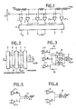
- an analog-to-digital converter of the "flash" type - there are other ADC structures - comprises, as very briefly recalled in FIG. 1, a first stage of comparators mounted in parallel and marked 1.2. .i, i + 1, ... 2 n -2, 2 n -1, if the ADC must supply a logic signal formed by n bits.
- the analog signal to be converted, at input E, is applied in parallel to all the first comparator inputs.
- Reference voltages, by equal discrete values, are taken from a voltage divider between V min and V max and applied to the second comparator inputs.
- the set of comparators and the voltage divider forms the comparator stage, marked 3, which provides what it is used to call a thermometric scale. This means that all the comparator outputs for which the analog voltage is higher than the reference voltage provide a logic signal 1. Conversely, all the comparator outputs for which the analog voltage is lower than the reference voltage provide a logic 0 signal.
- the invention therefore consists in introducing, in an analog-digital converter, a corrector stage between the comparator stage (CAN input) and the encoder stage (CAN output).
- This corrector stage forces the output of a comparator to take the same logic value as those of the two comparators which frame it if and only if said two logic values are identical, but opposite to that provided by the comparator considered, which is accidentally erroneous .
- the correcting circuit corrects this accident and provides a logic 1. Similarly, if a logic 1 is in the middle of a series of logic 0s, the correcting circuit corrects this accident and provides a logic 0.
- the correction circuit according to the invention is adapted to case of the two end comparators, which have only one neighbor: comparator 1 of the lightest bit, and comparator 2 n - 1 of the heaviest bit.
- the invention relates to a parallel analog-digital converter, called “flash”, comprising a first stage formed by a plurality of comparators (1 to 2 n -1) connected in parallel which transform an analog value applied to their common input into a binary value constituted by a series of 1 logics then of 0 logics, called thermometric scale, and also comprising a second encoder stage, which transforms the values of the thermometric scale into a binary number, this converter being characterized by what it further comprises, inserted between the first and second stages, a third stage, corrector, whose function is to correct the output value B of a comparator which is accidentally erroneous and has an anomaly in the scale thermometric, the corrector stage providing a corrected output value B corr . which is homogeneous with the thermometric scale.
- thermometric scale of a CAN flash which allows the encoder 4 to determine the binary number of conversion.
- thermometric scale which is accidentally tainted with an error on an output which will be called B: the corrector stage according to the invention provides at 7 a corrected thermometric scale, the value of which B corrected is correct.
- the corrector stage 5 is formed by a plurality of circuits, put in parallel, which will be suitable , to simplify writing, to call "cells".
- the correction cell corresponding to this output compares it to the output values of the two neighboring comparators, which frame it, as shown in Figure 3.
- the third column shows that there is forcing at logical 0, and the sixth column forcing at logical 1.
- each cell of the correction stage 5 comprises: - three AND doors 8.9 and 10, mounted in parallel, -one OR gate 11, in series with the three AND gates.
- the output B of comparator i is addressed to the first inputs (B) of the first and third AND gates 8 and 10.
- the output A of the comparator i + 1 is addressed to the second input (a) of the first AND gate 8 and to the first input (A) of the second AND gate 9.
- the output C of the comparator i-1 is addressed to the second input (C) of the third AND gate 10 and to the second input (C) of the second AND gate 9.
- the first AND gate 8 provides the Boolean function A.B (A and B) as an output
- the second gate 9 provides the A.C function (A and C)
- the third gate 10 provides the B.C function (B and C).
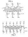
- the iterative diagram of the comparator stage 3 corresponds to an iterative diagram of the corrector stage 5, a fragment of which is represented in FIG. 4. This figure shows that the corrector stage is formed by a sub-stage of doors AND, in series with an understorey of OR doors.
- thermometric scale present a special case since they have only one neighbor.
- correction cells are shown in Figures 5 and 6.
- Figure 5 corresponds to the most significant comparator, of rank 2 n -1, or "from the top" of the thermometric scale. For this one, we are content to prohibit the logical 1, that is to say that we force it to logical 0, as soon as its neighbor of rank 2 n - 2 provides a logical 0. In the first Boolean function written above, it is [B and (A or C)] which represents forcing at logical 0. As A does not exist, all that is required is an AND gate 14 which provides BC
- Figure 7 gives the overall electrical diagram of the corrective stage of a CAN flash, including its two extreme cells, which are limited to: - an OR gate 15 for the lightest converter 1, - an AND gate 14 for the heaviest 2 n -1 converter.
- This corrector stage is applied to the realization of CAN flash, especially those which are integrated on fast materials of group III-V such as GaAs, but its diagram remains valid for slower CAN flash, on silicon, integrated circuit or discrete elements.
Landscapes
- Engineering & Computer Science (AREA)
- Theoretical Computer Science (AREA)
- Analogue/Digital Conversion (AREA)
Applications Claiming Priority (2)
| Application Number | Priority Date | Filing Date | Title |
|---|---|---|---|
| FR8813539A FR2638037B1 (fr) | 1988-10-14 | 1988-10-14 | Convertisseur analogique-numerique parallele, a circuit de correction d'erreur |
| FR8813539 | 1988-10-14 |
Publications (2)
| Publication Number | Publication Date |
|---|---|
| EP0366517A1 true EP0366517A1 (de) | 1990-05-02 |
| EP0366517B1 EP0366517B1 (de) | 1994-04-20 |
Family
ID=9371027
Family Applications (1)
| Application Number | Title | Priority Date | Filing Date |
|---|---|---|---|
| EP89402785A Expired - Lifetime EP0366517B1 (de) | 1988-10-14 | 1989-10-10 | Paralleler Analog-Digitalwandler mit Fehlerkorrekturschaltung |
Country Status (5)
| Country | Link |
|---|---|
| US (1) | US4983968A (de) |
| EP (1) | EP0366517B1 (de) |
| JP (1) | JPH02211719A (de) |
| DE (1) | DE68914777T2 (de) |
| FR (1) | FR2638037B1 (de) |
Cited By (1)
| Publication number | Priority date | Publication date | Assignee | Title |
|---|---|---|---|---|
| EP0792023A3 (de) * | 1995-08-14 | 1999-12-08 | Nec Corporation | Hochgeschwindigkeits- und Hochgenauigkeits-Analog-Digital-Wandler |
Families Citing this family (6)
| Publication number | Priority date | Publication date | Assignee | Title |
|---|---|---|---|---|
| US5237326A (en) * | 1989-02-02 | 1993-08-17 | Samsung Electronics Co., Ltd. | Flash type analog-to-digital converter having MOS comparators |
| US5781132A (en) * | 1996-01-17 | 1998-07-14 | Brooktree Corporation | Error correcting decoder |
| US6034631A (en) * | 1998-02-04 | 2000-03-07 | Lucent Technologies Inc. | Comparator error correction in flash analog-to-digital converter |
| JP3339566B2 (ja) * | 1998-10-21 | 2002-10-28 | 日本電気株式会社 | サーモメトリック−バイナリコード変換方法および回路、それに使用されるエンコーダ素子回路 |
| DE10060159A1 (de) * | 2000-12-04 | 2002-06-13 | Infineon Technologies Ag | Analog-Digital-Wandler und Verfahren zur Wandlung eines Analogsignals in ein Digitalsignal |
| GB2486455A (en) * | 2010-12-15 | 2012-06-20 | St Microelectronics Res & Dev | Error correction in thermometer codes |
Citations (2)
| Publication number | Priority date | Publication date | Assignee | Title |
|---|---|---|---|---|
| US4586025A (en) * | 1985-10-04 | 1986-04-29 | Tektronix, Inc. | Error tolerant thermometer-to-binary encoder |
| US4712087A (en) * | 1987-02-09 | 1987-12-08 | Tektronix, Inc. | Analog-to-digital converter error correction circuit |
Family Cites Families (6)
| Publication number | Priority date | Publication date | Assignee | Title |
|---|---|---|---|---|
| US3537101A (en) * | 1967-01-04 | 1970-10-27 | Us Army | High speed analog-to-digital encoder |
| US3611350A (en) * | 1970-02-12 | 1971-10-05 | Us Navy | High-speed parallel analog-to-digital converter |
| JPS5871726A (ja) * | 1981-10-26 | 1983-04-28 | Nec Corp | アナログ−デジタル変換器 |
| JPS59171315A (ja) * | 1983-03-18 | 1984-09-27 | Nec Corp | アナログ−デジタル変換器 |
| US4884075A (en) * | 1988-05-19 | 1989-11-28 | Analog Devices, Inc. | Decoding circuit for flash-type analog-to-digital converter |
| US4897657A (en) * | 1988-06-13 | 1990-01-30 | Integrated Device Technology, Inc. | Analog-to-digital converter having error detection and correction |
-
1988
- 1988-10-14 FR FR8813539A patent/FR2638037B1/fr not_active Expired - Fee Related
-
1989
- 1989-10-10 US US07/418,538 patent/US4983968A/en not_active Expired - Fee Related
- 1989-10-10 DE DE68914777T patent/DE68914777T2/de not_active Expired - Fee Related
- 1989-10-10 EP EP89402785A patent/EP0366517B1/de not_active Expired - Lifetime
- 1989-10-16 JP JP1268859A patent/JPH02211719A/ja active Pending
Patent Citations (2)
| Publication number | Priority date | Publication date | Assignee | Title |
|---|---|---|---|---|
| US4586025A (en) * | 1985-10-04 | 1986-04-29 | Tektronix, Inc. | Error tolerant thermometer-to-binary encoder |
| US4712087A (en) * | 1987-02-09 | 1987-12-08 | Tektronix, Inc. | Analog-to-digital converter error correction circuit |
Cited By (1)
| Publication number | Priority date | Publication date | Assignee | Title |
|---|---|---|---|---|
| EP0792023A3 (de) * | 1995-08-14 | 1999-12-08 | Nec Corporation | Hochgeschwindigkeits- und Hochgenauigkeits-Analog-Digital-Wandler |
Also Published As
| Publication number | Publication date |
|---|---|
| US4983968A (en) | 1991-01-08 |
| DE68914777D1 (de) | 1994-05-26 |
| FR2638037B1 (fr) | 1994-04-08 |
| DE68914777T2 (de) | 1994-08-11 |
| FR2638037A1 (fr) | 1990-04-20 |
| JPH02211719A (ja) | 1990-08-23 |
| EP0366517B1 (de) | 1994-04-20 |
Similar Documents
| Publication | Publication Date | Title |
|---|---|---|
| US7256725B2 (en) | Resistor ladder interpolation for subranging ADC | |
| KR970005828B1 (ko) | 파이프 라인 구조의 다단 아날로그/디지탈 변환기 | |
| EP1131888B1 (de) | Verfahren zum kalibrieren eines analog-digital wandlers und eine kalibrierungsvorrichtung | |
| KR0179466B1 (ko) | 디지탈-아날로그 변환기 및 이를 구비한 집적회로와 디지탈-아날로그 신호 변환 방법 | |
| US20140232582A1 (en) | Analog-to-digital converter for a multi-channel signal acquisition system | |
| US8094056B2 (en) | Analog-to-digital converter | |
| US20080088493A1 (en) | Resistor Ladder Interpolation for PGA and DAC | |
| US20090096647A1 (en) | Analog-to-digital converter | |
| US6426715B1 (en) | Digital to analog converter | |
| EP0760181B1 (de) | Automatische kalibrierungsschaltung mit einer referenzskala für einen digital-analogen wandler | |
| US5389929A (en) | Two-step subranging analog-to-digital converter | |
| US6222478B1 (en) | Pipeline analog-to-digital conversion system using a modified coding scheme and method of operation | |
| EP0366517B1 (de) | Paralleler Analog-Digitalwandler mit Fehlerkorrekturschaltung | |
| US6515611B1 (en) | Multistage analog-to-digital converter with amplifier component swapping for improved linearity | |
| US6784818B2 (en) | Analog to digital converter with interpolation of reference ladder | |
| US6304204B1 (en) | Error correction architecture for pipeline analog to digital converters | |
| US20060145908A1 (en) | Pipelined analog-to-digital converter having enhanced high frequency performance characteristics | |
| JP2995599B2 (ja) | アナログデジタル変換方法 | |
| US7221191B2 (en) | Signal samplers with enhanced dynamic range | |
| US6317070B1 (en) | Floating-point analog-to-digital converter | |
| EP1269635B1 (de) | Hintergrundkalibrierung eines a/d-umsetzers | |
| US20060187108A1 (en) | Reference voltage driving circuit and pipelined analog to digital converter including same | |
| Kolluri | A 12-bit 500-ns subranging ADC | |
| US7248199B2 (en) | Analog-to-digital converter | |
| US20080106446A1 (en) | Self-calibrating pipeline analog-to-digital converter and method of calibrating a pipeline analog-to-digital converter |
Legal Events
| Date | Code | Title | Description |
|---|---|---|---|
| PUAI | Public reference made under article 153(3) epc to a published international application that has entered the european phase |
Free format text: ORIGINAL CODE: 0009012 |
|
| AK | Designated contracting states |
Kind code of ref document: A1 Designated state(s): DE GB NL |
|
| 17P | Request for examination filed |
Effective date: 19900518 |
|
| 17Q | First examination report despatched |
Effective date: 19930831 |
|
| RAP1 | Party data changed (applicant data changed or rights of an application transferred) |
Owner name: THOMSON-CSF SEMICONDUCTEURS SPECIFIQUES |
|
| GRAA | (expected) grant |
Free format text: ORIGINAL CODE: 0009210 |
|
| AK | Designated contracting states |
Kind code of ref document: B1 Designated state(s): DE GB NL |
|
| REF | Corresponds to: |
Ref document number: 68914777 Country of ref document: DE Date of ref document: 19940526 |
|
| GBT | Gb: translation of ep patent filed (gb section 77(6)(a)/1977) |
Effective date: 19940609 |
|
| PLBE | No opposition filed within time limit |
Free format text: ORIGINAL CODE: 0009261 |
|
| STAA | Information on the status of an ep patent application or granted ep patent |
Free format text: STATUS: NO OPPOSITION FILED WITHIN TIME LIMIT |
|
| 26N | No opposition filed | ||
| PGFP | Annual fee paid to national office [announced via postgrant information from national office to epo] |
Ref country code: NL Payment date: 19950915 Year of fee payment: 7 |
|
| PGFP | Annual fee paid to national office [announced via postgrant information from national office to epo] |
Ref country code: GB Payment date: 19950920 Year of fee payment: 7 |
|
| PGFP | Annual fee paid to national office [announced via postgrant information from national office to epo] |
Ref country code: DE Payment date: 19950923 Year of fee payment: 7 |
|
| PG25 | Lapsed in a contracting state [announced via postgrant information from national office to epo] |
Ref country code: GB Effective date: 19961010 |
|
| PG25 | Lapsed in a contracting state [announced via postgrant information from national office to epo] |
Ref country code: NL Effective date: 19970501 |
|
| GBPC | Gb: european patent ceased through non-payment of renewal fee |
Effective date: 19961010 |
|
| NLV4 | Nl: lapsed or anulled due to non-payment of the annual fee |
Effective date: 19970501 |
|
| PG25 | Lapsed in a contracting state [announced via postgrant information from national office to epo] |
Ref country code: DE Effective date: 19970701 |