EP0366517B1 - Paralleler Analog-Digitalwandler mit Fehlerkorrekturschaltung - Google Patents
Paralleler Analog-Digitalwandler mit Fehlerkorrekturschaltung Download PDFInfo
- Publication number
- EP0366517B1 EP0366517B1 EP89402785A EP89402785A EP0366517B1 EP 0366517 B1 EP0366517 B1 EP 0366517B1 EP 89402785 A EP89402785 A EP 89402785A EP 89402785 A EP89402785 A EP 89402785A EP 0366517 B1 EP0366517 B1 EP 0366517B1
- Authority
- EP
- European Patent Office
- Prior art keywords
- comparator
- stage
- output
- corr
- gate
- Prior art date
- Legal status (The legal status is an assumption and is not a legal conclusion. Google has not performed a legal analysis and makes no representation as to the accuracy of the status listed.)
- Expired - Lifetime
Links
Images

Classifications
-
- H—ELECTRICITY
- H03—ELECTRONIC CIRCUITRY
- H03M—CODING; DECODING; CODE CONVERSION IN GENERAL
- H03M1/00—Analogue/digital conversion; Digital/analogue conversion
- H03M1/06—Continuously compensating for, or preventing, undesired influence of physical parameters
- H03M1/08—Continuously compensating for, or preventing, undesired influence of physical parameters of noise
- H03M1/0809—Continuously compensating for, or preventing, undesired influence of physical parameters of noise of bubble errors, i.e. irregularities in thermometer codes
-
- H—ELECTRICITY
- H03—ELECTRONIC CIRCUITRY
- H03M—CODING; DECODING; CODE CONVERSION IN GENERAL
- H03M1/00—Analogue/digital conversion; Digital/analogue conversion
- H03M1/12—Analogue/digital converters
- H03M1/34—Analogue value compared with reference values
- H03M1/36—Analogue value compared with reference values simultaneously only, i.e. parallel type
Definitions
- the present invention relates to an improvement to parallel analog-digital converters, called “flash": this improvement consists in introducing a logic correction stage placed between the stage of the comparators and the stage of the encoder. This correction stage forces the output of a comparator, which is accidentally erroneous, to take the same logic value, 0 or 1, as the outputs of the two neighboring comparators if these are identical.
- the correction circuit forces logic O to output a comparator which supplies a logic 1, while the two comparators which frame it both provide a logic 0. And conversely, it forces a logic 1 to output a comparator that provides a logic 0 if the two comparators that frame it provide a logic 1.
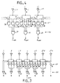
- an analog-digital converter of the "flash" type - there are other ADC structures - comprises, as very briefly recalled in FIG. 1, a first stage of comparators mounted in parallel and marked 1.2. .i, i + 1, ... 2 n -2, 2 n -1, if the ADC must supply a logic signal formed by n bits.
- the analog signal to be converted, at input E is applied in parallel to all the first comparator inputs.
- Reference voltages, by equal discrete values, are taken from a voltage divider between V min and V max and applied to the second comparator inputs.
- the set of comparators and the voltage divider forms the comparator stage, marked 3, which provides what it is used to call a thermometric scale. That is, all the comparator outputs for which the analog voltage is higher than the reference voltage provide a logic signal 1. Conversely, all the comparator outputs for which the analog voltage is lower than the reference voltage provide a logic 0 signal.
- the invention therefore consists in introducing, in an analog-digital converter, a corrector stage between the comparator stage (CAN input) and the encoder stage (CAN output).
- This corrector stage forces the output of a comparator to take the same logical value as those of the two comparators which frame it if and only if said two logical values are identical, but opposite to that provided by the comparator considered, which is accidentally erroneous .
- the correcting circuit corrects this accident and provides a logic 1. Likewise, if a logic 1 is in the middle of a series of logic 0s, the correcting circuit corrects this accident and provides a logic 0.
- the correcting circuit according to the invention is suitable for case of the two end comparators, which have only one neighbor: comparator 1 of the lightest bit, and comparator 2 n - 1 of the heaviest bit.
- the invention relates to an analog-digital converter according to claim 1.
- a parallel analog-digital converter according to the preamble is known from document US-A-4,712,087.
- thermometric scale of a CAN flash which allows the encoder 4 to determine the binary number of conversion.
- thermometric scale which is accidentally tainted with an error on an output which will be called B: the corrector stage according to the invention provides at 7 a corrected thermometric scale, whose corrected B value is correct.
- the corrector stage 5 is formed by a plurality of circuits, put in parallel, which will be suitable , to simplify writing, to call "cells".
- the correction cell corresponding to this output compares it to the output values of the two neighboring comparators, which frame it, as shown in Figure 3.
- the third column shows that there is forcing at logical 0, and the sixth column forcing at logical 1.
- the output B of comparator i is addressed to the first inputs (B) of the first and third AND gates 8 and 10.
- the output A of the comparator i + 1 is addressed to the second input (a) of the first AND gate 8 and to the first input (A) of the second AND gate 9.
- the output C of the comparator i-1 is addressed to the second input (C) of the third AND gate 10 and to the second input (C) of the second AND gate 9.
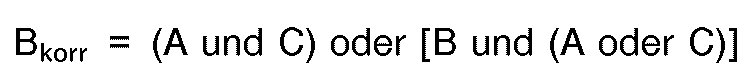
- the first AND gate 8 provides the Boolean function A.B (A and B) as an output
- the second gate 9 provides the A.C function (A and C)
- the third gate 10 provides the B.C function (B and C).
- the iterative diagram of the comparator stage 3 corresponds to an iterative diagram of the corrector stage 5, a fragment of which is represented in FIG. 4. This figure shows that the corrector stage is formed by a sub-stage of doors AND, in series with an understorey of OR doors.
- thermometric scale present a special case since they have only one neighbor.
- correction cells are shown in FIGS. 5 and 6.
- This corrector stage is applied to the realization of CAN flash, especially those which are integrated on fast materials of group III-V such as GaAs, but its diagram remains valid for slower CAN flash, on silicon, in integrated circuit or in discrete elements.
Landscapes
- Engineering & Computer Science (AREA)
- Theoretical Computer Science (AREA)
- Analogue/Digital Conversion (AREA)
Claims (6)
- Paralleler Analog-Digital-Wandler vom "Flash"-Typ, mit einer ersten Stufe (3), die aus einer Mehrzahl von Komparatoren (1 bis 2n-1) in Parallelschaltung besteht und einen an einen gemeinsamen Eingang (E) angelegten Analogwert in einen aus einer Folge von logischen 1 und einer anschließenden Folge von logischen 0 bestehenden Digitalwert verwandelt, Thermometerskala (6) genannt, und mit einer zweiten Stufe (4), Kodierstufe genannt, die die Werte der Thermometerskala (6) in eine Binärzahl verwandelt, dadurch gekennzeichnet, daß der Wandler außerdem zwischen der ersten (3) und der zweiten Stufe (4) eine dritte Stufe (5), Korrekturstufe genannt, enthält, deren Aufgabe es ist, den Wert am Ausgang B eines Komparators des Rangs "i" zu korrigieren, der versehentlich fehlerhaft ist und eine Anomalie der Thermometerskala (6) bezüglich der Ausgangswerte A und C der beiden benachbarten Komparatoren des Rangs i-1 und i+1 darstellt, wobei diese Korrekturstufe (5) den Ausgang B des Komparators des Rangs i denselben korrigierten Wert Bkorr annehmen läßt, wie die Ausgänge A und C der beiden Komparatoren des Rangs i+1 und i-1, wenn und nur wenn diese beiden Ausgangswerte A und C gleich sind und dem Wert des Ausgangs B des Komparators des Rangs i entgegengesetzt sind, so daß die Boole'sche Funktion erfüllt wird:
oder

- Wandler nach Anspruch 1, dadurch gekennzeichnet, daß die Korrekturstufe (5) eine Mehrzahl von UND-Toren (8, 9, 10) in Parallelschaltung enthält, deren Ausgänge in Gruppen von drei an ein ODER-Tor (11) angeschlossen sind, das einen korrigierten Wert Bkorr liefert.
- Wandler nach Anspruch 1, dadurch gekennzeichnet, daß die Korrekturstufe (5) eine Anzahl von Korrekturzellen gleich der Anzahl von Komparatoren (1 bis 2n-1) der ersten Stufe (3) enthält, wobei der Ausgang B jedes Komparators an eine Korrekturzelle angeschlossen ist, die im Fall einer Anomalie der Temperaturskala (6) einen korrigierten Wert Bkorr liefert.
- Wandler nach Anspruch 3, in dem A, B und C Ausgangswerte von drei benachbarten Komparatoren des Rangs i+1, i und i-1 sind, dadurch gekennzeichnet, daß ein Komparator des Rangs i in der Korrekturstufe eine Korrekturzelle enthält, die besteht aus- einer Unterstufe von drei UND-Toren (8, 9, 10) in Parallelschaltung,- einer Unterstufe eines ODER-Tors (11) in Reihe mit den drei UND-Toren (8, 9, 10), die den Ausgangswert Bkorr liefert,
wobei die Ausgangswerte A, B und C der drei Komparatoren folgendermaßen angeschlossen sind: A und B an das erste UND-Tor (8), A und C an das zweite UND-Tor (9), B und C an das dritte UND-Tor (10). - Wandler nach Anspruch 3, dadurch gekennzeichnet, daß die Korrekturzelle, die dem Komparator (2n-1) höchsten Gewichts zugeordnet ist, aus einem einzigen UND-Tor (14) besteht, das an seinen Eingängen die Ausgangswerte B und C dieses Komparators (2n-1) und des Komparators (2n-2) des unmittelbar nächstniedrigeren Gewichts empfängt und eine Ausgangswert Bkorr liefert.
- Wandler nach Anspruch 3, dadurch gekennzeichnet, daß die Korrekturzelle, die dem Komparator (1) mit geringstem Gewicht zugeordnet ist, aus einem einzigen ODER-Tor (15) besteht, das an seinen Eingängen die Ausgangswerte B und A dieses Komparators (1) und des Komparators (2) mit dem nächsthöheren Gewicht empfängt und einen Ausgangswert Bkorr liefert.
Applications Claiming Priority (2)
| Application Number | Priority Date | Filing Date | Title |
|---|---|---|---|
| FR8813539 | 1988-10-14 | ||
| FR8813539A FR2638037B1 (fr) | 1988-10-14 | 1988-10-14 | Convertisseur analogique-numerique parallele, a circuit de correction d'erreur |
Publications (2)
| Publication Number | Publication Date |
|---|---|
| EP0366517A1 EP0366517A1 (de) | 1990-05-02 |
| EP0366517B1 true EP0366517B1 (de) | 1994-04-20 |
Family
ID=9371027
Family Applications (1)
| Application Number | Title | Priority Date | Filing Date |
|---|---|---|---|
| EP89402785A Expired - Lifetime EP0366517B1 (de) | 1988-10-14 | 1989-10-10 | Paralleler Analog-Digitalwandler mit Fehlerkorrekturschaltung |
Country Status (5)
| Country | Link |
|---|---|
| US (1) | US4983968A (de) |
| EP (1) | EP0366517B1 (de) |
| JP (1) | JPH02211719A (de) |
| DE (1) | DE68914777T2 (de) |
| FR (1) | FR2638037B1 (de) |
Families Citing this family (7)
| Publication number | Priority date | Publication date | Assignee | Title |
|---|---|---|---|---|
| US5237326A (en) * | 1989-02-02 | 1993-08-17 | Samsung Electronics Co., Ltd. | Flash type analog-to-digital converter having MOS comparators |
| JP2814963B2 (ja) * | 1995-08-14 | 1998-10-27 | 日本電気株式会社 | Ad変換器 |
| US5781132A (en) * | 1996-01-17 | 1998-07-14 | Brooktree Corporation | Error correcting decoder |
| US6034631A (en) * | 1998-02-04 | 2000-03-07 | Lucent Technologies Inc. | Comparator error correction in flash analog-to-digital converter |
| JP3339566B2 (ja) * | 1998-10-21 | 2002-10-28 | 日本電気株式会社 | サーモメトリック−バイナリコード変換方法および回路、それに使用されるエンコーダ素子回路 |
| DE10060159A1 (de) * | 2000-12-04 | 2002-06-13 | Infineon Technologies Ag | Analog-Digital-Wandler und Verfahren zur Wandlung eines Analogsignals in ein Digitalsignal |
| GB2486455A (en) * | 2010-12-15 | 2012-06-20 | St Microelectronics Res & Dev | Error correction in thermometer codes |
Family Cites Families (8)
| Publication number | Priority date | Publication date | Assignee | Title |
|---|---|---|---|---|
| US3537101A (en) * | 1967-01-04 | 1970-10-27 | Us Army | High speed analog-to-digital encoder |
| US3611350A (en) * | 1970-02-12 | 1971-10-05 | Us Navy | High-speed parallel analog-to-digital converter |
| JPS5871726A (ja) * | 1981-10-26 | 1983-04-28 | Nec Corp | アナログ−デジタル変換器 |
| JPS59171315A (ja) * | 1983-03-18 | 1984-09-27 | Nec Corp | アナログ−デジタル変換器 |
| US4586025A (en) * | 1985-10-04 | 1986-04-29 | Tektronix, Inc. | Error tolerant thermometer-to-binary encoder |
| US4712087A (en) * | 1987-02-09 | 1987-12-08 | Tektronix, Inc. | Analog-to-digital converter error correction circuit |
| US4884075A (en) * | 1988-05-19 | 1989-11-28 | Analog Devices, Inc. | Decoding circuit for flash-type analog-to-digital converter |
| US4897657A (en) * | 1988-06-13 | 1990-01-30 | Integrated Device Technology, Inc. | Analog-to-digital converter having error detection and correction |
-
1988
- 1988-10-14 FR FR8813539A patent/FR2638037B1/fr not_active Expired - Fee Related
-
1989
- 1989-10-10 EP EP89402785A patent/EP0366517B1/de not_active Expired - Lifetime
- 1989-10-10 DE DE68914777T patent/DE68914777T2/de not_active Expired - Fee Related
- 1989-10-10 US US07/418,538 patent/US4983968A/en not_active Expired - Fee Related
- 1989-10-16 JP JP1268859A patent/JPH02211719A/ja active Pending
Also Published As
| Publication number | Publication date |
|---|---|
| EP0366517A1 (de) | 1990-05-02 |
| US4983968A (en) | 1991-01-08 |
| DE68914777T2 (de) | 1994-08-11 |
| FR2638037A1 (fr) | 1990-04-20 |
| JPH02211719A (ja) | 1990-08-23 |
| FR2638037B1 (fr) | 1994-04-08 |
| DE68914777D1 (de) | 1994-05-26 |
Similar Documents
| Publication | Publication Date | Title |
|---|---|---|
| US7256725B2 (en) | Resistor ladder interpolation for subranging ADC | |
| US11316526B1 (en) | Piecewise calibration for highly non-linear multi-stage analog-to-digital converter | |
| US5272481A (en) | Successive approximation analog to digital converter employing plural feedback digital to analog converters | |
| US8094056B2 (en) | Analog-to-digital converter | |
| US7808417B2 (en) | Analog-to-digital converter | |
| EP0366517B1 (de) | Paralleler Analog-Digitalwandler mit Fehlerkorrekturschaltung | |
| US6426715B1 (en) | Digital to analog converter | |
| JPH11103253A (ja) | アナログ−デジタル変換器 | |
| US5389929A (en) | Two-step subranging analog-to-digital converter | |
| US20120146821A1 (en) | Pipelined analog digital convertor | |
| US6222478B1 (en) | Pipeline analog-to-digital conversion system using a modified coding scheme and method of operation | |
| US7271755B2 (en) | Resistor ladder interpolation for PGA and DAC | |
| US6515611B1 (en) | Multistage analog-to-digital converter with amplifier component swapping for improved linearity | |
| US6784818B2 (en) | Analog to digital converter with interpolation of reference ladder | |
| US6304204B1 (en) | Error correction architecture for pipeline analog to digital converters | |
| US7158066B2 (en) | Pipelined analog-to-digital converter having enhanced high frequency performance characteristics | |
| KR20020047041A (ko) | 디지털-아날로그 변환기 | |
| US20220190840A1 (en) | Analog-to-digital converter | |
| US6570522B1 (en) | Differential interpolated analog to digital converter | |
| EP0817390B1 (de) | Analog-Digital-Wandler | |
| EP0309365B1 (de) | Einstellbare Stromquelle und ein digital-analoger Wandler mit automatischer Eichung und Verwendung einer solchen Quelle | |
| JP2995599B2 (ja) | アナログデジタル変換方法 | |
| US5367202A (en) | Voltage reference ladder having improved linearity | |
| US7554470B2 (en) | Self-calibrating pipeline analog-to-digital converter and method of calibrating a pipeline analog-to-digital converter | |
| FR2648643A1 (fr) | Circuit d'interface entre deux circuits numeriques de natures differentes |
Legal Events
| Date | Code | Title | Description |
|---|---|---|---|
| PUAI | Public reference made under article 153(3) epc to a published international application that has entered the european phase |
Free format text: ORIGINAL CODE: 0009012 |
|
| AK | Designated contracting states |
Kind code of ref document: A1 Designated state(s): DE GB NL |
|
| 17P | Request for examination filed |
Effective date: 19900518 |
|
| 17Q | First examination report despatched |
Effective date: 19930831 |
|
| RAP1 | Party data changed (applicant data changed or rights of an application transferred) |
Owner name: THOMSON-CSF SEMICONDUCTEURS SPECIFIQUES |
|
| GRAA | (expected) grant |
Free format text: ORIGINAL CODE: 0009210 |
|
| AK | Designated contracting states |
Kind code of ref document: B1 Designated state(s): DE GB NL |
|
| REF | Corresponds to: |
Ref document number: 68914777 Country of ref document: DE Date of ref document: 19940526 |
|
| GBT | Gb: translation of ep patent filed (gb section 77(6)(a)/1977) |
Effective date: 19940609 |
|
| PLBE | No opposition filed within time limit |
Free format text: ORIGINAL CODE: 0009261 |
|
| STAA | Information on the status of an ep patent application or granted ep patent |
Free format text: STATUS: NO OPPOSITION FILED WITHIN TIME LIMIT |
|
| 26N | No opposition filed | ||
| PGFP | Annual fee paid to national office [announced via postgrant information from national office to epo] |
Ref country code: NL Payment date: 19950915 Year of fee payment: 7 |
|
| PGFP | Annual fee paid to national office [announced via postgrant information from national office to epo] |
Ref country code: GB Payment date: 19950920 Year of fee payment: 7 |
|
| PGFP | Annual fee paid to national office [announced via postgrant information from national office to epo] |
Ref country code: DE Payment date: 19950923 Year of fee payment: 7 |
|
| PG25 | Lapsed in a contracting state [announced via postgrant information from national office to epo] |
Ref country code: GB Effective date: 19961010 |
|
| PG25 | Lapsed in a contracting state [announced via postgrant information from national office to epo] |
Ref country code: NL Effective date: 19970501 |
|
| GBPC | Gb: european patent ceased through non-payment of renewal fee |
Effective date: 19961010 |
|
| NLV4 | Nl: lapsed or anulled due to non-payment of the annual fee |
Effective date: 19970501 |
|
| PG25 | Lapsed in a contracting state [announced via postgrant information from national office to epo] |
Ref country code: DE Effective date: 19970701 |