EP0367004B1 - Abscheidung von Silizium enthaltenden Filmen unter Verwendung von Organosilizium-Verbindungen und Stickstofftrifluorid - Google Patents
Abscheidung von Silizium enthaltenden Filmen unter Verwendung von Organosilizium-Verbindungen und Stickstofftrifluorid Download PDFInfo
- Publication number
- EP0367004B1 EP0367004B1 EP89119151A EP89119151A EP0367004B1 EP 0367004 B1 EP0367004 B1 EP 0367004B1 EP 89119151 A EP89119151 A EP 89119151A EP 89119151 A EP89119151 A EP 89119151A EP 0367004 B1 EP0367004 B1 EP 0367004B1
- Authority
- EP
- European Patent Office
- Prior art keywords
- chamber
- compound
- nitrogen trifluoride
- introducing
- silicon
- Prior art date
- Legal status (The legal status is an assumption and is not a legal conclusion. Google has not performed a legal analysis and makes no representation as to the accuracy of the status listed.)
- Expired - Lifetime
Links
- QKCGXXHCELUCKW-UHFFFAOYSA-N n-[4-[4-(dinaphthalen-2-ylamino)phenyl]phenyl]-n-naphthalen-2-ylnaphthalen-2-amine Chemical compound C1=CC=CC2=CC(N(C=3C=CC(=CC=3)C=3C=CC(=CC=3)N(C=3C=C4C=CC=CC4=CC=3)C=3C=C4C=CC=CC4=CC=3)C3=CC4=CC=CC=C4C=C3)=CC=C21 QKCGXXHCELUCKW-UHFFFAOYSA-N 0.000 title claims description 35
- 150000003961 organosilicon compounds Chemical class 0.000 title claims description 12
- 230000008021 deposition Effects 0.000 title description 44
- XUIMIQQOPSSXEZ-UHFFFAOYSA-N Silicon Chemical group [Si] XUIMIQQOPSSXEZ-UHFFFAOYSA-N 0.000 title description 5
- 229910052710 silicon Inorganic materials 0.000 title description 5
- 239000010703 silicon Substances 0.000 title description 5
- 238000000151 deposition Methods 0.000 claims description 54
- BOTDANWDWHJENH-UHFFFAOYSA-N Tetraethyl orthosilicate Chemical compound CCO[Si](OCC)(OCC)OCC BOTDANWDWHJENH-UHFFFAOYSA-N 0.000 claims description 33
- 238000000034 method Methods 0.000 claims description 27
- QVGXLLKOCUKJST-UHFFFAOYSA-N atomic oxygen Chemical compound [O] QVGXLLKOCUKJST-UHFFFAOYSA-N 0.000 claims description 23
- 239000001301 oxygen Substances 0.000 claims description 23
- 229910052760 oxygen Inorganic materials 0.000 claims description 23
- 150000001875 compounds Chemical class 0.000 claims description 10
- 238000004518 low pressure chemical vapour deposition Methods 0.000 claims description 9
- 239000000203 mixture Substances 0.000 claims description 9
- 239000007789 gas Substances 0.000 claims description 8
- 239000002210 silicon-based material Substances 0.000 claims description 8
- 239000007788 liquid Substances 0.000 claims description 5
- 229910052581 Si3N4 Inorganic materials 0.000 claims description 4
- 125000005375 organosiloxane group Chemical group 0.000 claims description 3
- HQVNEWCFYHHQES-UHFFFAOYSA-N silicon nitride Chemical compound N12[Si]34N5[Si]62N3[Si]51N64 HQVNEWCFYHHQES-UHFFFAOYSA-N 0.000 claims description 3
- KOJCPAMHGPVAEW-UHFFFAOYSA-N 2,4,6,8-tetraethyl-1,3,5,7,2,4,6,8-tetraoxatetrasilocane Chemical compound CC[SiH]1O[SiH](CC)O[SiH](CC)O[SiH](CC)O1 KOJCPAMHGPVAEW-UHFFFAOYSA-N 0.000 claims description 2
- 239000000758 substrate Substances 0.000 claims description 2
- 230000001105 regulatory effect Effects 0.000 claims 2
- 230000005587 bubbling Effects 0.000 claims 1
- QJGQUHMNIGDVPM-UHFFFAOYSA-N nitrogen group Chemical group [N] QJGQUHMNIGDVPM-UHFFFAOYSA-N 0.000 claims 1
- 150000002894 organic compounds Chemical class 0.000 claims 1
- 230000008016 vaporization Effects 0.000 claims 1
- VYPSYNLAJGMNEJ-UHFFFAOYSA-N Silicium dioxide Chemical group O=[Si]=O VYPSYNLAJGMNEJ-UHFFFAOYSA-N 0.000 description 24
- 238000002474 experimental method Methods 0.000 description 23
- 239000010408 film Substances 0.000 description 16
- GVGCUCJTUSOZKP-UHFFFAOYSA-N nitrogen trifluoride Chemical compound FN(F)F GVGCUCJTUSOZKP-UHFFFAOYSA-N 0.000 description 15
- YCKRFDGAMUMZLT-UHFFFAOYSA-N Fluorine atom Chemical compound [F] YCKRFDGAMUMZLT-UHFFFAOYSA-N 0.000 description 13
- 229910052731 fluorine Inorganic materials 0.000 description 12
- 239000011737 fluorine Substances 0.000 description 12
- 239000000377 silicon dioxide Substances 0.000 description 12
- 235000012239 silicon dioxide Nutrition 0.000 description 12
- 238000000623 plasma-assisted chemical vapour deposition Methods 0.000 description 11
- WZJUBBHODHNQPW-UHFFFAOYSA-N 2,4,6,8-tetramethyl-1,3,5,7,2$l^{3},4$l^{3},6$l^{3},8$l^{3}-tetraoxatetrasilocane Chemical compound C[Si]1O[Si](C)O[Si](C)O[Si](C)O1 WZJUBBHODHNQPW-UHFFFAOYSA-N 0.000 description 8
- 210000002381 plasma Anatomy 0.000 description 8
- 239000000376 reactant Substances 0.000 description 8
- IJGRMHOSHXDMSA-UHFFFAOYSA-N Atomic nitrogen Chemical compound N#N IJGRMHOSHXDMSA-UHFFFAOYSA-N 0.000 description 6
- ABTOQLMXBSRXSM-UHFFFAOYSA-N silicon tetrafluoride Chemical compound F[Si](F)(F)F ABTOQLMXBSRXSM-UHFFFAOYSA-N 0.000 description 5
- GQPLMRYTRLFLPF-UHFFFAOYSA-N Nitrous Oxide Chemical compound [O-][N+]#N GQPLMRYTRLFLPF-UHFFFAOYSA-N 0.000 description 4
- 125000000217 alkyl group Chemical group 0.000 description 4
- TXEYQDLBPFQVAA-UHFFFAOYSA-N tetrafluoromethane Chemical compound FC(F)(F)F TXEYQDLBPFQVAA-UHFFFAOYSA-N 0.000 description 4
- 229910004014 SiF4 Inorganic materials 0.000 description 3
- BLRPTPMANUNPDV-UHFFFAOYSA-N Silane Chemical compound [SiH4] BLRPTPMANUNPDV-UHFFFAOYSA-N 0.000 description 3
- 238000006243 chemical reaction Methods 0.000 description 3
- 229910052681 coesite Inorganic materials 0.000 description 3
- 229910052906 cristobalite Inorganic materials 0.000 description 3
- 238000000354 decomposition reaction Methods 0.000 description 3
- 230000000694 effects Effects 0.000 description 3
- 229910052757 nitrogen Inorganic materials 0.000 description 3
- 238000005001 rutherford backscattering spectroscopy Methods 0.000 description 3
- 229910000077 silane Inorganic materials 0.000 description 3
- 229910052682 stishovite Inorganic materials 0.000 description 3
- 229910052905 tridymite Inorganic materials 0.000 description 3
- QGZKDVFQNNGYKY-UHFFFAOYSA-N Ammonia Chemical compound N QGZKDVFQNNGYKY-UHFFFAOYSA-N 0.000 description 2
- XKRFYHLGVUSROY-UHFFFAOYSA-N Argon Chemical compound [Ar] XKRFYHLGVUSROY-UHFFFAOYSA-N 0.000 description 2
- 239000000654 additive Substances 0.000 description 2
- 230000000996 additive effect Effects 0.000 description 2
- 239000011261 inert gas Substances 0.000 description 2
- 150000002500 ions Chemical class 0.000 description 2
- 229910052751 metal Inorganic materials 0.000 description 2
- 239000002184 metal Substances 0.000 description 2
- 239000001272 nitrous oxide Substances 0.000 description 2
- 229910021420 polycrystalline silicon Inorganic materials 0.000 description 2
- 229920005591 polysilicon Polymers 0.000 description 2
- 239000011541 reaction mixture Substances 0.000 description 2
- OPSKRIKFYGJQGJ-UHFFFAOYSA-N 2,4,6,8-tetraethyl-1,3,5,7,2$l^{3},4$l^{3},6$l^{3},8$l^{3}-tetraoxatetrasilocane Chemical compound CC[Si]1O[Si](CC)O[Si](CC)O[Si](CC)O1 OPSKRIKFYGJQGJ-UHFFFAOYSA-N 0.000 description 1
- OKTJSMMVPCPJKN-UHFFFAOYSA-N Carbon Chemical compound [C] OKTJSMMVPCPJKN-UHFFFAOYSA-N 0.000 description 1
- UGFAIRIUMAVXCW-UHFFFAOYSA-N Carbon monoxide Chemical compound [O+]#[C-] UGFAIRIUMAVXCW-UHFFFAOYSA-N 0.000 description 1
- UFHFLCQGNIYNRP-UHFFFAOYSA-N Hydrogen Chemical compound [H][H] UFHFLCQGNIYNRP-UHFFFAOYSA-N 0.000 description 1
- 229910021529 ammonia Inorganic materials 0.000 description 1
- 229910052786 argon Inorganic materials 0.000 description 1
- 230000015572 biosynthetic process Effects 0.000 description 1
- 229910052799 carbon Inorganic materials 0.000 description 1
- 229910002091 carbon monoxide Inorganic materials 0.000 description 1
- 239000012159 carrier gas Substances 0.000 description 1
- 238000004140 cleaning Methods 0.000 description 1
- 230000002860 competitive effect Effects 0.000 description 1
- 230000003247 decreasing effect Effects 0.000 description 1
- 238000010586 diagram Methods 0.000 description 1
- 238000000605 extraction Methods 0.000 description 1
- 239000012634 fragment Substances 0.000 description 1
- 239000001307 helium Substances 0.000 description 1
- 229910052734 helium Inorganic materials 0.000 description 1
- SWQJXJOGLNCZEY-UHFFFAOYSA-N helium atom Chemical compound [He] SWQJXJOGLNCZEY-UHFFFAOYSA-N 0.000 description 1
- 239000001257 hydrogen Substances 0.000 description 1
- 229910052739 hydrogen Inorganic materials 0.000 description 1
- 125000002887 hydroxy group Chemical group [H]O* 0.000 description 1
- 238000011065 in-situ storage Methods 0.000 description 1
- 238000004433 infrared transmission spectrum Methods 0.000 description 1
- 230000006911 nucleation Effects 0.000 description 1
- 238000010899 nucleation Methods 0.000 description 1
- 230000003647 oxidation Effects 0.000 description 1
- 238000007254 oxidation reaction Methods 0.000 description 1
- 239000010409 thin film Substances 0.000 description 1
Images

Classifications
-
- C—CHEMISTRY; METALLURGY
- C23—COATING METALLIC MATERIAL; COATING MATERIAL WITH METALLIC MATERIAL; CHEMICAL SURFACE TREATMENT; DIFFUSION TREATMENT OF METALLIC MATERIAL; COATING BY VACUUM EVAPORATION, BY SPUTTERING, BY ION IMPLANTATION OR BY CHEMICAL VAPOUR DEPOSITION, IN GENERAL; INHIBITING CORROSION OF METALLIC MATERIAL OR INCRUSTATION IN GENERAL
- C23C—COATING METALLIC MATERIAL; COATING MATERIAL WITH METALLIC MATERIAL; SURFACE TREATMENT OF METALLIC MATERIAL BY DIFFUSION INTO THE SURFACE, BY CHEMICAL CONVERSION OR SUBSTITUTION; COATING BY VACUUM EVAPORATION, BY SPUTTERING, BY ION IMPLANTATION OR BY CHEMICAL VAPOUR DEPOSITION, IN GENERAL
- C23C16/00—Chemical coating by decomposition of gaseous compounds, without leaving reaction products of surface material in the coating, i.e. chemical vapour deposition [CVD] processes
- C23C16/22—Chemical coating by decomposition of gaseous compounds, without leaving reaction products of surface material in the coating, i.e. chemical vapour deposition [CVD] processes characterised by the deposition of inorganic material, other than metallic material
- C23C16/30—Deposition of compounds, mixtures or solid solutions, e.g. borides, carbides, nitrides
- C23C16/40—Oxides
- C23C16/401—Oxides containing silicon
- C23C16/402—Silicon dioxide
-
- Y—GENERAL TAGGING OF NEW TECHNOLOGICAL DEVELOPMENTS; GENERAL TAGGING OF CROSS-SECTIONAL TECHNOLOGIES SPANNING OVER SEVERAL SECTIONS OF THE IPC; TECHNICAL SUBJECTS COVERED BY FORMER USPC CROSS-REFERENCE ART COLLECTIONS [XRACs] AND DIGESTS
- Y10—TECHNICAL SUBJECTS COVERED BY FORMER USPC
- Y10S—TECHNICAL SUBJECTS COVERED BY FORMER USPC CROSS-REFERENCE ART COLLECTIONS [XRACs] AND DIGESTS
- Y10S148/00—Metal treatment
- Y10S148/114—Nitrides of silicon
-
- Y—GENERAL TAGGING OF NEW TECHNOLOGICAL DEVELOPMENTS; GENERAL TAGGING OF CROSS-SECTIONAL TECHNOLOGIES SPANNING OVER SEVERAL SECTIONS OF THE IPC; TECHNICAL SUBJECTS COVERED BY FORMER USPC CROSS-REFERENCE ART COLLECTIONS [XRACs] AND DIGESTS
- Y10—TECHNICAL SUBJECTS COVERED BY FORMER USPC
- Y10S—TECHNICAL SUBJECTS COVERED BY FORMER USPC CROSS-REFERENCE ART COLLECTIONS [XRACs] AND DIGESTS
- Y10S148/00—Metal treatment
- Y10S148/118—Oxide films
Definitions
- TEOS tetraethoxysilane
- LPCVD low pressure chemical vapor deposition
- PECVD plasma-enhanced chemical vapor deposition
- the overall decomposition reaction can, in general, be represented by the following equation: If this oxidation process is incomplete, carbon monoxide may also be a product and the resulting oxide films may contain mobile ions such as carbon, hydroxyl and silicon-hydrogen groups.
- the compressive stress of silicon dioxide films using silane and nitrous oxide can be reduced by the addition of small amounts of fluorine-containing compounds such as CF4, SiF4, and NF3.
- fluorine-containing compounds such as CF4, SiF4, and NF3.
- SiF4 the deposition rate increased with increasing flow of the additive while with NF3 the rate decreased.
- PECVD plasma-enhanced chemical vapor deposition
- One aspect of the present invention comprises a process for depositing a layer of a silicon-containing compound on a wafer and a composition as defined in claim 1.
- the wafer is disposed in a chamber evacuated to a low pressure, such as a pressure less than about 1064 N/m2 (eight torr).
- a low pressure such as a pressure less than about 1064 N/m2 (eight torr).
- At least two gas reactants are introduced to the chamber, including a gaseous organosilicon compound and nitrogen trifluoride. These reactants will deposit the silicon-containing compound on the wafer at a rate that is enhanced over the deposition rate that would be obtained without using nitrogen trifluoride.
- the enhancement of the deposition rate with the use of nitrogen trifluoride is a surprising result.
- the above process has application to the deposition of silicon dioxide, silicon nitride and polysilicon.
- the organosilicon compound comprise an organosiloxane such as tetraethoxysilane (TEOS) or an alkyl cyclosiloxane such as tetraethylcyclotetrasiloxane or tetramethylcyclotetrasiloxane.
- TEOS tetraethoxysilane
- alkyl cyclosiloxane such as tetraethylcyclotetrasiloxane or tetramethylcyclotetrasiloxane.
- oxygen be introduced into the chamber together with the organosilicon compound and nitrogen trifluoride reactant, as further enhancements in the deposition rate have been observed with this additive.
- the oxygen introduced in the chamber may first be bubbled through a TEOS liquid, with vaporized TEOS being carried into the chamber by oxygen.
- the energy for the chemical reaction necessary for film deposition can be lent to the reactants through the formation of a plasma by radio frequency, microwave or magnetically enhanced techniques.
- the deposition can proceed thermally using low-pressure chemical vapor deposition (LPCVD).
- the process may be carried out at pressures below 133 N/m2 (1.0 torr) to achieve the filling of topographical features having high aspect ratios.
- Aspect ratios of topographical features filled by conventional TEOS systems measure no more than 0.7 to 0.8.
- a filling of features having aspect ratios in excess of 1.0 can be obtained with a film of good structural integrity.
- the use of NF3 as a reactant may also lower mobile ion concentration and surface-state charge density in the deposited film.
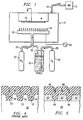
- FIGURE 1 is a schematic representation of apparatus to carry out the invention, the apparatus preferably including a plasma-enhanced chemical vapor deposition (PECVD) reactor shown generally at 10.
- Chamber 10 is hermetically sealed and is evacuated by a vacuum pump 12 connected to the interior of chamber 10 by a vacuum line 14.
- the interior of chamber 10 is evacuated to a pressure in the range from about 53,2 N/m2 (0.4 torr) to about 1064 N/m2 (8 torr).
- a wafer W is attached by clips or the like (not shown) to a grounded plate 16.
- Plate 16 is suspended over a "shower head" manifold 18 that is connected to an rf energy source 20. It is preferred that plate 16 be heated.
- the invention also has application to reactors in which a plasma is generated by other means, such as magnetically-assisted rf or microwave, and further applies to nonplasma reactors such as a low-pressure chemical vapor deposition (LPCVD) reactor.
- LPCVD low-pressure chemical vapor deposition
- a source 22 of nitrogen trifluoride is connected as by means of a tube 24 to the manifold 18.
- a tank 26 of oxygen is connected through a tube 28 to the bottom of a vessel 30 that contains an amount of tetraethoxysilane (TEOS) in liquid form.
- TEOS tetraethoxysilane
- the TEOS can be replaced with another alkyl oxysilane or an alkyl cyclosiloxane, such as 1,3,5,7 tetraethylcyclotetrasiloxane (TECTS) or 1,3,5,7 tetramethylcyclotetrasiloxane (TMCTS).
- TECTS 1,3,5,7 tetraethylcyclotetrasiloxane
- TCTS 1,3,5,7 tetramethylcyclotetrasiloxane
- the oxygen carries TEOS vapor with it through a
- the TEOS may be introduced directly into the manifold 18 as a vapor instead of being carried by the oxygen from tank 26. While it is preferred that oxygen be used in the reaction mixture, it is not absolutely essential.
- a carrier gas for the TEOS may comprise any other inert gas such as helium, argon or nitrogen. Suitable valves and meters (not shown) are used to control the flow rates of the reactants into the chamber 10.
- TEOS was introduced into a single-wafer PECVD reactor at a flow rate of approximately ten standard cubic centimeters/minute (sccm).
- the flow rate of TEOS for the last six experiments in the range of three to five sccm.
- no fluorine source was used at all.
- the power applied to the shower head electrode was 230 watts and oxygen was bubbled through the bubbler at a flow rate of about 175 sccm. Pressure was held at 266 N/m2 (two torr). The deposition rate thus achieved was 285 nm/min (2850 Angstroms per minute).
- Experiments 5 and 6 were carried out at a pressure of 399 N/m2 (three torr) with experiment 5 having no fluorine source while experiment 6 introduced nitrogen trifluoride at 32 sccm. The difference in oxide deposition rate was over 1000 nm/min (10,000 Angstroms per minute).
- Experiments 7 through 10 were conducted at a pressure of 532 N/m2 (four torr). Experiment 7 used no fluorine source at all, while experiments 8 and 9 introduced 20 sccm of tetrafluoromethane and tetrafluorosilane, respectively. As in the case of the experiments conducted at 266 N/m2 (two torr), there was little effect on the deposition rate by these two fluorine sources. Once again, as shown by Experiment 10, a substantial increase in deposition rate was noted when nitrogen trifluoride was used as the fluorine source.
- Experiments 11 through 16 were conducted at a substantially reduced pressure of 79,8 N/m2 (0.6) torr. A base deposition rate without any fluorine source was established by Experiment 11 at about 130 nm/min (1300 Angstroms) per minute. This deposition rate is too low to be competitive with batch reactors.
- Experiments 12 through 16 added increasing amounts of nitrogen trifluoride. With no oxygen, a dramatic increase in the deposition rate was recorded for nitrogen trifluoride at only 5 sccm, as is shown for Experiment 12. The addition of 5 sccm oxygen somewhat enhances the deposition rate further, as shown by Experiment 13. Further advances in deposition rate were noted by further increases in the nitrogen trifluoride flow rate.
- a deposition rate in excess of 500nm/min (5000 Angstroms per minute) were noted when the flow rate of nitrogen trifluoride was approximately 20 sccm, roughly corresponding to a molar ratio of about five to one with respect to the TEOS.
- TMCTS was used as the organosilicon gaseous compound and was introduced into the same LPCVD reactor with nitrogen trifluoride.
- An oxygen flow rate was established at 158 sccm.
- the TMCTS flow rate was metered at between four and five sccm.
- Rf power was applied to the shower head manifold at 150 watts, and the pressure was held at 73,15 N/m2 (0.55 torr).
- FIGURE 4 is a highly magnified schematic cross sectional view of a silicon wafer 50 having a plurality of trenches 52 formed therein.
- An oxide layer 54 was deposited on the wafer 50 from TEOS according to a conventional process.
- a plurality of voids 56 were formed such that the trenches 52 were not completely filled.
- the limit of aspect ratios of topographical features capable of being filled by conventional TEOS processes has been found to be in the range of 0.7 to 0.8, where the aspect ratio is calculated as the ratio of depth over width of the feature.
- the oxide layer 54 produced in FIGURE 3 was produced with a flow rate of approximately ten sccm of TEOS and 175 sccm of O2, but without any nitrogen trifluoride being introduced into the reactor.
- FIGURE 5 is a highly magnified schematic cross sectional view of a silicon substrate 50 on which a plurality of metal leads 62 have been deposited.
- a plurality of trenches 64 are formed in between the metal lead 62 that have aspect ratios of approximately 1:1.
- a layer 66 of oxide was deposited on this structure in a PECVD reactor with a flow rate of 175 sccm of oxygen, 10 sccm TEOS and 10 sccm nitrogen trifluoride. As is seen, the trenches 64 were completely filled with the oxide 66, with voids 68 only occurring well above the trenches 64.
- This enhanced capability to fill high aspect ratio features may result because the oxide deposition with NF3 is more anisotropic. Therefore, there is a reduced sidewall deposition. Aspect ratios up to at least 1.0 can be filled with oxide of good integrity, using O2 to NF3 ratios of less than about 6:1, and more preferably about 3:1.
- the present invention has general application to any deposition system using an organosilicon compound that contains an aliphatic C-H group.
- Organosilicon sources for Si3N4 and polysilicon films are chemically similar to those for the oxide thin films above discussed. Hence, the addition of NF3 to the reaction mixture is expected to enhance deposition rates for these types of films also.
- Alternative energy sources for making plasma include microwave-induced remote plasma and magnetically enhanced plasmas by magnetron or electron cyclotron resonance. Where a silicon nitride film is desired to be deposited, ammonia, nitrogen or another source of nitrogen is also introduced into the reactor to obtain the required stoichiometry.
Landscapes
- Chemical & Material Sciences (AREA)
- Inorganic Chemistry (AREA)
- General Chemical & Material Sciences (AREA)
- Chemical Kinetics & Catalysis (AREA)
- Engineering & Computer Science (AREA)
- Materials Engineering (AREA)
- Mechanical Engineering (AREA)
- Metallurgy (AREA)
- Organic Chemistry (AREA)
- Chemical Vapour Deposition (AREA)
- Formation Of Insulating Films (AREA)
Claims (19)
- Zusammensetzung zum Ablagern einer Schicht einer siliziumhaltigen Verbindung auf einem Substrat in einem Niederdruckreaktor, enthaltend:
zwischen 2 und 70 Vol.-% einer Organosilizium-Gasverbindung und
zwischen 4 und 70 Vol.- % Stickstofftrifluorid. - Zusammensetzung nach Anspruch 1, bei welcher die Organosilizium-Gasverbindung ein Organosiloxan ist.
- Zusammensetzung nach Anspruch 2, bei welcher das Organosiloxan Tetraethoxysilan ist.
- Zusammensetzung nach Anspruch 3, bei welcher das molare Verhältnis von Stickstofftrifluorid zu Tetraethoxysilan wenigstens vier zu eins beträgt.
- Zusammensetzung nach Anspruch 2, bei welcher die Organosilizium-Gasverbindung ein Alkylcyclosiloxan ist.
- Zusammensetzung nach Anspruch 2, bei welcher das Alkylcyclosiloxan ein Tetraethylcyclotetrasiloxan ist.
- Verfahren zum Ablagern einer Schicht aus einer siliziumhaltigen Verbindung auf einer Scheibe, enthaltend die Schritte:
Anbringen der Scheibe in einer auf einen niedrigen Druck evakuierten Kammer;
Einführen einer gasförmigen Organosiliziumverbindung in die Kammer;
Einführen von Stickstofftrifluorid in die Kammer;
Umsetzen der gasförmigen Organosiliziumverbindung mit dem Stickstofftrifluorid als Antwort auf die Schritte des Einführens der organischen Verbindung und des Stickstofftrifluorids in die Kammer; und
als Antwort auf den Umsetzungsschritt, Ablagern der siliziumhaltigen Verbindung auf der Scheibe mit einer Rate, die größer als eine entsprechende Ablagerungsrate ist, die ohne Verwendung von Stickstofftrifluorid erhalten wird. - Verfahren nach Anspruch 7, ferner enthaltend den Schritt des Regelns des Drucks innerhalb der Kammer so, daß er nicht mehr als etwa 532 N/m² (4 Torr) beträgt.
- Verfahren nach Anspruch 7, ferner enthaltend den Schritt des Regelns des Drucks innerhalb der Kammer so, daß er weniger als etwa 133 N/m₂ (1,0 Torr) beträgt.
- Verfahren nach Anspruch 7, ferner enthaltend den Schritt des Einführens von Sauerstoff in die Kammer.
- Verfahren nach Anspruch 10, ferner enthaltend die Schritte:
Hindurchsprudeln von Sauerstoff durch eine flüssige Organosiliziumverbindung;
Verdampfen der organischen flüssigen Verbindung in dem Sauerstoff zur Erzielung der gasförmigen Organosiliziumverbindung; und
Überführen der gasförmigen Organosiliziumverbindung in die Kammer mit dem Sauerstoff. - Verfahren nach Anspruch 7, ferner enthaltend den Schritt des Erzeugens eines Plasmas zur Erzielung der Reaktion der eingeführten Gase.
- Verfahren nach Anspruch 7, ferner enthaltend den Schritt des Ablagerns der siliziumhaltigen Verbindung unter Verwendung der chemischen Dampfabscheidung bei niedrigem Druck.
- Verfahren nach Anspruch 7, ferner enthaltend die Schritte:
Einführen des Stickstofftrifuorids in die Kammer in Mengen, die von 4 bis 70 Vol.-% reichen; und
Einführen der gasförmigen Organosiliziumverbindung in die Kammer in Mengen, die von 2 bis 70 Vol.-% erreichen. - Verfahren nach Anspruch 7, ferner enthaltend die Schritte:
Einführen eines zweiten stickstoffhaltigen Gases in die Kammer; und
Ablagern der Schicht auf der Scheibe so, daß sie Siliziumnitrid enthält. - Verfahren zum Ablagern einer Schicht aus einer siliziumhaltigen Verbindung auf einer Scheibenoberfläche, die topographische Merkmale mit hohem Schlankheitsverhältnis haben, enthaltend die Schritte:
Anbringen der Scheibe in einer Kammer, die auf einen Druck unterhalb etwa 135 N/m² (1 Torr) evakuiert ist;
Einführen einer gasförmigen Organosiliziumverbindung in die Kammer;
Einführen von Stickstofftrifluorid in die Kammer; und
Umsetzen der Organosiliziumverbindung mit dem Stickstofftrifluorid zum Ablagern der Schicht aus der siliziumhaltigen Verbindung auf der Oberfläche so, daß in der Schicht keine Lücken gebildet werden. - Verfahren nach Anspruch 16, ferner enthaltend den Schritt des Ausfüllens topographischer Merkmale auf der Scheibe, die ein Schlankheitsverhältnis größer oder gleich 1,0 haben.
- Verfahren nach Anspruch 16, ferner enthaltend den Schritt des Einführens von Sauerstoff in die Kammer.
- Verfahren nach Anspruch 16, ferner enthaltend den Schritt des Einführens von Sauerstoff und von Stickstofftrifluorid in die Kammer in einem Volumenverhältnis, das sechs zu eins nicht überschreitet.
Applications Claiming Priority (2)
| Application Number | Priority Date | Filing Date | Title |
|---|---|---|---|
| US263162 | 1988-10-26 | ||
| US07/263,162 US4894352A (en) | 1988-10-26 | 1988-10-26 | Deposition of silicon-containing films using organosilicon compounds and nitrogen trifluoride |
Publications (2)
| Publication Number | Publication Date |
|---|---|
| EP0367004A1 EP0367004A1 (de) | 1990-05-09 |
| EP0367004B1 true EP0367004B1 (de) | 1993-12-15 |
Family
ID=23000656
Family Applications (1)
| Application Number | Title | Priority Date | Filing Date |
|---|---|---|---|
| EP89119151A Expired - Lifetime EP0367004B1 (de) | 1988-10-26 | 1989-10-16 | Abscheidung von Silizium enthaltenden Filmen unter Verwendung von Organosilizium-Verbindungen und Stickstofftrifluorid |
Country Status (4)
| Country | Link |
|---|---|
| US (1) | US4894352A (de) |
| EP (1) | EP0367004B1 (de) |
| JP (1) | JP2848647B2 (de) |
| DE (1) | DE68911478T2 (de) |
Cited By (2)
| Publication number | Priority date | Publication date | Assignee | Title |
|---|---|---|---|---|
| US6905981B1 (en) | 2000-11-24 | 2005-06-14 | Asm Japan K.K. | Low-k dielectric materials and processes |
| US7144620B2 (en) | 2000-02-08 | 2006-12-05 | Asm Japan K.K. | Process for depositing low dielectric constant materials |
Families Citing this family (206)
| Publication number | Priority date | Publication date | Assignee | Title |
|---|---|---|---|---|
| KR910003742B1 (ko) * | 1986-09-09 | 1991-06-10 | 세미콘덕터 에너지 라보라터리 캄파니 리미티드 | Cvd장치 |
| US5028566A (en) * | 1987-04-10 | 1991-07-02 | Air Products And Chemicals, Inc. | Method of forming silicon dioxide glass films |
| US5013691A (en) * | 1989-07-31 | 1991-05-07 | At&T Bell Laboratories | Anisotropic deposition of silicon dioxide |
| EP0419053B1 (de) * | 1989-08-31 | 1997-12-29 | AT&T Corp. | Methode und Vorrichtung zur Ablagerung einer isolierten Schicht |
| JPH03198338A (ja) * | 1989-12-27 | 1991-08-29 | Handotai Process Kenkyusho:Kk | 気相成長膜の形成方法および半導体装置 |
| US5328872A (en) * | 1989-12-29 | 1994-07-12 | At&T Bell Laboratories | Method of integrated circuit manufacturing using deposited oxide |
| US5132774A (en) * | 1990-02-05 | 1992-07-21 | Mitsubishi Denki Kabushiki Kaisha | Semiconductor device including interlayer insulating film |
| EP0445535B1 (de) | 1990-02-06 | 1995-02-01 | Sel Semiconductor Energy Laboratory Co., Ltd. | Verfahren zum Herstellen eines Oxydfilms |
| US5120680A (en) * | 1990-07-19 | 1992-06-09 | At&T Bell Laboratories | Method for depositing dielectric layers |
| EP0511780A1 (de) * | 1991-04-30 | 1992-11-04 | AT&T Corp. | Herstellungsverfahren von einem flachen Dielektrikum |
| JPH04341568A (ja) * | 1991-05-16 | 1992-11-27 | Toshiba Corp | 薄膜形成方法及び薄膜形成装置 |
| JP3670277B2 (ja) * | 1991-05-17 | 2005-07-13 | ラム リサーチ コーポレーション | 低い固有応力および/または低い水素含有率をもつSiO▲X▼フィルムの堆積法 |
| JP2699695B2 (ja) * | 1991-06-07 | 1998-01-19 | 日本電気株式会社 | 化学気相成長法 |
| DE69231390D1 (de) * | 1991-06-10 | 2000-10-05 | At & T Corp | Anisotropische Ablagerung von Dielektrika |
| JPH05226480A (ja) * | 1991-12-04 | 1993-09-03 | Nec Corp | 半導体装置の製造方法 |
| JPH05251707A (ja) * | 1992-03-04 | 1993-09-28 | Koudo Eizou Gijutsu Kenkyusho:Kk | 薄膜トランジスタおよびその製造方法 |
| CN100465742C (zh) * | 1992-08-27 | 2009-03-04 | 株式会社半导体能源研究所 | 有源矩阵显示器 |
| US5753564A (en) * | 1992-11-24 | 1998-05-19 | Sumitomo Metal Industries, Ltd. | Method for forming a thin film of a silicon oxide on a silicon substrate, by BCR plasma |
| US5298587A (en) * | 1992-12-21 | 1994-03-29 | The Dow Chemical Company | Protective film for articles and method |
| US5599387A (en) * | 1993-02-16 | 1997-02-04 | Ppg Industries, Inc. | Compounds and compositions for coating glass with silicon oxide |
| US5356718A (en) * | 1993-02-16 | 1994-10-18 | Ppg Industries, Inc. | Coating apparatus, method of coating glass, compounds and compositions for coating glasss and coated glass substrates |
| US5863337A (en) * | 1993-02-16 | 1999-01-26 | Ppg Industries, Inc. | Apparatus for coating a moving glass substrate |
| KR0143873B1 (ko) * | 1993-02-19 | 1998-08-17 | 순페이 야마자끼 | 절연막 및 반도체장치 및 반도체 장치 제조방법 |
| US7465679B1 (en) | 1993-02-19 | 2008-12-16 | Semiconductor Energy Laboratory Co., Ltd. | Insulating film and method of producing semiconductor device |
| JP3637069B2 (ja) | 1993-03-12 | 2005-04-06 | 株式会社半導体エネルギー研究所 | 半導体装置の作製方法 |
| US5932286A (en) * | 1993-03-16 | 1999-08-03 | Applied Materials, Inc. | Deposition of silicon nitride thin films |
| JPH06326026A (ja) * | 1993-04-13 | 1994-11-25 | Applied Materials Inc | 半導体装置の薄膜形成方法 |
| US5434109A (en) * | 1993-04-27 | 1995-07-18 | International Business Machines Corporation | Oxidation of silicon nitride in semiconductor devices |
| US5571571A (en) * | 1993-06-16 | 1996-11-05 | Applied Materials, Inc. | Method of forming a thin film for a semiconductor device |
| US5433786A (en) * | 1993-08-27 | 1995-07-18 | The Dow Chemical Company | Apparatus for plasma enhanced chemical vapor deposition comprising shower head electrode with magnet disposed therein |
| KR100291971B1 (ko) * | 1993-10-26 | 2001-10-24 | 야마자끼 순페이 | 기판처리장치및방법과박막반도체디바이스제조방법 |
| US5840374A (en) * | 1993-12-28 | 1998-11-24 | Nihon Shinku Gijutsu Kabushiki Kaisha | Method of forming a SiO2 passivation film on a plastic substrate |
| JP3364694B2 (ja) * | 1993-12-28 | 2003-01-08 | 株式会社アルバック | 保護膜の形成方法 |
| JP2630257B2 (ja) * | 1994-06-03 | 1997-07-16 | 日本電気株式会社 | 半導体装置の製造方法 |
| US5563105A (en) * | 1994-09-30 | 1996-10-08 | International Business Machines Corporation | PECVD method of depositing fluorine doped oxide using a fluorine precursor containing a glass-forming element |
| US5766342A (en) * | 1994-10-19 | 1998-06-16 | Matsushita Electric Industrial Co., Ltd. | Method for forming silicon film and silicon film forming apparatus |
| EP0724286A1 (de) * | 1995-01-25 | 1996-07-31 | Applied Materials, Inc. | Verfahren zur Herstellung eines Dünnfilms aus Siliziumoxid für eine Halbleitervorrichtung |
| US5571576A (en) * | 1995-02-10 | 1996-11-05 | Watkins-Johnson | Method of forming a fluorinated silicon oxide layer using plasma chemical vapor deposition |
| US5635425A (en) * | 1995-05-25 | 1997-06-03 | Industrial Technology Research Institute | In-situ N2 plasma treatment for PE TEOS oxide deposition |
| US20010028922A1 (en) * | 1995-06-07 | 2001-10-11 | Sandhu Gurtej S. | High throughput ILD fill process for high aspect ratio gap fill |
| EP0759481A1 (de) * | 1995-06-23 | 1997-02-26 | Novellus Systems, Inc. | Verfahren zum Abscheiden eines stabilen Films aus fluoriertem TEOS |
| JP3979687B2 (ja) | 1995-10-26 | 2007-09-19 | アプライド マテリアルズ インコーポレイテッド | ハロゲンをドープした酸化珪素膜の膜安定性を改良する方法 |
| US5643640A (en) * | 1995-11-27 | 1997-07-01 | International Business Machines Corporation | Fluorine doped plasma enhanced phospho-silicate glass, and process |
| US6001728A (en) * | 1996-03-15 | 1999-12-14 | Applied Materials, Inc. | Method and apparatus for improving film stability of halogen-doped silicon oxide films |
| US5807785A (en) * | 1996-08-02 | 1998-09-15 | Applied Materials, Inc. | Low dielectric constant silicon dioxide sandwich layer |
| TW335511B (en) * | 1996-08-02 | 1998-07-01 | Applied Materials Inc | Stress control by fluorination of silica film |
| US5661093A (en) * | 1996-09-12 | 1997-08-26 | Applied Materials, Inc. | Method for the stabilization of halogen-doped films through the use of multiple sealing layers |
| US5827785A (en) * | 1996-10-24 | 1998-10-27 | Applied Materials, Inc. | Method for improving film stability of fluorosilicate glass films |
| US5763021A (en) * | 1996-12-13 | 1998-06-09 | Cypress Semiconductor Corporation | Method of forming a dielectric film |
| US5872065A (en) * | 1997-04-02 | 1999-02-16 | Applied Materials Inc. | Method for depositing low K SI-O-F films using SIF4 /oxygen chemistry |
| US6077786A (en) * | 1997-05-08 | 2000-06-20 | International Business Machines Corporation | Methods and apparatus for filling high aspect ratio structures with silicate glass |
| US6136685A (en) * | 1997-06-03 | 2000-10-24 | Applied Materials, Inc. | High deposition rate recipe for low dielectric constant films |
| US5937323A (en) | 1997-06-03 | 1999-08-10 | Applied Materials, Inc. | Sequencing of the recipe steps for the optimal low-k HDP-CVD processing |
| US5869149A (en) * | 1997-06-30 | 1999-02-09 | Lam Research Corporation | Method for preparing nitrogen surface treated fluorine doped silicon dioxide films |
| US6451686B1 (en) | 1997-09-04 | 2002-09-17 | Applied Materials, Inc. | Control of semiconductor device isolation properties through incorporation of fluorine in peteos films |
| US6121164A (en) * | 1997-10-24 | 2000-09-19 | Applied Materials, Inc. | Method for forming low compressive stress fluorinated ozone/TEOS oxide film |
| US6593247B1 (en) | 1998-02-11 | 2003-07-15 | Applied Materials, Inc. | Method of depositing low k films using an oxidizing plasma |
| US6287990B1 (en) | 1998-02-11 | 2001-09-11 | Applied Materials, Inc. | CVD plasma assisted low dielectric constant films |
| US6660656B2 (en) | 1998-02-11 | 2003-12-09 | Applied Materials Inc. | Plasma processes for depositing low dielectric constant films |
| US6627532B1 (en) * | 1998-02-11 | 2003-09-30 | Applied Materials, Inc. | Method of decreasing the K value in SiOC layer deposited by chemical vapor deposition |
| US6054379A (en) * | 1998-02-11 | 2000-04-25 | Applied Materials, Inc. | Method of depositing a low k dielectric with organo silane |
| US6303523B2 (en) | 1998-02-11 | 2001-10-16 | Applied Materials, Inc. | Plasma processes for depositing low dielectric constant films |
| US6159871A (en) | 1998-05-29 | 2000-12-12 | Dow Corning Corporation | Method for producing hydrogenated silicon oxycarbide films having low dielectric constant |
| US6667553B2 (en) | 1998-05-29 | 2003-12-23 | Dow Corning Corporation | H:SiOC coated substrates |
| KR100518147B1 (ko) * | 1998-06-01 | 2005-11-25 | 가부시키가이샤 아루박 | 증착장치,유기증발원및유기박막제조방법 |
| US6171945B1 (en) | 1998-10-22 | 2001-01-09 | Applied Materials, Inc. | CVD nanoporous silica low dielectric constant films |
| US6291341B1 (en) * | 1999-02-12 | 2001-09-18 | Micron Technology, Inc. | Method for PECVD deposition of selected material films |
| US6399489B1 (en) | 1999-11-01 | 2002-06-04 | Applied Materials, Inc. | Barrier layer deposition using HDP-CVD |
| US6458718B1 (en) | 2000-04-28 | 2002-10-01 | Asm Japan K.K. | Fluorine-containing materials and processes |
| US6630413B2 (en) | 2000-04-28 | 2003-10-07 | Asm Japan K.K. | CVD syntheses of silicon nitride materials |
| US6521546B1 (en) | 2000-06-14 | 2003-02-18 | Applied Materials, Inc. | Method of making a fluoro-organosilicate layer |
| US6764958B1 (en) | 2000-07-28 | 2004-07-20 | Applied Materials Inc. | Method of depositing dielectric films |
| US6573196B1 (en) | 2000-08-12 | 2003-06-03 | Applied Materials Inc. | Method of depositing organosilicate layers |
| US6335288B1 (en) | 2000-08-24 | 2002-01-01 | Applied Materials, Inc. | Gas chemistry cycling to achieve high aspect ratio gapfill with HDP-CVD |
| KR100797385B1 (ko) * | 2000-10-19 | 2008-01-24 | 로베르트 보쉬 게엠베하 | 유도 결합 플라즈마를 이용한 기판의 에칭 장치 및 방법 |
| US6531398B1 (en) | 2000-10-30 | 2003-03-11 | Applied Materials, Inc. | Method of depositing organosillicate layers |
| US6500773B1 (en) | 2000-11-27 | 2002-12-31 | Applied Materials, Inc. | Method of depositing organosilicate layers |
| KR101027485B1 (ko) | 2001-02-12 | 2011-04-06 | 에이에스엠 아메리카, 인코포레이티드 | 반도체 박막 증착을 위한 개선된 공정 |
| US6537733B2 (en) * | 2001-02-23 | 2003-03-25 | Applied Materials, Inc. | Method of depositing low dielectric constant silicon carbide layers |
| US6709721B2 (en) | 2001-03-28 | 2004-03-23 | Applied Materials Inc. | Purge heater design and process development for the improvement of low k film properties |
| US6777171B2 (en) | 2001-04-20 | 2004-08-17 | Applied Materials, Inc. | Fluorine-containing layers for damascene structures |
| US6740601B2 (en) | 2001-05-11 | 2004-05-25 | Applied Materials Inc. | HDP-CVD deposition process for filling high aspect ratio gaps |
| US6926926B2 (en) * | 2001-09-10 | 2005-08-09 | Applied Materials, Inc. | Silicon carbide deposited by high density plasma chemical-vapor deposition with bias |
| US6759327B2 (en) * | 2001-10-09 | 2004-07-06 | Applied Materials Inc. | Method of depositing low k barrier layers |
| US6656837B2 (en) * | 2001-10-11 | 2003-12-02 | Applied Materials, Inc. | Method of eliminating photoresist poisoning in damascene applications |
| US6838393B2 (en) * | 2001-12-14 | 2005-01-04 | Applied Materials, Inc. | Method for producing semiconductor including forming a layer containing at least silicon carbide and forming a second layer containing at least silicon oxygen carbide |
| US6699784B2 (en) | 2001-12-14 | 2004-03-02 | Applied Materials Inc. | Method for depositing a low k dielectric film (K>3.5) for hard mask application |
| US6890850B2 (en) * | 2001-12-14 | 2005-05-10 | Applied Materials, Inc. | Method of depositing dielectric materials in damascene applications |
| US7091137B2 (en) * | 2001-12-14 | 2006-08-15 | Applied Materials | Bi-layer approach for a hermetic low dielectric constant layer for barrier applications |
| ATE402277T1 (de) | 2002-02-05 | 2008-08-15 | Dow Global Technologies Inc | Chemische dampfphasenabscheidung auf einem substrat mittels eines korona-plasmas |
| AU2002246316A1 (en) * | 2002-04-08 | 2003-10-27 | Council Of Scientific And Industrial Research | Process for the production of neodymium-iron-boron permanent magnet alloy powder |
| US20030194496A1 (en) * | 2002-04-11 | 2003-10-16 | Applied Materials, Inc. | Methods for depositing dielectric material |
| US6858548B2 (en) * | 2002-04-18 | 2005-02-22 | Applied Materials, Inc. | Application of carbon doped silicon oxide film to flat panel industry |
| US20040018750A1 (en) * | 2002-07-02 | 2004-01-29 | Sophie Auguste J.L. | Method for deposition of nitrogen doped silicon carbide films |
| US7186630B2 (en) * | 2002-08-14 | 2007-03-06 | Asm America, Inc. | Deposition of amorphous silicon-containing films |
| US7749563B2 (en) * | 2002-10-07 | 2010-07-06 | Applied Materials, Inc. | Two-layer film for next generation damascene barrier application with good oxidation resistance |
| CA2504490C (en) * | 2002-10-31 | 2011-05-03 | Kyoraku Co., Ltd. | Impact absorbing member for vehicle |
| US6790788B2 (en) * | 2003-01-13 | 2004-09-14 | Applied Materials Inc. | Method of improving stability in low k barrier layers |
| US7081414B2 (en) * | 2003-05-23 | 2006-07-25 | Applied Materials, Inc. | Deposition-selective etch-deposition process for dielectric film gapfill |
| US7205240B2 (en) | 2003-06-04 | 2007-04-17 | Applied Materials, Inc. | HDP-CVD multistep gapfill process |
| US7030041B2 (en) * | 2004-03-15 | 2006-04-18 | Applied Materials Inc. | Adhesion improvement for low k dielectrics |
| US20050233555A1 (en) * | 2004-04-19 | 2005-10-20 | Nagarajan Rajagopalan | Adhesion improvement for low k dielectrics to conductive materials |
| US7229911B2 (en) * | 2004-04-19 | 2007-06-12 | Applied Materials, Inc. | Adhesion improvement for low k dielectrics to conductive materials |
| US20050277302A1 (en) * | 2004-05-28 | 2005-12-15 | Nguyen Son V | Advanced low dielectric constant barrier layers |
| US7229931B2 (en) * | 2004-06-16 | 2007-06-12 | Applied Materials, Inc. | Oxygen plasma treatment for enhanced HDP-CVD gapfill |
| US7229041B2 (en) * | 2004-06-30 | 2007-06-12 | Ohio Central Steel Company | Lifting lid crusher |
| US7288205B2 (en) * | 2004-07-09 | 2007-10-30 | Applied Materials, Inc. | Hermetic low dielectric constant layer for barrier applications |
| US20060021633A1 (en) * | 2004-07-27 | 2006-02-02 | Applied Materials, Inc. | Closed loop clean gas control |
| US7087536B2 (en) * | 2004-09-01 | 2006-08-08 | Applied Materials | Silicon oxide gapfill deposition using liquid precursors |
| US20060154494A1 (en) * | 2005-01-08 | 2006-07-13 | Applied Materials, Inc., A Delaware Corporation | High-throughput HDP-CVD processes for advanced gapfill applications |
| US7323391B2 (en) | 2005-01-15 | 2008-01-29 | Applied Materials, Inc. | Substrate having silicon germanium material and stressed silicon nitride layer |
| US7247582B2 (en) * | 2005-05-23 | 2007-07-24 | Applied Materials, Inc. | Deposition of tensile and compressive stressed materials |
| US7329586B2 (en) * | 2005-06-24 | 2008-02-12 | Applied Materials, Inc. | Gapfill using deposition-etch sequence |
| US7524750B2 (en) | 2006-04-17 | 2009-04-28 | Applied Materials, Inc. | Integrated process modulation (IPM) a novel solution for gapfill with HDP-CVD |
| US7501355B2 (en) * | 2006-06-29 | 2009-03-10 | Applied Materials, Inc. | Decreasing the etch rate of silicon nitride by carbon addition |
| US7939422B2 (en) * | 2006-12-07 | 2011-05-10 | Applied Materials, Inc. | Methods of thin film process |
| US20080142483A1 (en) * | 2006-12-07 | 2008-06-19 | Applied Materials, Inc. | Multi-step dep-etch-dep high density plasma chemical vapor deposition processes for dielectric gapfills |
| US8563095B2 (en) * | 2010-03-15 | 2013-10-22 | Applied Materials, Inc. | Silicon nitride passivation layer for covering high aspect ratio features |
| US9324576B2 (en) | 2010-05-27 | 2016-04-26 | Applied Materials, Inc. | Selective etch for silicon films |
| US8741778B2 (en) | 2010-12-14 | 2014-06-03 | Applied Materials, Inc. | Uniform dry etch in two stages |
| US10283321B2 (en) | 2011-01-18 | 2019-05-07 | Applied Materials, Inc. | Semiconductor processing system and methods using capacitively coupled plasma |
| US8771539B2 (en) | 2011-02-22 | 2014-07-08 | Applied Materials, Inc. | Remotely-excited fluorine and water vapor etch |
| US8999856B2 (en) | 2011-03-14 | 2015-04-07 | Applied Materials, Inc. | Methods for etch of sin films |
| US9064815B2 (en) | 2011-03-14 | 2015-06-23 | Applied Materials, Inc. | Methods for etch of metal and metal-oxide films |
| US8497211B2 (en) | 2011-06-24 | 2013-07-30 | Applied Materials, Inc. | Integrated process modulation for PSG gapfill |
| US8771536B2 (en) | 2011-08-01 | 2014-07-08 | Applied Materials, Inc. | Dry-etch for silicon-and-carbon-containing films |
| US8679982B2 (en) | 2011-08-26 | 2014-03-25 | Applied Materials, Inc. | Selective suppression of dry-etch rate of materials containing both silicon and oxygen |
| US8679983B2 (en) | 2011-09-01 | 2014-03-25 | Applied Materials, Inc. | Selective suppression of dry-etch rate of materials containing both silicon and nitrogen |
| US8927390B2 (en) | 2011-09-26 | 2015-01-06 | Applied Materials, Inc. | Intrench profile |
| US8808563B2 (en) | 2011-10-07 | 2014-08-19 | Applied Materials, Inc. | Selective etch of silicon by way of metastable hydrogen termination |
| WO2013070436A1 (en) | 2011-11-08 | 2013-05-16 | Applied Materials, Inc. | Methods of reducing substrate dislocation during gapfill processing |
| US9190341B2 (en) | 2012-06-05 | 2015-11-17 | Texas Instruments Incorporated | Lidded integrated circuit package |
| US9373517B2 (en) | 2012-08-02 | 2016-06-21 | Applied Materials, Inc. | Semiconductor processing with DC assisted RF power for improved control |
| US9034770B2 (en) | 2012-09-17 | 2015-05-19 | Applied Materials, Inc. | Differential silicon oxide etch |
| US9023734B2 (en) | 2012-09-18 | 2015-05-05 | Applied Materials, Inc. | Radical-component oxide etch |
| US9390937B2 (en) | 2012-09-20 | 2016-07-12 | Applied Materials, Inc. | Silicon-carbon-nitride selective etch |
| US9132436B2 (en) | 2012-09-21 | 2015-09-15 | Applied Materials, Inc. | Chemical control features in wafer process equipment |
| US8765574B2 (en) | 2012-11-09 | 2014-07-01 | Applied Materials, Inc. | Dry etch process |
| US8969212B2 (en) | 2012-11-20 | 2015-03-03 | Applied Materials, Inc. | Dry-etch selectivity |
| US8980763B2 (en) | 2012-11-30 | 2015-03-17 | Applied Materials, Inc. | Dry-etch for selective tungsten removal |
| US9064816B2 (en) | 2012-11-30 | 2015-06-23 | Applied Materials, Inc. | Dry-etch for selective oxidation removal |
| US9111877B2 (en) | 2012-12-18 | 2015-08-18 | Applied Materials, Inc. | Non-local plasma oxide etch |
| US8921234B2 (en) | 2012-12-21 | 2014-12-30 | Applied Materials, Inc. | Selective titanium nitride etching |
| US9018108B2 (en) | 2013-01-25 | 2015-04-28 | Applied Materials, Inc. | Low shrinkage dielectric films |
| US10256079B2 (en) | 2013-02-08 | 2019-04-09 | Applied Materials, Inc. | Semiconductor processing systems having multiple plasma configurations |
| US9362130B2 (en) | 2013-03-01 | 2016-06-07 | Applied Materials, Inc. | Enhanced etching processes using remote plasma sources |
| US9040422B2 (en) | 2013-03-05 | 2015-05-26 | Applied Materials, Inc. | Selective titanium nitride removal |
| US8801952B1 (en) | 2013-03-07 | 2014-08-12 | Applied Materials, Inc. | Conformal oxide dry etch |
| US10170282B2 (en) | 2013-03-08 | 2019-01-01 | Applied Materials, Inc. | Insulated semiconductor faceplate designs |
| US20140271097A1 (en) | 2013-03-15 | 2014-09-18 | Applied Materials, Inc. | Processing systems and methods for halide scavenging |
| US8895449B1 (en) | 2013-05-16 | 2014-11-25 | Applied Materials, Inc. | Delicate dry clean |
| US9114438B2 (en) | 2013-05-21 | 2015-08-25 | Applied Materials, Inc. | Copper residue chamber clean |
| US9493879B2 (en) | 2013-07-12 | 2016-11-15 | Applied Materials, Inc. | Selective sputtering for pattern transfer |
| US9773648B2 (en) | 2013-08-30 | 2017-09-26 | Applied Materials, Inc. | Dual discharge modes operation for remote plasma |
| US8956980B1 (en) | 2013-09-16 | 2015-02-17 | Applied Materials, Inc. | Selective etch of silicon nitride |
| US8951429B1 (en) | 2013-10-29 | 2015-02-10 | Applied Materials, Inc. | Tungsten oxide processing |
| US9236265B2 (en) | 2013-11-04 | 2016-01-12 | Applied Materials, Inc. | Silicon germanium processing |
| US9576809B2 (en) | 2013-11-04 | 2017-02-21 | Applied Materials, Inc. | Etch suppression with germanium |
| US9520303B2 (en) | 2013-11-12 | 2016-12-13 | Applied Materials, Inc. | Aluminum selective etch |
| US9245762B2 (en) | 2013-12-02 | 2016-01-26 | Applied Materials, Inc. | Procedure for etch rate consistency |
| US9117855B2 (en) | 2013-12-04 | 2015-08-25 | Applied Materials, Inc. | Polarity control for remote plasma |
| US9287095B2 (en) | 2013-12-17 | 2016-03-15 | Applied Materials, Inc. | Semiconductor system assemblies and methods of operation |
| US9263278B2 (en) | 2013-12-17 | 2016-02-16 | Applied Materials, Inc. | Dopant etch selectivity control |
| US9190293B2 (en) | 2013-12-18 | 2015-11-17 | Applied Materials, Inc. | Even tungsten etch for high aspect ratio trenches |
| US9287134B2 (en) | 2014-01-17 | 2016-03-15 | Applied Materials, Inc. | Titanium oxide etch |
| US9293568B2 (en) | 2014-01-27 | 2016-03-22 | Applied Materials, Inc. | Method of fin patterning |
| US9396989B2 (en) | 2014-01-27 | 2016-07-19 | Applied Materials, Inc. | Air gaps between copper lines |
| US9385028B2 (en) | 2014-02-03 | 2016-07-05 | Applied Materials, Inc. | Air gap process |
| US9499898B2 (en) | 2014-03-03 | 2016-11-22 | Applied Materials, Inc. | Layered thin film heater and method of fabrication |
| US9299575B2 (en) | 2014-03-17 | 2016-03-29 | Applied Materials, Inc. | Gas-phase tungsten etch |
| US9299538B2 (en) | 2014-03-20 | 2016-03-29 | Applied Materials, Inc. | Radial waveguide systems and methods for post-match control of microwaves |
| US9299537B2 (en) | 2014-03-20 | 2016-03-29 | Applied Materials, Inc. | Radial waveguide systems and methods for post-match control of microwaves |
| US9136273B1 (en) | 2014-03-21 | 2015-09-15 | Applied Materials, Inc. | Flash gate air gap |
| US9903020B2 (en) | 2014-03-31 | 2018-02-27 | Applied Materials, Inc. | Generation of compact alumina passivation layers on aluminum plasma equipment components |
| US9269590B2 (en) | 2014-04-07 | 2016-02-23 | Applied Materials, Inc. | Spacer formation |
| US9309598B2 (en) | 2014-05-28 | 2016-04-12 | Applied Materials, Inc. | Oxide and metal removal |
| US9847289B2 (en) | 2014-05-30 | 2017-12-19 | Applied Materials, Inc. | Protective via cap for improved interconnect performance |
| US9378969B2 (en) | 2014-06-19 | 2016-06-28 | Applied Materials, Inc. | Low temperature gas-phase carbon removal |
| US9406523B2 (en) | 2014-06-19 | 2016-08-02 | Applied Materials, Inc. | Highly selective doped oxide removal method |
| US9425058B2 (en) | 2014-07-24 | 2016-08-23 | Applied Materials, Inc. | Simplified litho-etch-litho-etch process |
| US9159606B1 (en) | 2014-07-31 | 2015-10-13 | Applied Materials, Inc. | Metal air gap |
| US9496167B2 (en) | 2014-07-31 | 2016-11-15 | Applied Materials, Inc. | Integrated bit-line airgap formation and gate stack post clean |
| US9378978B2 (en) | 2014-07-31 | 2016-06-28 | Applied Materials, Inc. | Integrated oxide recess and floating gate fin trimming |
| US9165786B1 (en) | 2014-08-05 | 2015-10-20 | Applied Materials, Inc. | Integrated oxide and nitride recess for better channel contact in 3D architectures |
| US9659753B2 (en) | 2014-08-07 | 2017-05-23 | Applied Materials, Inc. | Grooved insulator to reduce leakage current |
| US9553102B2 (en) | 2014-08-19 | 2017-01-24 | Applied Materials, Inc. | Tungsten separation |
| US9355856B2 (en) | 2014-09-12 | 2016-05-31 | Applied Materials, Inc. | V trench dry etch |
| US9478434B2 (en) | 2014-09-24 | 2016-10-25 | Applied Materials, Inc. | Chlorine-based hardmask removal |
| US9368364B2 (en) | 2014-09-24 | 2016-06-14 | Applied Materials, Inc. | Silicon etch process with tunable selectivity to SiO2 and other materials |
| US9613822B2 (en) | 2014-09-25 | 2017-04-04 | Applied Materials, Inc. | Oxide etch selectivity enhancement |
| US11637002B2 (en) | 2014-11-26 | 2023-04-25 | Applied Materials, Inc. | Methods and systems to enhance process uniformity |
| US9299583B1 (en) | 2014-12-05 | 2016-03-29 | Applied Materials, Inc. | Aluminum oxide selective etch |
| US10573496B2 (en) | 2014-12-09 | 2020-02-25 | Applied Materials, Inc. | Direct outlet toroidal plasma source |
| US10224210B2 (en) | 2014-12-09 | 2019-03-05 | Applied Materials, Inc. | Plasma processing system with direct outlet toroidal plasma source |
| US9502258B2 (en) | 2014-12-23 | 2016-11-22 | Applied Materials, Inc. | Anisotropic gap etch |
| US9343272B1 (en) | 2015-01-08 | 2016-05-17 | Applied Materials, Inc. | Self-aligned process |
| US11257693B2 (en) | 2015-01-09 | 2022-02-22 | Applied Materials, Inc. | Methods and systems to improve pedestal temperature control |
| US9373522B1 (en) | 2015-01-22 | 2016-06-21 | Applied Mateials, Inc. | Titanium nitride removal |
| US9449846B2 (en) | 2015-01-28 | 2016-09-20 | Applied Materials, Inc. | Vertical gate separation |
| US9728437B2 (en) | 2015-02-03 | 2017-08-08 | Applied Materials, Inc. | High temperature chuck for plasma processing systems |
| US20160225652A1 (en) | 2015-02-03 | 2016-08-04 | Applied Materials, Inc. | Low temperature chuck for plasma processing systems |
| US9691645B2 (en) | 2015-08-06 | 2017-06-27 | Applied Materials, Inc. | Bolted wafer chuck thermal management systems and methods for wafer processing systems |
| US9741593B2 (en) | 2015-08-06 | 2017-08-22 | Applied Materials, Inc. | Thermal management systems and methods for wafer processing systems |
| US9349605B1 (en) | 2015-08-07 | 2016-05-24 | Applied Materials, Inc. | Oxide etch selectivity systems and methods |
| US10504700B2 (en) | 2015-08-27 | 2019-12-10 | Applied Materials, Inc. | Plasma etching systems and methods with secondary plasma injection |
| CN114639602B (zh) * | 2020-12-15 | 2026-03-27 | 东京毅力科创株式会社 | 蚀刻方法和蚀刻装置 |
Family Cites Families (12)
| Publication number | Priority date | Publication date | Assignee | Title |
|---|---|---|---|---|
| DE2447224A1 (de) * | 1974-10-03 | 1976-04-15 | Ibm Deutschland | Verfahren zum aufwachsen von pyrolitischen siliciumdioxidschichten |
| DE2944180A1 (de) * | 1979-11-02 | 1981-05-07 | Licentia Patent-Verwaltungs-Gmbh, 6000 Frankfurt | Verfahren zum herstellen einer einen halbleiterkoerper einseitig bedeckenden isolierschicht |
| JPS59128281A (ja) * | 1982-12-29 | 1984-07-24 | 信越化学工業株式会社 | 炭化けい素被覆物の製造方法 |
| US4526631A (en) * | 1984-06-25 | 1985-07-02 | International Business Machines Corporation | Method for forming a void free isolation pattern utilizing etch and refill techniques |
| US4641420A (en) * | 1984-08-30 | 1987-02-10 | At&T Bell Laboratories | Metalization process for headless contact using deposited smoothing material |
| US4554047A (en) * | 1984-10-12 | 1985-11-19 | At&T Bell Laboratories | Downstream apparatus and technique |
| DE3679596D1 (de) * | 1985-05-22 | 1991-07-11 | Siemens Ag | Verfahren zum herstellen von mit bor und phosphor dotierten siliziumoxid-schichten fuer integrierte halbleiterschaltungen. |
| KR870000750A (ko) * | 1985-06-14 | 1987-02-20 | 이마드 마하윌리 | 이산화실리콘 필름을 화학적으로 증기피복하는 방법 |
| JPS62328A (ja) * | 1985-06-25 | 1987-01-06 | 古田 直樹 | 超音波プロ−ブ用アプリケ−タ |
| US4828369A (en) * | 1986-05-28 | 1989-05-09 | Minolta Camera Kabushiki Kaisha | Electrochromic device |
| US4737429A (en) * | 1986-06-26 | 1988-04-12 | Xerox Corporation | Layered amorphous silicon imaging members |
| US4748131A (en) * | 1987-02-06 | 1988-05-31 | The Aerospace Corporation | Method for increasing radiation hardness of MOS gate oxides |
-
1988
- 1988-10-26 US US07/263,162 patent/US4894352A/en not_active Expired - Lifetime
-
1989
- 1989-10-16 EP EP89119151A patent/EP0367004B1/de not_active Expired - Lifetime
- 1989-10-16 DE DE68911478T patent/DE68911478T2/de not_active Expired - Fee Related
- 1989-10-24 JP JP1276972A patent/JP2848647B2/ja not_active Expired - Fee Related
Non-Patent Citations (2)
| Title |
|---|
| JOURNAL OF VACUUM SCIENCE & TECHNOLOGY, section B, vol. 5, no. 6, November-December 1987, Woodbury, NY, US; F.S.BECKER et al.: "Low-pressure deposition of high-quality SiO2 films by pyrolysis of tetraethylorthosilicate" page 1555 * |
| PROCEEDINGS OF THE 3rd INTERNATIONAL SYMPOSIUM ON VLSI SCIENCE AND TECHNOLOGY, THE ELECTROCHEMICAL SOCIETY, vol. 89, no. 9, S. Broydo AND C.N. Osburns Ed., September 1989; D.A.WEBB et al.: "Silicon dioxide films produced by PEVCD of TEOS and TMCTS" page 571 * |
Cited By (3)
| Publication number | Priority date | Publication date | Assignee | Title |
|---|---|---|---|---|
| US7144620B2 (en) | 2000-02-08 | 2006-12-05 | Asm Japan K.K. | Process for depositing low dielectric constant materials |
| US7544827B2 (en) | 2000-02-08 | 2009-06-09 | Asm Japan K.K. | Process for depositing low dielectric constant materials |
| US6905981B1 (en) | 2000-11-24 | 2005-06-14 | Asm Japan K.K. | Low-k dielectric materials and processes |
Also Published As
| Publication number | Publication date |
|---|---|
| DE68911478T2 (de) | 1994-06-23 |
| JP2848647B2 (ja) | 1999-01-20 |
| JPH02236282A (ja) | 1990-09-19 |
| US4894352A (en) | 1990-01-16 |
| EP0367004A1 (de) | 1990-05-09 |
| DE68911478D1 (de) | 1994-01-27 |
Similar Documents
| Publication | Publication Date | Title |
|---|---|---|
| EP0367004B1 (de) | Abscheidung von Silizium enthaltenden Filmen unter Verwendung von Organosilizium-Verbindungen und Stickstofftrifluorid | |
| EP0440154B1 (de) | Zweistufiges Verfahren zur Herstellung einer Oxidschicht auf einer stufenförmigen Halbleiterwaferfläche | |
| EP0584252B1 (de) | VERFAHREN ZUR BESCHICHTUNG EINES SIOx FILMES MIT REDUZIERTER INTRINSISCHER SPANNUNG UND/ODER REDUZIERTEM WASSERSTOFFGEHALT | |
| US5166101A (en) | Method for forming a boron phosphorus silicate glass composite layer on a semiconductor wafer | |
| US6787483B1 (en) | Gap fill for high aspect ratio structures | |
| US7309662B1 (en) | Method and apparatus for forming a film on a substrate | |
| US6846745B1 (en) | High-density plasma process for filling high aspect ratio structures | |
| US7294556B2 (en) | Method of forming trench isolation in the fabrication of integrated circuitry | |
| US6974780B2 (en) | Semiconductor processing methods of chemical vapor depositing SiO2 on a substrate | |
| US6958112B2 (en) | Methods and systems for high-aspect-ratio gapfill using atomic-oxygen generation | |
| US6500772B2 (en) | Methods and materials for depositing films on semiconductor substrates | |
| JP3077119B2 (ja) | 二酸化ケイ素の化学気相成長法 | |
| US20040245091A1 (en) | Hdp-cvd multistep gapfill process | |
| JPH03504617A (ja) | 基板上への窒化けい素及び二酸化けい素フイルムのプラズマデポジシヨン法 | |
| WO1999027154A1 (en) | Silicon nitrogen-based films and method of making the same | |
| EP0421203B1 (de) | Integrierte Schaltungsstruktur mit einer zusammengesetzten Borphosphorsilikatglasschicht auf einer Halbleiterscheibe und verbesserte Herstellungsmethode dafür | |
| EP0212691A1 (de) | Chemisches Niederschlagen von SiO2-Filmen aus der Dampfphase bei niedriger Temperatur | |
| US7176039B1 (en) | Dynamic modification of gap fill process characteristics | |
| US5045346A (en) | Method of depositing fluorinated silicon nitride | |
| US5061514A (en) | Chemical vapor deposition (CVD) process for plasma depositing silicon carbide films onto a substrate | |
| US7067440B1 (en) | Gap fill for high aspect ratio structures | |
| JPH06168937A (ja) | シリコン酸化膜の製造方法 | |
| Horiike et al. | Filling of Si oxide into a deep trench using digital CVD method | |
| US7122485B1 (en) | Deposition profile modification through process chemistry | |
| US5849644A (en) | Semiconductor processing methods of chemical vapor depositing SiO2 on a substrate |
Legal Events
| Date | Code | Title | Description |
|---|---|---|---|
| PUAI | Public reference made under article 153(3) epc to a published international application that has entered the european phase |
Free format text: ORIGINAL CODE: 0009012 |
|
| AK | Designated contracting states |
Kind code of ref document: A1 Designated state(s): DE FR GB IT NL |
|
| 17P | Request for examination filed |
Effective date: 19901019 |
|
| 17Q | First examination report despatched |
Effective date: 19920515 |
|
| ITF | It: translation for a ep patent filed | ||
| GRAA | (expected) grant |
Free format text: ORIGINAL CODE: 0009210 |
|
| AK | Designated contracting states |
Kind code of ref document: B1 Designated state(s): DE FR GB IT NL |
|
| PG25 | Lapsed in a contracting state [announced via postgrant information from national office to epo] |
Ref country code: NL Effective date: 19931215 |
|
| REF | Corresponds to: |
Ref document number: 68911478 Country of ref document: DE Date of ref document: 19940127 |
|
| ET | Fr: translation filed | ||
| NLV1 | Nl: lapsed or annulled due to failure to fulfill the requirements of art. 29p and 29m of the patents act | ||
| PLBE | No opposition filed within time limit |
Free format text: ORIGINAL CODE: 0009261 |
|
| STAA | Information on the status of an ep patent application or granted ep patent |
Free format text: STATUS: NO OPPOSITION FILED WITHIN TIME LIMIT |
|
| 26N | No opposition filed | ||
| REG | Reference to a national code |
Ref country code: GB Ref legal event code: IF02 |
|
| PGFP | Annual fee paid to national office [announced via postgrant information from national office to epo] |
Ref country code: FR Payment date: 20041004 Year of fee payment: 16 |
|
| PGFP | Annual fee paid to national office [announced via postgrant information from national office to epo] |
Ref country code: DE Payment date: 20041029 Year of fee payment: 16 |
|
| PG25 | Lapsed in a contracting state [announced via postgrant information from national office to epo] |
Ref country code: IT Free format text: LAPSE BECAUSE OF NON-PAYMENT OF DUE FEES;WARNING: LAPSES OF ITALIAN PATENTS WITH EFFECTIVE DATE BEFORE 2007 MAY HAVE OCCURRED AT ANY TIME BEFORE 2007. THE CORRECT EFFECTIVE DATE MAY BE DIFFERENT FROM THE ONE RECORDED. Effective date: 20051016 |
|
| PG25 | Lapsed in a contracting state [announced via postgrant information from national office to epo] |
Ref country code: DE Free format text: LAPSE BECAUSE OF NON-PAYMENT OF DUE FEES Effective date: 20060503 |
|
| PG25 | Lapsed in a contracting state [announced via postgrant information from national office to epo] |
Ref country code: FR Free format text: LAPSE BECAUSE OF NON-PAYMENT OF DUE FEES Effective date: 20060630 |
|
| REG | Reference to a national code |
Ref country code: FR Ref legal event code: ST Effective date: 20060630 |
|
| PGFP | Annual fee paid to national office [announced via postgrant information from national office to epo] |
Ref country code: GB Payment date: 20070918 Year of fee payment: 19 |
|
| GBPC | Gb: european patent ceased through non-payment of renewal fee |
Effective date: 20081016 |
|
| PG25 | Lapsed in a contracting state [announced via postgrant information from national office to epo] |
Ref country code: GB Free format text: LAPSE BECAUSE OF NON-PAYMENT OF DUE FEES Effective date: 20081016 |