EP0367531A2 - Méthode de commande d'un panneau d'affichage à cristaux liquides ferro-électriques - Google Patents
Méthode de commande d'un panneau d'affichage à cristaux liquides ferro-électriques Download PDFInfo
- Publication number
- EP0367531A2 EP0367531A2 EP89311174A EP89311174A EP0367531A2 EP 0367531 A2 EP0367531 A2 EP 0367531A2 EP 89311174 A EP89311174 A EP 89311174A EP 89311174 A EP89311174 A EP 89311174A EP 0367531 A2 EP0367531 A2 EP 0367531A2
- Authority
- EP
- European Patent Office
- Prior art keywords
- voltage
- period
- liquid crystal
- pixel
- scanning
- Prior art date
- Legal status (The legal status is an assumption and is not a legal conclusion. Google has not performed a legal analysis and makes no representation as to the accuracy of the status listed.)
- Granted
Links
- 239000005262 ferroelectric liquid crystals (FLCs) Substances 0.000 title claims abstract description 27
- 238000000034 method Methods 0.000 title claims abstract description 15
- 239000011159 matrix material Substances 0.000 claims description 13
- 239000004973 liquid crystal related substance Substances 0.000 claims description 8
- 238000010586 diagram Methods 0.000 description 19
- 238000007789 sealing Methods 0.000 description 5
- 239000013078 crystal Substances 0.000 description 2
- 239000011521 glass Substances 0.000 description 2
- 239000007788 liquid Substances 0.000 description 2
- 238000006243 chemical reaction Methods 0.000 description 1
- 238000007796 conventional method Methods 0.000 description 1
Images


Classifications
-
- G—PHYSICS
- G09—EDUCATION; CRYPTOGRAPHY; DISPLAY; ADVERTISING; SEALS
- G09G—ARRANGEMENTS OR CIRCUITS FOR CONTROL OF INDICATING DEVICES USING STATIC MEANS TO PRESENT VARIABLE INFORMATION
- G09G3/00—Control arrangements or circuits, of interest only in connection with visual indicators other than cathode-ray tubes
- G09G3/20—Control arrangements or circuits, of interest only in connection with visual indicators other than cathode-ray tubes for presentation of an assembly of a number of characters, e.g. a page, by composing the assembly by combination of individual elements arranged in a matrix no fixed position being assigned to or needed to be assigned to the individual characters or partial characters
- G09G3/34—Control arrangements or circuits, of interest only in connection with visual indicators other than cathode-ray tubes for presentation of an assembly of a number of characters, e.g. a page, by composing the assembly by combination of individual elements arranged in a matrix no fixed position being assigned to or needed to be assigned to the individual characters or partial characters by control of light from an independent source
- G09G3/36—Control arrangements or circuits, of interest only in connection with visual indicators other than cathode-ray tubes for presentation of an assembly of a number of characters, e.g. a page, by composing the assembly by combination of individual elements arranged in a matrix no fixed position being assigned to or needed to be assigned to the individual characters or partial characters by control of light from an independent source using liquid crystals
- G09G3/3611—Control of matrices with row and column drivers
- G09G3/3622—Control of matrices with row and column drivers using a passive matrix
- G09G3/3629—Control of matrices with row and column drivers using a passive matrix using liquid crystals having memory effects, e.g. ferroelectric liquid crystals
-
- G—PHYSICS
- G09—EDUCATION; CRYPTOGRAPHY; DISPLAY; ADVERTISING; SEALS
- G09G—ARRANGEMENTS OR CIRCUITS FOR CONTROL OF INDICATING DEVICES USING STATIC MEANS TO PRESENT VARIABLE INFORMATION
- G09G2310/00—Command of the display device
- G09G2310/06—Details of flat display driving waveforms
Definitions
- the present invention relates to a method of driving a ferroelectric liquid crystal displaying panel. More specifically, the present invention relates to a method of driving a ferroelectric liquid crystal displaying panel having a plurality of scanning electrodes arranged parallel to each other, signal electrodes arranged parallel to each other intersecting the plurality of scanning electrodes and ferroelectric liquid crystal sealed between each of the scanning electrodes and each of the signal electrodes.
- Fig. 6 is a cross sectional view of a conventional simple matrix panel sealing ferroelectric liquid crystal.
- two deflecting plates 1 are provided at the top and bottom, arranged in the relation of crossed nicols with each other.
- a glass 2 is provided on the deflecting plate 1, and on which glass 2 the scanning electrode 3 or the signal electrode 4 is formed.
- An insulating film 5 is formed over the scanning electrodes 3 and the signal electrodes 4 to protect the ferroelectric liquid crystal 8.
- An aligning film 6 is provided on the insulating film 5 which is subjected to a process such as rubbing so as to align the molecules of the ferroelectric liquid crystal 8.
- Sealing member 7 is provided for preventing the ferroelectric crystal liquid in the cell from leaking outward.
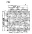
- Fig. 7 shows the structure of the electrodes in the simple matrix panel sealing ferroelectric crystal liquid shown in Fig. 6.
- the example shown in Fig. 7 is a simple matrix panel comprising 4 scanning electrodes 3 and 4 signal electrodes 4, which will be referred to as a 4 x 4 simple matrix panel (the former numeral indicating the number of the scanning electrodes 3 and the latter numeral indicating the number of the signal electrodes 4).
- the scanning electrodes 3 are labeled as L1, L2, L3 and L4 respectively, from the uppermost one, and the signal electrodes are labeled, from the left side, as S1, S2, S3 and S4, respectively.
- the intersection of the scanning electrode L i and the signal electrode S j is represented as a pixel A ij (i and j are positive integer).
- Fig. 8 shows a 16 x 16 simple matrix panel displaying a letter "A".
- Fig. 9 is a diagram of voltage waveforms applied to the scanning electrodes when the panel of Fig. 8 is driven.
- Fig. 10 is a diagram of voltage waveforms applied to the signal electrodes 4 for driving the panel shown in Fig. 8.
- Figs. 11A and 11B are diagrams of voltage waveforms applied to the pixels when the panel shown in Fig. 8 is driven.
- the operation for driving the panel shown in Fig. 8 in accordance with the conventional method of driving will be described in the following.
- the voltage shown in Fig. 9 is applied to the scanning electrode L i by the scanning driver 10, and the voltage shown in Fig. 10 is applied to the signal electrode S j by the signal driver 9.
- the voltages such as shown in Figs. 11A and 11B are applied to the pixel A ij , so that the pixel A ij is set in a bright or dark memory state, thereby displaying the character "A".
- the ferroelectric liquid crystal has two memory states, one of which is referred to as the dark memory state while the other is referred to as the bright memory state.
- the bright memory state and the dark memory state maybe changed with each other.
- the voltage C (the voltage V0, and then the voltage -V0) is applied to the scanning electrodes L1 to L4 as shown in Fig. 9 (a) to (d), while the voltage G (voltage -2V0/3, and then the voltage 2V0/3) is applied to the scanning electrodes L5 to L9 as shown in Fig. 9 (e) to (h).
- the voltage A (voltage -V0 and then voltage V0) is applied to the scanning electrode L1 and the voltage B (voltage 2V0/3 and then the voltage -2V0/3) is applied to the remaining scanning electrodes.
- the voltage A is applied to the scanning electrode L2 and the voltage B is applied to the remaining scanning electrodes.
- the voltage A is applied to the scanning electrode L3 and the voltage B is applied to the remaining scanning electrodes.
- the voltage A is applied to the scanning electrode L4 and the voltage B is applied to the remaining scanning electrodes.
- the voltage C is applied to the scanning electrodes L5 to L8 and the voltage G is applied to the scanning electrode L9 and L1 to L4. Thereafter, the similar operation is repeated.
- the voltage F (voltage -V0 and then voltage V0) is applied to all the signal electrodes S j as shown in Fig. 10.
- the voltage D (voltage V0 and then the voltage -V0) or the voltage E (voltage V0/3 and then voltage -V0/3) is applied to each of the signal electrodes S j .
- the voltage F is applied to all the signal electrodes S j . Thereafter, the same operation is repeated.
- the voltages such as shown in Figs. 11A and 11B are applied to the pixels A ij . More specifically, the voltage applied to the pixel is equal to the voltage applied to the scanning electrode L i minus the voltage applied to the signal electrode S j .
- the voltage shown in Fig. 11A (a) is applied to the pixel A22.
- the voltage CF is applied to the pixels A 1j to A 4j including the pixel A22 during the time period -t0 to 0.
- the voltage 2V0 and then -2V0 are applied to the pixels including the pixel A22, which are set in the dark memory state.
- the ferroelectric liquid crystal sealed in this panel has a nature to be set in the dark memory state when the voltage -2V0 is applied for t0/2.
- the voltage A is supplied to the scanning electrode L2 and the voltage E is applied to the signal electrode S2 during the time period t0 to 2t0, then the voltage AE is applied to the pixel A22, keeping the dark memory state.
- the ferroelectric liquid crystal sealed in this panel has a nature that it is not set to the bright memory state even if the voltage 4V0/3 is applied for t0/2.
- the voltage shown in Fig. 11A (d) is applied to the pixel A 2c . Namely, the voltage CF is applied to the pixels A 1a to A 4j including the pixel A 2c during the time t0 to 0.
- the voltage CF By the voltage CF, the voltage 2V0 and then -2V0 are applied to the pixels including the pixel A 2c , so that these pixels are set to the dark memory state. If the voltage A is applied to the scanning electrode L2 and the voltage D is applied to the signal electrode S c during t0 to 2t0, then the voltage AD is applied, so that the bright memory state is realized.
- the ferroelectric liquid crystal introduced in this panel has a nature that it is set to the bright memory state when the voltage 2V0 is applied for t0/2.
- the pixels A22 and A 2c rewritten in this manner are kept in the bright or dark memory state until the voltage CF is applied the next time as shown in Fig. 11A (a) and (d).
- the erasing voltage C and the non-selection voltage G are applied to a set of scanning electrodes 3, each set including 4 scanning electrodes 3.
- the erasing voltage C and the non-selection voltage G are applied to a set of scanning electrodes 3, each set including 2 to 16 electrodes.
- the scanning time per 1 scanning electrode provided by dividing the above value by the number of scanning electrodes m is about 2.1 x t m (sec).
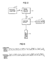
- Fig. 12 is a block diagram for the display of output signal of a conventional personal computer.
- Fig. 13 is a diagram of waveforms showing the output signal of the personal computer and the input signal of the signal driver showing in Fig. 12.
- the scanning time per scanning electrode can be made considerably close to 2t m (sec).
- a timing converting circuit 12 must be provided between the personal computer 11 and the control circuit 13 shown in Fig. 12. The reason for this is that although the output signal from the personal computer 11 is continues to the signal for the scanning electrodes L1, L2, L3, L4, L5, L6 and so on as shown in Fig. 13 (a), the actual signal to be applied to the signal driver 9 must include a signal corresponding to the timing of applying the voltage F to the signal electrode S j as shown in Fig. 13 (b). Therefore, the timing of the output signals of the personal computer 11 must be converted, so that they can be applied to the signal driver 9.
- one object of the present invention is to provide a method of driving a ferroelectric liquid crystal displaying panel in a relatively simple manner without providing a timing converting circuit.
- the liquid crystal displaying panel comprises a plurality of scanning electrodes arranged parallel to each other, signal electrodes arranged parallel to each other intersecting the plurality of scanning electrodes, and ferroelectric liquid crystal sealed between the plurality of scanning electrodes and the plurality of signal electrodes.
- a compensation voltage G is applied followed by a succeeding erasing voltage H to the scanning electrode L i (i is a positive integer) corresponding to a pixel to be displayed out of the plurality of scanning electrodes, and thereafter a selecting voltage A is applied thereto, a bright voltage D is applied to a signal electrode corresponding to the pixel to be displayed, so that the corresponding pixel is turned on.
- the scanning time t0 per scanning electrode can be set twice the pulse width t m necessary for rewriting the memory state of the ferroelectric liquid crystal without providing the timing converting circuit as in the prior art.
- the compensation voltage G is a voltage which becomes negative for a prescribed time period
- the succeeding erasing voltage H is a voltage which becomes positive for a prescribed time period
- the selection voltage A is, in a former half of the predetermined time period, a negative voltage which is approximately equal to the succeeding erasing voltage H and, in the latter half of the period, a positive voltage which is approximately equal to the compensation voltage G
- the bright voltage D is, in the former half of the predetermined period, a positive voltage which is approximately the same as the selection voltage A in the latter half of the period, and in the latter half of the period, it is selected to be a negative voltage which is approximately equal to the selection voltage A in the former half of the period.
- a dark voltage E is applied to the signal electrode corresponding to the pixel to be displayed, so that the corresponding pixel is set in the off state.
- the dark voltage E is selected to be, in the former half of the prescribed period, a positive voltage lower than the bright voltage D in the former half of the period, and in the latter half, it is selected to be a negative voltage higher than the bright voltage D.
- the non-selection voltage B is applied to the scanning electrodes corresponding to the pixels which are not to be displayed, so that these pixels are set to the non-selected state.
- the non-selection voltage B is selected to be, in the former half in the predetermined time period, a positive voltage lower than the selection voltage A in the latter half and higher than the dark voltage E in the former half, and in the latter half of the period, a negative voltage higher than the selection voltage A in the former half and lower than the dark voltage E in the latter half.
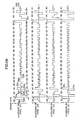
- Fig. 1 is a diagram of waveforms illustrating the principle of the present invention. Referring to Fig. 1, the principle of the present invention will be described. Before the selection voltage A is applied to the scanning electrode L i (i is a positive integer), the compensation voltage G is applied followed by the succeeding erasing voltage H. More specifically, from the time 0 to t0, a selection voltage A having the waveform as shown in Fig. 1 (1), that is, -V a in the former half of a predetermined time period and Va in the latter half of the period, is applied to the scanning electrode L i . A non-selection voltage B having such a waveform as shown in Fig.
- the succeeding erasing voltage H is applied to the scanning electrode L i .
- the voltage -V g - V d is applied in the former half of the period and the voltage -V g + V d is applied in the latter half of the period to the pixel A ij , as shown in Fig. 1 (g). If the dark voltage E shown in Fig.
- the pixel A ij can be kept in the dark memory state, since it is approximately the same as the application of the voltage -V g for the time P x t0 to the pixel A ij no matter whether the bright voltage D is applied or the dark voltage E is applied to the signal electrode S j .
- the compensation voltage G is applied. If the bright voltage D is applied to the signal electrode S j at this time, then, the voltage V g - V d is applied followed by the voltage V g + V d to the pixel A ij as shown in Fig. 1 (e).
- the voltage -V a is applied in the former half and the voltage V a is applied in the latter half as the selection voltage A
- the voltage V b is applied in the former half and the voltage -V b is applied in the latter half as the non-selection voltage B
- the voltage V g is applied as the compensation voltage G and the voltage -V g is applied as the succeeding erasing voltage H
- the voltage V d is applied in the former half and the voltage -V d is applied in the latter half as the bright voltage D
- the voltage V e is applied in the former half and the voltage -V e is applied in the latter half as the dark voltage E.
- the same effect can be obtained provided that the same voltage waveform is applied to the pixel A ij , even if the voltage V z or the like is commonly added to the respective voltages.
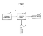
- Fig. 2 is a block diagram showing one embodiment of the present invention.
- a personal computer 11 a control circuit 13 a signal driver 9 and a scanning driver 10.
- the timing converting circuit 12 shown in Fig. 11 is omitted.
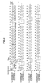
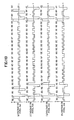
- Fig. 3 is a diagram of voltage waveforms applied to the scanning electrodes when the panel shown in Fig. 8 is driven.
- Fig. 4 is a diagram of voltage waveforms applied to the signal electrodes.
- Figs. 5A and 5B are diagrams of voltage waveforms applied to the pixels.
- a driving method of one embodiment of the present invention will be described in the following.
- the selection voltage A (voltage -V0 and then voltage V0) is applied to the scanning electrode L1; the succeeding erasing voltage H (voltage -V0) is applied to the scanning electrode L2; the compensation voltage G (voltage V0) is applied to the scanning electrode L3; and the non-selection voltage B (voltage 2V0/3 and then voltage -2V0/3) is applied to the scanning electrodes L4 to L9.
- the selection voltage A is applied to the scanning electrode L2
- the succeeding erasing voltage H is applied to the scanning electrode L3
- the compensation voltage G is applied to the scanning electrode L4
- the non-selection voltage B is applied to the scanning electrodes L5 to L9 and to L1.
- the dark voltage E (voltage V0/3 and then voltage -V0/3) or the bright voltage D (voltage V0 and then voltage -V0) is applied to the signal electrode S j .
- the voltages shown in Fig. 4 (a) to (e) are applied to the signal electrodes S2, S6, S b , S c and S d .
- the voltages applied to the pixels A22, A26, A 2b , A 2c , A 2d , A 3b , A32 and A36 are as shown in Fig. 5A (a) to (d) and Fig. 5B (e) to (h).
- the pixel A22 for example, is once set to the dark memory state by the difference voltage between the succeeding erasing voltage H and the dark voltage D or the bright voltage E, that is, HD or HE.
- the sealed ferroelectric liquid crystal is set to the dark memory state by the difference voltage HD as described with reference to the prior art. Approximately the same effect is provided by the difference voltage HE. In view of the variations of the characteristics of the cells, the succeeding erasing voltage H may be applied twice.
- the selection voltage A is applied from the time t0 to 2t0 to the scanning electrode L2.
- the dark voltage E must be applied to the signal electrode S j as shown in Fig. 4 (a) to (c).
- the difference voltage AE is applied to the pixel A 2j as shown in Fig. 5A (a) to (c).
- the memory state of the pixel A 2j is not changed, as shown in the prior art. If the pixel A 2j is to be set to the bright memory state, then the dark voltage D must be applied to the signal electrode S j as shown in Fig. 4 (d) and (e).
- the difference voltage AD is applied to the pixel A 2j as shown in Fig. 5A (d) and Fig. 5B (e) so that the pixel A 2j is changed to the bright memory state.
- a compensation voltage G and then the succeeding erasing voltage H are applied to the scanning electrode L1 before the application of the selection voltage A, so that the scanning time t0 (sec) per each scanning electrode can be set twice the time width t m (sec) of the pulse necessary for rewriting the memory state of the ferroelectric liquid crystal, without providing the timing conversion circuit as in the prior art.
Landscapes
- Engineering & Computer Science (AREA)
- Chemical & Material Sciences (AREA)
- Crystallography & Structural Chemistry (AREA)
- Physics & Mathematics (AREA)
- Computer Hardware Design (AREA)
- General Physics & Mathematics (AREA)
- Theoretical Computer Science (AREA)
- Liquid Crystal Display Device Control (AREA)
- Liquid Crystal (AREA)
- Digital Computer Display Output (AREA)
Applications Claiming Priority (2)
| Application Number | Priority Date | Filing Date | Title |
|---|---|---|---|
| JP63278139A JPH02123327A (ja) | 1988-11-01 | 1988-11-01 | 強誘電性液晶の駆動方法 |
| JP278139/88 | 1988-11-01 |
Publications (3)
| Publication Number | Publication Date |
|---|---|
| EP0367531A2 true EP0367531A2 (fr) | 1990-05-09 |
| EP0367531A3 EP0367531A3 (fr) | 1992-01-22 |
| EP0367531B1 EP0367531B1 (fr) | 1994-12-14 |
Family
ID=17593132
Family Applications (1)
| Application Number | Title | Priority Date | Filing Date |
|---|---|---|---|
| EP89311174A Expired - Lifetime EP0367531B1 (fr) | 1988-11-01 | 1989-10-30 | Méthode de commande d'un panneau d'affichage à cristaux liquides ferro-électriques |
Country Status (4)
| Country | Link |
|---|---|
| US (1) | US5048934A (fr) |
| EP (1) | EP0367531B1 (fr) |
| JP (1) | JPH02123327A (fr) |
| DE (1) | DE68920002T2 (fr) |
Cited By (4)
| Publication number | Priority date | Publication date | Assignee | Title |
|---|---|---|---|---|
| EP0473058A3 (en) * | 1990-08-22 | 1993-04-07 | Canon Kabushiki Kaisha | Liquid crystal apparatus |
| EP0588517A1 (fr) * | 1992-08-25 | 1994-03-23 | Sharp Kabushiki Kaisha | Dispositif de commande pour matrice active et méthode de commande pour matrice active |
| EP0607860A1 (fr) * | 1993-01-13 | 1994-07-27 | Seiko Epson Corporation | Méthode de commande d'un dispositif d'affichage à cristaux liquides |
| US6271817B1 (en) | 1991-03-20 | 2001-08-07 | Seiko Epson Corporation | Method of driving liquid crystal display device that reduces afterimages |
Families Citing this family (4)
| Publication number | Priority date | Publication date | Assignee | Title |
|---|---|---|---|---|
| US5283564A (en) * | 1990-12-26 | 1994-02-01 | Canon Kabushiki Kaisha | Liquid crystal apparatus with temperature-dependent pulse manipulation |
| JP3229156B2 (ja) * | 1995-03-15 | 2001-11-12 | 株式会社東芝 | 液晶表示装置 |
| JP3688574B2 (ja) | 1999-10-08 | 2005-08-31 | シャープ株式会社 | 液晶表示装置および光源装置 |
| JP4076451B2 (ja) | 2003-01-28 | 2008-04-16 | トピー工業株式会社 | 不等厚リム用リム素材、不等厚リム、不等厚リムの製造方法 |
Family Cites Families (13)
| Publication number | Priority date | Publication date | Assignee | Title |
|---|---|---|---|---|
| US4878741A (en) * | 1986-09-10 | 1989-11-07 | Manchester R & D Partnership | Liquid crystal color display and method |
| GB2175725B (en) * | 1985-04-04 | 1989-10-25 | Seikosha Kk | Improvements in or relating to electro-optical display devices |
| JPH0695179B2 (ja) * | 1985-09-06 | 1994-11-24 | 松下電器産業株式会社 | 液晶マトリックス表示パネルの駆動法 |
| SE8504760D0 (sv) * | 1985-10-14 | 1985-10-14 | Sven Torbjorn Lagerwall | Electronic addressing of ferroelectric liquid crystal devices |
| JPS62141520A (ja) * | 1985-12-16 | 1987-06-25 | Casio Comput Co Ltd | 液晶駆動方法 |
| JPH0827601B2 (ja) * | 1986-01-13 | 1996-03-21 | 株式会社日立製作所 | 液晶表示装置、及びその駆動方法 |
| JPS63503285A (ja) * | 1986-05-20 | 1988-12-02 | スマート,ピーター・アイノン | スキー運搬装置 |
| JPS6311912A (ja) * | 1986-07-02 | 1988-01-19 | Mitsubishi Electric Corp | 液晶表示装置の駆動装置 |
| JP2823049B2 (ja) * | 1986-08-13 | 1998-11-11 | キヤノン株式会社 | 二次元表示装置 |
| DE3784809T2 (de) * | 1986-08-18 | 1993-07-08 | Canon Kk | Verfahren und vorrichtung zur ansteuerung einer optischen modulationsanordnung. |
| JPS6373228A (ja) * | 1986-09-17 | 1988-04-02 | Canon Inc | 光学変調素子の駆動法 |
| JP2565925B2 (ja) * | 1987-09-29 | 1996-12-18 | 株式会社東芝 | マトリクス駆動表示装置 |
| US4922240A (en) * | 1987-12-29 | 1990-05-01 | North American Philips Corp. | Thin film active matrix and addressing circuitry therefor |
-
1988
- 1988-11-01 JP JP63278139A patent/JPH02123327A/ja active Pending
-
1989
- 1989-10-25 US US07/426,171 patent/US5048934A/en not_active Expired - Lifetime
- 1989-10-30 EP EP89311174A patent/EP0367531B1/fr not_active Expired - Lifetime
- 1989-10-30 DE DE68920002T patent/DE68920002T2/de not_active Expired - Fee Related
Cited By (7)
| Publication number | Priority date | Publication date | Assignee | Title |
|---|---|---|---|---|
| EP0473058A3 (en) * | 1990-08-22 | 1993-04-07 | Canon Kabushiki Kaisha | Liquid crystal apparatus |
| US5396352A (en) * | 1990-08-22 | 1995-03-07 | Canon Kabushiki Kaisha | Liquid crystal apparatus with gradation information signals and DC bias |
| US5479283A (en) * | 1990-08-22 | 1995-12-26 | Canon Kabushiki Kaisha | Ferroelectric liquid crystal apparatus having a threshold voltage greater than the polarization value divided by the insulating layer capacitance |
| US6271817B1 (en) | 1991-03-20 | 2001-08-07 | Seiko Epson Corporation | Method of driving liquid crystal display device that reduces afterimages |
| EP0588517A1 (fr) * | 1992-08-25 | 1994-03-23 | Sharp Kabushiki Kaisha | Dispositif de commande pour matrice active et méthode de commande pour matrice active |
| US5400048A (en) * | 1992-08-25 | 1995-03-21 | Sharp Kabushiki Kaisha | Active matrix driving apparatus and an active matrix driving method |
| EP0607860A1 (fr) * | 1993-01-13 | 1994-07-27 | Seiko Epson Corporation | Méthode de commande d'un dispositif d'affichage à cristaux liquides |
Also Published As
| Publication number | Publication date |
|---|---|
| US5048934A (en) | 1991-09-17 |
| DE68920002D1 (de) | 1995-01-26 |
| EP0367531A3 (fr) | 1992-01-22 |
| DE68920002T2 (de) | 1995-06-22 |
| EP0367531B1 (fr) | 1994-12-14 |
| JPH02123327A (ja) | 1990-05-10 |
Similar Documents
| Publication | Publication Date | Title |
|---|---|---|
| US5940057A (en) | Method and apparatus for eliminating crosstalk in active matrix liquid crystal displays | |
| EP0391655B1 (fr) | Dispositif de commande d'un appareil d'affichage matriciel à cristaux liquides | |
| EP0651367B1 (fr) | Dispositif pour réduire la consommation d'énergie dans un affichage matriciel basé sur la détection de changements d'image | |
| EP0767449B1 (fr) | Méthode et circuit d'attaque d'un panneau d'affichage à cristaux liquides à matrice active avec contrôle de la tension moyenne de commande | |
| US20110128272A1 (en) | Liquid crystal display accepting alternating common voltage | |
| US6862014B2 (en) | Display driving apparatus and driving control method | |
| US7215310B2 (en) | Liquid crystal display device | |
| AU7424291A (en) | Liquid crystal display apparatus and driving method of such apparatus | |
| US20060119755A1 (en) | Liquid crystal display device | |
| JP2954429B2 (ja) | アクティブマトリクス方式駆動装置 | |
| EP0768557A1 (fr) | Procede et appareil de commande d'un afficheur a cristaux liquides antiferroelectriques | |
| EP0367531B1 (fr) | Méthode de commande d'un panneau d'affichage à cristaux liquides ferro-électriques | |
| JP2007506135A (ja) | 必要メモリを低減された双安定ディスプレイ | |
| EP0770898A1 (fr) | Procede de commande d'affichage a cristaux liquides antiferroelectriques et appareil afferent | |
| EP0503321A1 (fr) | Dispositif d'affichage à cristaux liquides | |
| WO2002101709A1 (fr) | Adressage d'un reseau d'elements d'affichage | |
| JP2003029719A (ja) | 液晶表示装置 | |
| JP2000003158A (ja) | 液晶表示装置 | |
| JP2002072974A (ja) | 液晶駆動装置の駆動方法 | |
| JP3391048B2 (ja) | 液晶装置の駆動方法、液晶装置の駆動回路及び表示装置 | |
| JPH04118625A (ja) | 液晶表示装置の駆動回路 | |
| JPH06149180A (ja) | 液晶表示装置の駆動方法 | |
| MY132482A (en) | Multiplex addressing of ferroelectric liquid crystal displays | |
| EP0492542A2 (fr) | Méthode de commande d'affichage | |
| JPH07210115A (ja) | 液晶駆動装置 |
Legal Events
| Date | Code | Title | Description |
|---|---|---|---|
| PUAI | Public reference made under article 153(3) epc to a published international application that has entered the european phase |
Free format text: ORIGINAL CODE: 0009012 |
|
| AK | Designated contracting states |
Kind code of ref document: A2 Designated state(s): DE FR GB |
|
| 17P | Request for examination filed |
Effective date: 19901214 |
|
| PUAL | Search report despatched |
Free format text: ORIGINAL CODE: 0009013 |
|
| AK | Designated contracting states |
Kind code of ref document: A3 Designated state(s): DE FR GB |
|
| 17Q | First examination report despatched |
Effective date: 19940223 |
|
| GRAA | (expected) grant |
Free format text: ORIGINAL CODE: 0009210 |
|
| AK | Designated contracting states |
Kind code of ref document: B1 Designated state(s): DE FR GB |
|
| REF | Corresponds to: |
Ref document number: 68920002 Country of ref document: DE Date of ref document: 19950126 |
|
| ET | Fr: translation filed | ||
| PLBE | No opposition filed within time limit |
Free format text: ORIGINAL CODE: 0009261 |
|
| STAA | Information on the status of an ep patent application or granted ep patent |
Free format text: STATUS: NO OPPOSITION FILED WITHIN TIME LIMIT |
|
| 26N | No opposition filed | ||
| REG | Reference to a national code |
Ref country code: GB Ref legal event code: IF02 |
|
| PGFP | Annual fee paid to national office [announced via postgrant information from national office to epo] |
Ref country code: FR Payment date: 20041008 Year of fee payment: 16 |
|
| PGFP | Annual fee paid to national office [announced via postgrant information from national office to epo] |
Ref country code: GB Payment date: 20041027 Year of fee payment: 16 |
|
| PGFP | Annual fee paid to national office [announced via postgrant information from national office to epo] |
Ref country code: DE Payment date: 20041028 Year of fee payment: 16 |
|
| PG25 | Lapsed in a contracting state [announced via postgrant information from national office to epo] |
Ref country code: GB Free format text: LAPSE BECAUSE OF NON-PAYMENT OF DUE FEES Effective date: 20051030 |
|
| PG25 | Lapsed in a contracting state [announced via postgrant information from national office to epo] |
Ref country code: DE Free format text: LAPSE BECAUSE OF NON-PAYMENT OF DUE FEES Effective date: 20060503 |
|
| GBPC | Gb: european patent ceased through non-payment of renewal fee |
Effective date: 20051030 |
|
| PG25 | Lapsed in a contracting state [announced via postgrant information from national office to epo] |
Ref country code: FR Free format text: LAPSE BECAUSE OF NON-PAYMENT OF DUE FEES Effective date: 20060630 |
|
| REG | Reference to a national code |
Ref country code: FR Ref legal event code: ST Effective date: 20060630 |