EP0368117A2 - Système d'affichage - Google Patents
Système d'affichage Download PDFInfo
- Publication number
- EP0368117A2 EP0368117A2 EP89120135A EP89120135A EP0368117A2 EP 0368117 A2 EP0368117 A2 EP 0368117A2 EP 89120135 A EP89120135 A EP 89120135A EP 89120135 A EP89120135 A EP 89120135A EP 0368117 A2 EP0368117 A2 EP 0368117A2
- Authority
- EP
- European Patent Office
- Prior art keywords
- information
- display
- scanning
- display information
- write
- Prior art date
- Legal status (The legal status is an assumption and is not a legal conclusion. Google has not performed a legal analysis and makes no representation as to the accuracy of the status listed.)
- Granted
Links
- 230000015654 memory Effects 0.000 claims abstract description 55
- 239000011159 matrix material Substances 0.000 claims abstract description 21
- 239000005262 ferroelectric liquid crystals (FLCs) Substances 0.000 claims description 47
- 230000003446 memory effect Effects 0.000 claims 7
- 230000036961 partial effect Effects 0.000 description 12
- 238000010586 diagram Methods 0.000 description 4
- 230000003247 decreasing effect Effects 0.000 description 3
- 238000012545 processing Methods 0.000 description 3
- 238000000034 method Methods 0.000 description 2
- 230000002829 reductive effect Effects 0.000 description 2
- 239000004990 Smectic liquid crystal Substances 0.000 description 1
- 238000012937 correction Methods 0.000 description 1
- 238000012217 deletion Methods 0.000 description 1
- 230000037430 deletion Effects 0.000 description 1
- 238000001514 detection method Methods 0.000 description 1
- 230000009977 dual effect Effects 0.000 description 1
- 230000006870 function Effects 0.000 description 1
- 230000002401 inhibitory effect Effects 0.000 description 1
- 238000003780 insertion Methods 0.000 description 1
- 230000037431 insertion Effects 0.000 description 1
- 230000002093 peripheral effect Effects 0.000 description 1
- 239000000758 substrate Substances 0.000 description 1
- 230000001360 synchronised effect Effects 0.000 description 1
Images



Classifications
-
- G—PHYSICS
- G09—EDUCATION; CRYPTOGRAPHY; DISPLAY; ADVERTISING; SEALS
- G09G—ARRANGEMENTS OR CIRCUITS FOR CONTROL OF INDICATING DEVICES USING STATIC MEANS TO PRESENT VARIABLE INFORMATION
- G09G3/00—Control arrangements or circuits, of interest only in connection with visual indicators other than cathode-ray tubes
- G09G3/04—Control arrangements or circuits, of interest only in connection with visual indicators other than cathode-ray tubes for presentation of a single character by selection from a plurality of characters, or by composing the character by combination of individual elements, e.g. segments using a combination of such display devices for composing words, rows or the like, in a frame with fixed character positions
- G09G3/16—Control arrangements or circuits, of interest only in connection with visual indicators other than cathode-ray tubes for presentation of a single character by selection from a plurality of characters, or by composing the character by combination of individual elements, e.g. segments using a combination of such display devices for composing words, rows or the like, in a frame with fixed character positions by control of light from an independent source
-
- G—PHYSICS
- G09—EDUCATION; CRYPTOGRAPHY; DISPLAY; ADVERTISING; SEALS
- G09G—ARRANGEMENTS OR CIRCUITS FOR CONTROL OF INDICATING DEVICES USING STATIC MEANS TO PRESENT VARIABLE INFORMATION
- G09G3/00—Control arrangements or circuits, of interest only in connection with visual indicators other than cathode-ray tubes
- G09G3/20—Control arrangements or circuits, of interest only in connection with visual indicators other than cathode-ray tubes for presentation of an assembly of a number of characters, e.g. a page, by composing the assembly by combination of individual elements arranged in a matrix no fixed position being assigned to or needed to be assigned to the individual characters or partial characters
- G09G3/34—Control arrangements or circuits, of interest only in connection with visual indicators other than cathode-ray tubes for presentation of an assembly of a number of characters, e.g. a page, by composing the assembly by combination of individual elements arranged in a matrix no fixed position being assigned to or needed to be assigned to the individual characters or partial characters by control of light from an independent source
- G09G3/36—Control arrangements or circuits, of interest only in connection with visual indicators other than cathode-ray tubes for presentation of an assembly of a number of characters, e.g. a page, by composing the assembly by combination of individual elements arranged in a matrix no fixed position being assigned to or needed to be assigned to the individual characters or partial characters by control of light from an independent source using liquid crystals
- G09G3/3611—Control of matrices with row and column drivers
- G09G3/3622—Control of matrices with row and column drivers using a passive matrix
- G09G3/3629—Control of matrices with row and column drivers using a passive matrix using liquid crystals having memory effects, e.g. ferroelectric liquid crystals
-
- G—PHYSICS
- G09—EDUCATION; CRYPTOGRAPHY; DISPLAY; ADVERTISING; SEALS
- G09G—ARRANGEMENTS OR CIRCUITS FOR CONTROL OF INDICATING DEVICES USING STATIC MEANS TO PRESENT VARIABLE INFORMATION
- G09G2310/00—Command of the display device
- G09G2310/02—Addressing, scanning or driving the display screen or processing steps related thereto
- G09G2310/0224—Details of interlacing
- G09G2310/0227—Details of interlacing related to multiple interlacing, i.e. involving more fields than just one odd field and one even field
-
- G—PHYSICS
- G09—EDUCATION; CRYPTOGRAPHY; DISPLAY; ADVERTISING; SEALS
- G09G—ARRANGEMENTS OR CIRCUITS FOR CONTROL OF INDICATING DEVICES USING STATIC MEANS TO PRESENT VARIABLE INFORMATION
- G09G2310/00—Command of the display device
- G09G2310/04—Partial updating of the display screen
Definitions
- the present invention relates to a display system which realizes an intrawindow smooth scroll display and a cursor/mouse display on a ferroelectric liquid crystal display panel.
- a multiplexing driving scheme for a ferroelectric liquid crystal display panel is disclosed in, e.g., U.S.P. No. 4,655,561 to Kanbe.
- a pulse of one or the other polarity having a peak value and a pulse width enough to satisfactorily cause one or the other of bistable aligning states must be applied at the time of selection of one scanning line. For example, if a selection interval of one scanning line is 150 ⁇ sec, one vertical scanning interval (one frame scanning time) for 400 scanning lines is 60 msec, and a frame frequency is 16.7. When the number of scanning lines is increased, the frame frequency is decreased.
- a smooth shift display of a cursor or mouse can be achieved by a partial updating/scanning scheme for updating and scanning only scanning lines corresponding to a cursor or mouse display portion to be updated.
- Fig. 1 is a block diagram showing a ferroelectric liquid crystal panel control apparatus according to an embodiment of the present invention and its peripheral circuit arrangement.
- the ferroelectric liquid crystal control apparatus includes a drawer 11 such as a CPU, a display information storage memory (VRAM) 12 which can be freely accessed by the drawer 11, a comparator 13 for comparing the data written in the VRAM 12 with the data read out therefrom, and flags 14 which are selectively set when the drawer 11 writes data in the VRAM 12.
- the number of flags corresponds to the number of display lines on the FLC (ferroelectric liquid crystal) panel.
- the ferroelectric liquid crystal control apparatus also includes a sequencer 15 for generating a display address or checking and resetting the flags 13, and an FCL panel 16 for performing a display.
- the read modify write function of the memory is used to read out data and then compare whether or not the readout data is identical with the write data. If the readout data is identical with the write data, the drawer 11 then writes the data at a designated address of the VRAM 12. However, when these data are not identical, the flag 14 corresponding to this address is set.
- a normal dynamic RAM can simultaneously perform write access and read access, a dual port RAM frequently used as a display memory requires a longer processing time, as shown in a timing chart of Fig. 2.
- each flag 14 can be a one-bit flag for a one-line address of the memory.
- the sequencer 15 normally performs interlaced display refreshing and checks the flags 14. If all the flags 14 corresponding to the respective lines are not set, refreshing must be repeated. However, if some flags 14 are set, the addresses of the VRAM 12 are calculated by the number of these set flags. The sequencer 15 sends corresponding one-line data to the FLC panel 16, and the set flags 14 are cleared.
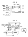
- Fig. 3 shows a relationship between the VRAM 12 and the flags 14 when the FLC panel 16 of 640 x 400 dots is used. Note that an address and data are represented as xxH (hexadecimal notation). For example, 01H is “01" in hexadecimal notation, and 4FH is "4F" in hexadecimal notation.
- this range corresponds to display data of the first line.
- the first one of the flags 14 is set. Furthermore, when the first flag is already set, data of 00H to 4FH is transferred to the FLC panel 16 as the first-line data. In a normal operation, when all the flags 14 are not refreshed, the sequencer 15 performs interlaced display refreshing. If some flags 14 are set upon checking of all the flags, addresses of the VRAM 12 are calculated as described above, and the corresponding data are transferred to the FLC panel 16. The set flags 14 corresponding to the display lines are reset.
- partial updating can be detected by a 400-bit memory serving as the flags 14.
- a one-bit flag for two or four lines may be used to send four-line data to the FLC panel 16 if only of the dots of the four lines is updated.
- the memory capacity for the flags 14 can be further decreased.
- 20 lines are used as one row and the above-mentioned panel of 640 x 400 dots is used as a display for displaying 20 rows, updating can be performed in units of rows.
- a 20-bit memory can be added to constitute the flags 14 so as to detect partial updating.
- Fig. 4 shows a display system according to another embodiment using a timer 41 for determining a minimum refresh scanning frequency.
- Fig. 5 is a flow chart for explaining the operation of the display system shown in Fig. 4.
- step S10 the sequencer 15 transfers display data (one-field data) of the VRAM 12 to the FLC panel 16.
- the flags 14 corresponding to the transferred display line data are cleared.
- step S11 after one-field data is transferred, the sequencer 15 checks all the flags 14.
- step S12 when all the flags 14 are reset, the sequencer 15 resets the timer 41, and the flow returns to step S10. As described above, refreshing of the FLC panel 16 is repeated.
- step S11 the sequencer 15 checks all the flags 14. If the sequencer 15 determines in step S12 that the flag 14 corresponding to a given display line is set, the display data of the given display line of the flag 14 is transferred to the FLC panel 16. The flag 14 corresponding to the given display line is cleared.
- step S14 the sequencer 15 checks a count time of the timer 41. In step S15, when the count time of the timer 41 does not exceed a predetermined value, the flow returns to step S11, and the sequencer 15 checks the flags 14 again.
- step S15 When the count time of the timer exceeds the predetermined value in step S15, the timer is cleared to zero in step S16, and the flow returns to step S10 again.
- step S15 determines in step S15 whether a predetermined period of time has elapsed. If YES in step S15, the sequencer 15 interrupts partial updating/scanning and resets the timer 41. Refreshing of the sequencer 15 is then restored. When the sequencer 15 checks the flags 14 upon refreshing of one field, the remaining flags 14 are kept set, and the remaining write operations continue.
- Fig. 6 shows a display system using a flag counter 61 for counting ON flags of flags 14 according to still another embodiment of the present invention.
- a sequencer 15 In a normal operation, when all the flags 14 are reset, a sequencer 15 generates addresses for interlaced display refreshing and transfers display data (one-field data) from a VRAM 12 to an FLC panel 16. The flag 14 corresponding to the transferred display line data is cleared. After one-field data is transferred, the sequencer 15 counts the number of ON flags of the flags 14 in step S11. In step S12, the sequencer 15 uses the flag counter 61 to count the number of ON flags 14. When write access of the VRAM 12 is completed by the drawer 11, the flags 14 of the display lines corresponding to the addresses are set.
- step S12 If the number n of ON flags 14 is 0 or a predetermined value m or more, e.g., 1/4 or more of all the display lines, in step S12, the flow returns from step S12 to step S10, and refreshing of the FLC panel 16 is repeated.
- the sequencer 15 counts the number n of ON flags 14 in step S11.
- step S12 the count of the flag counter 61 is checked by the sequencer 15. If the number of ON flags falls within the range of 0 ⁇ n ⁇ m, the display data of display lines corresponding to the ON flags are transferred to the FLC panel 16 in step S13. The flow returns to step S10, and refreshing is repeated.
- Fig. 8 is a timing chart of scanning line address information A and an image signal B output from the VRAM 12 to the FCL panel 16.
- a one-horizontal scanning interval corresponds to one scan selection interval.
- the horizontal sync signal HD is set at high level, the scanning line address information A is detected.
- the horizontal sync signal HD is set at low level, the image signal B is detected.
- the horizontal sync signal HD is synchronous with an indication signal.
- a scheme for applying a scan selection signal to scanning lines corresponding to only a partial updating area can be applied to a partial updating scheme used in the present invention, as disclosed in U.S.P. Nos. 4,655,561 and 4,693,563.
- This partial updating scheme is not limited to a character correction display within the display screen, but can also be utilized for a multiwindow display, an intrawindow scroll display, and a cursor or mouse shift display designated from a pointing device.
- Fig. 9 shows a multiwindow screen display.
- the multiwindow display screen consists of different layers in different display areas.
- Window 1 represents a layer for expressing a summation result in a circle graph.
- Window 2 represents a layer for expressing the summation result of window 1 in a table.
- Window 3 represents a layer expressing the summation result of window 1 in a bar graph.
- Window 4 represents a layer associated with documentation.
- the background is white.
- window 4 is a work layer and other windows are kept in a still image state. That is, window 4 is kept in a dynamic display state during documentation.
- Detailed operations in the dynamic state are scrolling, insertion, deletion, and copying of words and clauses, and a block shift. These operations require relatively high-speed processing. Display operations will be exemplified below.
- a character font has a 16 x 16 dot format.
- 16 scanning lines are updated. Therefore, these 16 scanning lines are scanned and driven.
- window 4 is set in a smooth scroll state.
- the number of scanning lines constituting window 4 is 400.
- a smooth scroll display is performed by scanning and driving only these 400 scanning lines, thereby updating these lines.
- a scan selection signal is cyclically applied.
- a one-screen content must be obtained by one-frame scanning (or one-field scanning) (in other words, it is necessary to complete selective write access of a one-scanning line black pixel display based on a dark state of the FLC and a one-scanning line white pixel display based on a bright state of the FLC during each scanning of one scanning line).
- the refreshing/scanning scheme used in the present invention is preferably a "multi-interlaced scanning scheme" for selectively applying a scan selection singal every two or more scanning lines, and more preferably every four or more scanning lines (the selection signal is preferably applied every four to 20 scanning lines).
- Fig. 10A shows a scan selection signal S S , a scan nonselection signal S N , a white information signal I W , and a black information signal I B .
- Fig. 10B shows a waveform of a voltage applied to a selected pixel (this pixel is applied with the white information signal I W and a voltage (I W - S S )) of pixels (intersections between the scanning electrodes and the information electrodes) on the scan selection electrodes applied with the scan selection signal S S , a waveform of a voltage applied to a nonselected pixel (this pixel is applied with the black information signal I B and a voltage (I B - S S )) on the same scan selection electrode, and a waveform of a voltage applied to two types of pixels on scan nonselection electrodes applied with the scan nonselection signal.
- a voltage (-(V1 + V3) serving as a voltage exceeding one FLC threshold voltage is applied to the nonselected pixel on the scan selection electrode at a phase t1.
- One aligning state of the FLC is caused to obtain a dark state, thereby completing black write access.
- a voltage (-V1 + V3) serving as a voltage lower than the above FLC threshold value is applied to the selected pixel on the scan selection electrode, thereby inhibiting a change in aligning state.
- a voltage (V2 + V3) serving as a voltage exceeding the other FLC threshold value is applied to the selected pixel on the scan selection electrode, so that the FLC is changed to the other aligning state to obtain a bright state, thereby writing a white pixel.
- a voltage (V2 - V3) serving as a voltage below the other FLC threshold value is applied to the nonselected pixel on the scan selection electrode.
- the previous aligning state at the phase t1 is not changed.
- Voltages ⁇ V3 below the FLC threshold values are applied to the pixels on the scan nonselection electrodes at the phases t1 and t2. For this reason, in this embodiment, white or black data is written in the pixel on the scan electrode selected at a phase T1. Even if a scan nonselection signal is then applied to this pixel, the write state is maintained.
- a voltage having a polarity opposite to the information signal obtained at the write phase T1 is applied from the information electrode at a phase T2. Therefore, as shown in Fig. 10C, an AC voltage is applied to the pixel during scan nonselection, thereby improving the FLC threshold characteristics.
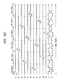
- Fig. 10C is a timing chart of voltage waveforms for obtaining a certain display state.
- the scan selection signal is applied every five scanning electrodes so that the scan selection signals are applied to scanning electrodes which are not adjacent to each other.
- the scanning electrodes are selected every five electrodes, and one-frame scanning is completed by six field scanning cycles.
- a scan selection period (T1 + T2) is set to be long at a low temperature, and flickering can be greatly suppressed even in scanning at a low frame frequency (e.g., a frame frequency of 5 to 10 Hz).
- scan selection signals are applied to scanning electrodes which are not adjacent to each other during scanning of six fields, and picture torn can be effectively prevented.
- An FLC element used in the present invention can be selected from ones disclosed in U.S.P. Nos. 4,367,924, 4,639,089, 4,655,561, 4,697,887, and 4,712,873.
- a cell thickness i.e., a distance between upper and lower substrates
- a cell thickness is set to be small enough to suppress occurrence of a spiral aligning state inherent to a chiral smectic layer in a bulk state, thereby obtaining a bistable aligning state.
- write access of the display memory by the drawer is simultaneously performed with its read access, and therefore, the processing time can be shortened.
- a flag representing a comparison result may have one bit for one display line
- the flags can be constituted by a memory having the number of bits corresponding to the number of display lines. Therefore, partial write access can be detected by adding a memory having a capacity of a fraction of several millions of the total capacity as compared with a method using two display memories.
- the present invention can be achieved by only easy hardware from which the capacity of the display memory can be reduced, thereby advantageously using a large volume of software.
- flags representing that partial write access was completed are provided in correspondence with the display lines of the FLC display. Partial write access can be detected by adding a memory having a capacity of a fraction of several millions of the total capacity as compared with a method using two display memories.
- the present invention can be achieved by only easy hardware from which the capacity of the display memory can be reduced, thereby advantageously using a large volume of software.
- the flags corresponding to the display lines which have been updated in correspondence with any display lines in the display memory during partial updating are set, and only the partially updated display data can be transferred with reference to the set flags. Therefore, even during scanning at a low frame frequency, a cursor position designated by a pointing device can be shifted and displayed at high speed.
- multi-interlaced scanning refreshing of the FLC display is performed every predetermined period, thereby suppressing picture disturbance such as a decrease in contrast level at a position on the screen where no flickering occurs and partial write access is not performed.
- a cursor display can be optimized.
- a display system comprises:
Landscapes
- Engineering & Computer Science (AREA)
- Physics & Mathematics (AREA)
- Computer Hardware Design (AREA)
- General Physics & Mathematics (AREA)
- Theoretical Computer Science (AREA)
- Chemical & Material Sciences (AREA)
- Crystallography & Structural Chemistry (AREA)
- Liquid Crystal Display Device Control (AREA)
- Selective Calling Equipment (AREA)
- Alarm Systems (AREA)
- Input Circuits Of Receivers And Coupling Of Receivers And Audio Equipment (AREA)
- Control Of Indicators Other Than Cathode Ray Tubes (AREA)
Applications Claiming Priority (8)
| Application Number | Priority Date | Filing Date | Title |
|---|---|---|---|
| JP273181/88 | 1988-10-31 | ||
| JP63273181A JP2652220B2 (ja) | 1988-10-31 | 1988-10-31 | 強誘電性液晶表示装置および表示制御装置 |
| JP27317988A JP2577623B2 (ja) | 1988-10-31 | 1988-10-31 | 強誘電性液晶制御装置 |
| JP273182/88 | 1988-10-31 | ||
| JP273180/88 | 1988-10-31 | ||
| JP63273182A JP2652221B2 (ja) | 1988-10-31 | 1988-10-31 | 強誘電性液晶表示装置および表示制御装置 |
| JP27318088A JP2617345B2 (ja) | 1988-10-31 | 1988-10-31 | 強誘電性液晶制御装置 |
| JP273179/88 | 1988-10-31 |
Publications (3)
| Publication Number | Publication Date |
|---|---|
| EP0368117A2 true EP0368117A2 (fr) | 1990-05-16 |
| EP0368117A3 EP0368117A3 (fr) | 1991-10-30 |
| EP0368117B1 EP0368117B1 (fr) | 1996-04-10 |
Family
ID=27478988
Family Applications (1)
| Application Number | Title | Priority Date | Filing Date |
|---|---|---|---|
| EP89120135A Expired - Lifetime EP0368117B1 (fr) | 1988-10-31 | 1989-10-30 | Système d'affichage |
Country Status (8)
| Country | Link |
|---|---|
| US (2) | US5760790A (fr) |
| EP (1) | EP0368117B1 (fr) |
| KR (1) | KR940003426B1 (fr) |
| AT (1) | ATE136676T1 (fr) |
| AU (1) | AU634725B2 (fr) |
| DE (1) | DE68926212T2 (fr) |
| ES (1) | ES2088386T3 (fr) |
| GR (1) | GR3019964T3 (fr) |
Cited By (23)
| Publication number | Priority date | Publication date | Assignee | Title |
|---|---|---|---|---|
| EP0435701A3 (en) * | 1989-12-29 | 1992-08-26 | Sharp Kabushiki Kaisha | Display control method and apparatus for ferroelectric liquid crystal panel |
| EP0464620A3 (en) * | 1990-06-27 | 1992-12-23 | Canon Kabushiki Kaisha | Image information control apparatus and display system |
| EP0478381A3 (en) * | 1990-09-27 | 1993-03-24 | Sharp Kabushiki Kaisha | Display control method and apparatus for liquid crystal display device |
| EP0533473A1 (fr) * | 1991-09-18 | 1993-03-24 | Canon Kabushiki Kaisha | Dispositif de contrôle d'affichage |
| EP0541366A1 (fr) * | 1991-11-08 | 1993-05-12 | Canon Kabushiki Kaisha | Dispositif de commande d'affichage |
| EP0525786A3 (en) * | 1991-08-02 | 1993-05-19 | Canon Kabushiki Kaisha | Display control apparatus |
| EP0537428A3 (en) * | 1991-08-02 | 1993-07-28 | Canon Kabushiki Kaisha | Display control apparatus |
| EP0558342A1 (fr) * | 1992-02-28 | 1993-09-01 | Canon Kabushiki Kaisha | Système et méthode de contrôle d'une unité d'affichage |
| EP0570906A1 (fr) * | 1992-05-19 | 1993-11-24 | Canon Kabushiki Kaisha | Méthode et dispositif de commande d'affichage |
| EP0572143A1 (fr) * | 1992-05-19 | 1993-12-01 | Canon Kabushiki Kaisha | Méthode et dispositif de commande d'affichage |
| EP0591683A1 (fr) * | 1992-09-04 | 1994-04-13 | Canon Kabushiki Kaisha | Dispositif et méthode de commande d'affichage |
| EP0592801A1 (fr) * | 1992-09-04 | 1994-04-20 | Canon Kabushiki Kaisha | Dispositif et méthode de commande d'affichage |
| EP0591682A3 (en) * | 1992-09-04 | 1994-06-29 | Canon Kk | Display control apparatus |
| US5357267A (en) * | 1990-06-27 | 1994-10-18 | Canon Kabushiki Kaisha | Image information control apparatus and display system |
| EP0581594A3 (fr) * | 1992-07-31 | 1995-01-04 | Canon Kk | Dispositif de commande d'affichage. |
| US5576738A (en) * | 1993-09-24 | 1996-11-19 | International Business Machines Corporation | Display apparatus with means for detecting changes in input video |
| US5596345A (en) * | 1992-04-17 | 1997-01-21 | International Business Machines Corporation | Method for managing non-rectangular windows in a raster display |
| US5699075A (en) * | 1992-01-31 | 1997-12-16 | Canon Kabushiki Kaisha | Display driving apparatus and information processing system |
| US5844532A (en) * | 1993-01-11 | 1998-12-01 | Canon Inc. | Color display system |
| US5926159A (en) * | 1992-05-19 | 1999-07-20 | Canon Kabushiki Kaisha | Display control apparatus and method therefor capable of limiting an area for partial rewriting |
| US6088806A (en) * | 1998-10-20 | 2000-07-11 | Seiko Epson Corporation | Apparatus and method with improved power-down mode |
| US6097388A (en) * | 1995-08-22 | 2000-08-01 | International Business Machines Corporation | Method for managing non-rectangular windows in a raster display |
| US6097364A (en) * | 1992-07-29 | 2000-08-01 | Canon Kabushiki Kaisha | Display control apparatus which compresses image data to reduce the size of a display memory |
Families Citing this family (7)
| Publication number | Priority date | Publication date | Assignee | Title |
|---|---|---|---|---|
| JP3280306B2 (ja) | 1998-04-28 | 2002-05-13 | インターナショナル・ビジネス・マシーンズ・コーポレーション | 画像情報送信方法、画像情報更新方法、送信装置及び更新装置 |
| US20020143618A1 (en) * | 2001-03-29 | 2002-10-03 | Kenner Martin A. | Payment based content recipient access to software notes posted at content provider site |
| US20020143900A1 (en) * | 2001-03-29 | 2002-10-03 | Kenner Martin A. | Content recipient access to software notes posted at content provider site |
| US7343415B2 (en) * | 2001-03-29 | 2008-03-11 | 3M Innovative Properties Company | Display of software notes indicating that content from a content provider site is available for display |
| KR100922796B1 (ko) * | 2003-02-05 | 2009-10-21 | 엘지디스플레이 주식회사 | 액정표시장치의 데이터 로딩방법 및 장치 |
| KR100568539B1 (ko) * | 2004-01-30 | 2006-04-07 | 삼성전자주식회사 | 디스플레이 데이터 제어회로, 이 회로를 위한 메모리, 및이 메모리의 어드레스 발생방법 |
| KR101028584B1 (ko) | 2008-08-27 | 2011-04-12 | 주식회사 바이오프로테크 | 일회용 유도전극 및 이에 접속되는 리드선 |
Citations (3)
| Publication number | Priority date | Publication date | Assignee | Title |
|---|---|---|---|---|
| US4655561A (en) | 1983-04-19 | 1987-04-07 | Canon Kabushiki Kaisha | Method of driving optical modulation device using ferroelectric liquid crystal |
| US4693563A (en) | 1984-07-05 | 1987-09-15 | Seiko Instruments & Electronics Ltd. | Ferro-electric liquid crystal electro-optical device |
| EP0237742A2 (fr) | 1986-02-07 | 1987-09-23 | BMC Software, Inc. | Prétraitement d'entrée pour un système télématique |
Family Cites Families (15)
| Publication number | Priority date | Publication date | Assignee | Title |
|---|---|---|---|---|
| US4367924A (en) * | 1980-01-08 | 1983-01-11 | Clark Noel A | Chiral smectic C or H liquid crystal electro-optical device |
| US4331977A (en) * | 1980-12-15 | 1982-05-25 | Zenith Radio Corporation | Portable television controller with electronic switching |
| JPS5853268A (ja) * | 1981-09-25 | 1983-03-29 | Nippon Telegr & Teleph Corp <Ntt> | フアクシミリの回線制御方式 |
| JPS60156043A (ja) * | 1984-01-23 | 1985-08-16 | Canon Inc | カイラルスメクティック液晶素子 |
| JPS60220316A (ja) * | 1984-04-16 | 1985-11-05 | Canon Inc | 液晶光学素子 |
| US4697887A (en) * | 1984-04-28 | 1987-10-06 | Canon Kabushiki Kaisha | Liquid crystal device and method for driving the same using ferroelectric liquid crystal and FET's |
| JPS6159265A (ja) * | 1984-08-31 | 1986-03-26 | Soaa:Kk | 図形表示用液晶表示装置 |
| US4691200A (en) * | 1984-10-01 | 1987-09-01 | Xerox Corporation | Matrix display with a fast cursor |
| JPS6184989A (ja) * | 1984-10-02 | 1986-04-30 | Sony Corp | タイマ−装置 |
| JPS61272724A (ja) * | 1985-05-27 | 1986-12-03 | Seiko Epson Corp | 液晶表示装置 |
| US4796203A (en) * | 1986-08-26 | 1989-01-03 | Kabushiki Kaisha Toshiba | High resolution monitor interface and related interfacing method |
| US5264839A (en) * | 1987-09-25 | 1993-11-23 | Canon Kabushiki Kaisha | Display apparatus |
| CA1319767C (fr) * | 1987-11-26 | 1993-06-29 | Canon Kabushiki Kaisha | Afficheur |
| EP0416172B1 (fr) * | 1989-09-08 | 1996-07-24 | Canon Kabushiki Kaisha | Système de traitement d'informations avec panneau d'affichage |
| US5357267A (en) * | 1990-06-27 | 1994-10-18 | Canon Kabushiki Kaisha | Image information control apparatus and display system |
-
1989
- 1989-10-27 AU AU43885/89A patent/AU634725B2/en not_active Ceased
- 1989-10-30 ES ES89120135T patent/ES2088386T3/es not_active Expired - Lifetime
- 1989-10-30 DE DE68926212T patent/DE68926212T2/de not_active Expired - Fee Related
- 1989-10-30 AT AT89120135T patent/ATE136676T1/de not_active IP Right Cessation
- 1989-10-30 EP EP89120135A patent/EP0368117B1/fr not_active Expired - Lifetime
- 1989-10-31 KR KR1019890015719A patent/KR940003426B1/ko not_active Expired - Fee Related
-
1994
- 1994-03-24 US US08/217,133 patent/US5760790A/en not_active Expired - Fee Related
-
1995
- 1995-05-01 US US08/432,007 patent/US5629717A/en not_active Expired - Fee Related
-
1996
- 1996-05-20 GR GR960401338T patent/GR3019964T3/el unknown
Patent Citations (3)
| Publication number | Priority date | Publication date | Assignee | Title |
|---|---|---|---|---|
| US4655561A (en) | 1983-04-19 | 1987-04-07 | Canon Kabushiki Kaisha | Method of driving optical modulation device using ferroelectric liquid crystal |
| US4693563A (en) | 1984-07-05 | 1987-09-15 | Seiko Instruments & Electronics Ltd. | Ferro-electric liquid crystal electro-optical device |
| EP0237742A2 (fr) | 1986-02-07 | 1987-09-23 | BMC Software, Inc. | Prétraitement d'entrée pour un système télématique |
Cited By (37)
| Publication number | Priority date | Publication date | Assignee | Title |
|---|---|---|---|---|
| EP0435701A3 (en) * | 1989-12-29 | 1992-08-26 | Sharp Kabushiki Kaisha | Display control method and apparatus for ferroelectric liquid crystal panel |
| US5357267A (en) * | 1990-06-27 | 1994-10-18 | Canon Kabushiki Kaisha | Image information control apparatus and display system |
| EP0464620A3 (en) * | 1990-06-27 | 1992-12-23 | Canon Kabushiki Kaisha | Image information control apparatus and display system |
| US5726675A (en) * | 1990-06-27 | 1998-03-10 | Canon Kabushiki Kaisha | Image information control apparatus and display system |
| EP0478381A3 (en) * | 1990-09-27 | 1993-03-24 | Sharp Kabushiki Kaisha | Display control method and apparatus for liquid crystal display device |
| US5289173A (en) * | 1990-09-27 | 1994-02-22 | Sharp Kabushiki Kaisha | Display control method having partial rewriting operation |
| US5644332A (en) * | 1991-08-02 | 1997-07-01 | Canon Kabushiki Kaisha | Apparatus and method for controlling drive of a display device in accordance with the number of scanning lines to be updated |
| EP0525786A3 (en) * | 1991-08-02 | 1993-05-19 | Canon Kabushiki Kaisha | Display control apparatus |
| EP0537428A3 (en) * | 1991-08-02 | 1993-07-28 | Canon Kabushiki Kaisha | Display control apparatus |
| US5686934A (en) * | 1991-08-02 | 1997-11-11 | Canon Kabushiki Kaisha | Display control apparatus |
| EP0533473A1 (fr) * | 1991-09-18 | 1993-03-24 | Canon Kabushiki Kaisha | Dispositif de contrôle d'affichage |
| US5977945A (en) * | 1991-09-18 | 1999-11-02 | Canon Kabushiki Kaisha | Display control apparatus |
| EP0541366A1 (fr) * | 1991-11-08 | 1993-05-12 | Canon Kabushiki Kaisha | Dispositif de commande d'affichage |
| US5481274A (en) * | 1991-11-08 | 1996-01-02 | Canon Kabushiki Kaisha | Display control device |
| US5699075A (en) * | 1992-01-31 | 1997-12-16 | Canon Kabushiki Kaisha | Display driving apparatus and information processing system |
| US5717420A (en) * | 1992-02-28 | 1998-02-10 | Canon Kabushiki Kaisha | Display control apparatus and method |
| EP0558342A1 (fr) * | 1992-02-28 | 1993-09-01 | Canon Kabushiki Kaisha | Système et méthode de contrôle d'une unité d'affichage |
| US5596345A (en) * | 1992-04-17 | 1997-01-21 | International Business Machines Corporation | Method for managing non-rectangular windows in a raster display |
| EP0570906A1 (fr) * | 1992-05-19 | 1993-11-24 | Canon Kabushiki Kaisha | Méthode et dispositif de commande d'affichage |
| US5926159A (en) * | 1992-05-19 | 1999-07-20 | Canon Kabushiki Kaisha | Display control apparatus and method therefor capable of limiting an area for partial rewriting |
| US5613103A (en) * | 1992-05-19 | 1997-03-18 | Canon Kabushiki Kaisha | Display control system and method for controlling data based on supply of data |
| EP0572143A1 (fr) * | 1992-05-19 | 1993-12-01 | Canon Kabushiki Kaisha | Méthode et dispositif de commande d'affichage |
| US5379051A (en) | 1992-05-19 | 1995-01-03 | Canon Kabushiki Kaisha | Method and apparatus for rearranging and displaying line data |
| US6097364A (en) * | 1992-07-29 | 2000-08-01 | Canon Kabushiki Kaisha | Display control apparatus which compresses image data to reduce the size of a display memory |
| EP0581594A3 (fr) * | 1992-07-31 | 1995-01-04 | Canon Kk | Dispositif de commande d'affichage. |
| US6091389A (en) * | 1992-07-31 | 2000-07-18 | Canon Kabushiki Kaisha | Display controlling apparatus |
| EP0591682A3 (en) * | 1992-09-04 | 1994-06-29 | Canon Kk | Display control apparatus |
| EP0592801A1 (fr) * | 1992-09-04 | 1994-04-20 | Canon Kabushiki Kaisha | Dispositif et méthode de commande d'affichage |
| EP0591683A1 (fr) * | 1992-09-04 | 1994-04-13 | Canon Kabushiki Kaisha | Dispositif et méthode de commande d'affichage |
| US5736981A (en) * | 1992-09-04 | 1998-04-07 | Canon Kabushiki Kaisha | Display control apparatus |
| US6157359A (en) * | 1992-09-04 | 2000-12-05 | Canon Kabushiki Kaisha | Display control apparatus |
| US6075508A (en) * | 1992-09-04 | 2000-06-13 | Canon Kabushiki Kaisha | Display control apparatus and method therefor |
| US6140996A (en) * | 1992-09-04 | 2000-10-31 | Canon Kabushiki Kaisha | Display control apparatus |
| US5844532A (en) * | 1993-01-11 | 1998-12-01 | Canon Inc. | Color display system |
| US5576738A (en) * | 1993-09-24 | 1996-11-19 | International Business Machines Corporation | Display apparatus with means for detecting changes in input video |
| US6097388A (en) * | 1995-08-22 | 2000-08-01 | International Business Machines Corporation | Method for managing non-rectangular windows in a raster display |
| US6088806A (en) * | 1998-10-20 | 2000-07-11 | Seiko Epson Corporation | Apparatus and method with improved power-down mode |
Also Published As
| Publication number | Publication date |
|---|---|
| AU634725B2 (en) | 1993-03-04 |
| EP0368117B1 (fr) | 1996-04-10 |
| DE68926212T2 (de) | 1996-10-02 |
| GR3019964T3 (en) | 1996-08-31 |
| ES2088386T3 (es) | 1996-08-16 |
| KR940003426B1 (ko) | 1994-04-22 |
| DE68926212D1 (de) | 1996-05-15 |
| US5629717A (en) | 1997-05-13 |
| US5760790A (en) | 1998-06-02 |
| EP0368117A3 (fr) | 1991-10-30 |
| AU4388589A (en) | 1990-05-03 |
| KR900006903A (ko) | 1990-05-09 |
| ATE136676T1 (de) | 1996-04-15 |
Similar Documents
| Publication | Publication Date | Title |
|---|---|---|
| US5760790A (en) | Display system | |
| US5321419A (en) | Display apparatus having both refresh-scan and partial-scan | |
| US5583534A (en) | Method and apparatus for driving liquid crystal display having memory effect | |
| US5606343A (en) | Display device | |
| US6320562B1 (en) | Liquid crystal display device | |
| EP0533472B1 (fr) | Appareil de commande d'affichage | |
| US5894297A (en) | Display apparatus | |
| KR860001450B1 (ko) | 그래픽 디스플레이 시스템 | |
| US5896118A (en) | Display system | |
| US5905483A (en) | Display control apparatus | |
| EP0494605B1 (fr) | Dispositif à cristaux liquides | |
| EP0592801B1 (fr) | Dispositif et méthode de commande d'affichage | |
| JP2652221B2 (ja) | 強誘電性液晶表示装置および表示制御装置 | |
| JP2652220B2 (ja) | 強誘電性液晶表示装置および表示制御装置 | |
| JPH08241060A (ja) | 液晶表示装置及びその駆動方法 | |
| JP2577623B2 (ja) | 強誘電性液晶制御装置 | |
| JP2617345B2 (ja) | 強誘電性液晶制御装置 | |
| JP3227200B2 (ja) | 表示制御装置及び方法 | |
| JPH08248388A (ja) | 液晶表示装置 | |
| JP2003186454A (ja) | 平面表示装置 | |
| JP3483291B2 (ja) | 液晶素子の駆動方法および駆動装置ならびにそれらを用いた表示装置 | |
| JP2002182616A (ja) | 液晶表示装置 | |
| JPH05224628A (ja) | 表示パネルの駆動法 | |
| JPS63172194A (ja) | マトリクス表示装置 |
Legal Events
| Date | Code | Title | Description |
|---|---|---|---|
| PUAI | Public reference made under article 153(3) epc to a published international application that has entered the european phase |
Free format text: ORIGINAL CODE: 0009012 |
|
| AK | Designated contracting states |
Kind code of ref document: A2 Designated state(s): AT BE CH DE ES FR GB GR IT LI LU NL SE |
|
| 17P | Request for examination filed |
Effective date: 19901221 |
|
| PUAL | Search report despatched |
Free format text: ORIGINAL CODE: 0009013 |
|
| AK | Designated contracting states |
Kind code of ref document: A3 Designated state(s): AT BE CH DE ES FR GB GR IT LI LU NL SE |
|
| 17Q | First examination report despatched |
Effective date: 19931019 |
|
| GRAA | (expected) grant |
Free format text: ORIGINAL CODE: 0009210 |
|
| AK | Designated contracting states |
Kind code of ref document: B1 Designated state(s): AT BE CH DE ES FR GB GR IT LI LU NL SE |
|
| REF | Corresponds to: |
Ref document number: 136676 Country of ref document: AT Date of ref document: 19960415 Kind code of ref document: T |
|
| REF | Corresponds to: |
Ref document number: 68926212 Country of ref document: DE Date of ref document: 19960515 |
|
| ET | Fr: translation filed | ||
| ITF | It: translation for a ep patent filed | ||
| REG | Reference to a national code |
Ref country code: ES Ref legal event code: BA2A Ref document number: 2088386 Country of ref document: ES Kind code of ref document: T3 |
|
| REG | Reference to a national code |
Ref country code: CH Ref legal event code: NV Representative=s name: BOVARD AG PATENTANWAELTE Ref country code: GR Ref legal event code: FG4A Free format text: 3019964 |
|
| GRAH | Despatch of communication of intention to grant a patent |
Free format text: ORIGINAL CODE: EPIDOS IGRA |
|
| REG | Reference to a national code |
Ref country code: ES Ref legal event code: FG2A Ref document number: 2088386 Country of ref document: ES Kind code of ref document: T3 |
|
| PLBE | No opposition filed within time limit |
Free format text: ORIGINAL CODE: 0009261 |
|
| STAA | Information on the status of an ep patent application or granted ep patent |
Free format text: STATUS: NO OPPOSITION FILED WITHIN TIME LIMIT |
|
| 26N | No opposition filed | ||
| REG | Reference to a national code |
Ref country code: GB Ref legal event code: IF02 |
|
| PGFP | Annual fee paid to national office [announced via postgrant information from national office to epo] |
Ref country code: SE Payment date: 20021004 Year of fee payment: 14 |
|
| PGFP | Annual fee paid to national office [announced via postgrant information from national office to epo] |
Ref country code: FR Payment date: 20021008 Year of fee payment: 14 |
|
| PGFP | Annual fee paid to national office [announced via postgrant information from national office to epo] |
Ref country code: AT Payment date: 20021011 Year of fee payment: 14 |
|
| PGFP | Annual fee paid to national office [announced via postgrant information from national office to epo] |
Ref country code: GR Payment date: 20021024 Year of fee payment: 14 |
|
| PGFP | Annual fee paid to national office [announced via postgrant information from national office to epo] |
Ref country code: LU Payment date: 20021029 Year of fee payment: 14 |
|
| PGFP | Annual fee paid to national office [announced via postgrant information from national office to epo] |
Ref country code: GB Payment date: 20021030 Year of fee payment: 14 |
|
| PGFP | Annual fee paid to national office [announced via postgrant information from national office to epo] |
Ref country code: NL Payment date: 20021031 Year of fee payment: 14 Ref country code: ES Payment date: 20021031 Year of fee payment: 14 Ref country code: DE Payment date: 20021031 Year of fee payment: 14 |
|
| PGFP | Annual fee paid to national office [announced via postgrant information from national office to epo] |
Ref country code: CH Payment date: 20021101 Year of fee payment: 14 |
|
| PGFP | Annual fee paid to national office [announced via postgrant information from national office to epo] |
Ref country code: BE Payment date: 20021219 Year of fee payment: 14 |
|
| PG25 | Lapsed in a contracting state [announced via postgrant information from national office to epo] |
Ref country code: LU Free format text: LAPSE BECAUSE OF NON-PAYMENT OF DUE FEES Effective date: 20031030 Ref country code: GB Free format text: LAPSE BECAUSE OF NON-PAYMENT OF DUE FEES Effective date: 20031030 Ref country code: AT Free format text: LAPSE BECAUSE OF NON-PAYMENT OF DUE FEES Effective date: 20031030 |
|
| PG25 | Lapsed in a contracting state [announced via postgrant information from national office to epo] |
Ref country code: SE Free format text: LAPSE BECAUSE OF NON-PAYMENT OF DUE FEES Effective date: 20031031 Ref country code: LI Free format text: LAPSE BECAUSE OF NON-PAYMENT OF DUE FEES Effective date: 20031031 Ref country code: ES Free format text: LAPSE BECAUSE OF NON-PAYMENT OF DUE FEES Effective date: 20031031 Ref country code: CH Free format text: LAPSE BECAUSE OF NON-PAYMENT OF DUE FEES Effective date: 20031031 Ref country code: BE Free format text: LAPSE BECAUSE OF NON-PAYMENT OF DUE FEES Effective date: 20031031 |
|
| BERE | Be: lapsed |
Owner name: *CANON K.K. Effective date: 20031031 |
|
| PG25 | Lapsed in a contracting state [announced via postgrant information from national office to epo] |
Ref country code: NL Free format text: LAPSE BECAUSE OF NON-PAYMENT OF DUE FEES Effective date: 20040501 Ref country code: DE Free format text: LAPSE BECAUSE OF NON-PAYMENT OF DUE FEES Effective date: 20040501 |
|
| PG25 | Lapsed in a contracting state [announced via postgrant information from national office to epo] |
Ref country code: GR Free format text: LAPSE BECAUSE OF NON-PAYMENT OF DUE FEES Effective date: 20040504 |
|
| EUG | Se: european patent has lapsed | ||
| REG | Reference to a national code |
Ref country code: CH Ref legal event code: PL |
|
| GBPC | Gb: european patent ceased through non-payment of renewal fee |
Effective date: 20031030 |
|
| PG25 | Lapsed in a contracting state [announced via postgrant information from national office to epo] |
Ref country code: FR Free format text: LAPSE BECAUSE OF NON-PAYMENT OF DUE FEES Effective date: 20040630 |
|
| NLV4 | Nl: lapsed or anulled due to non-payment of the annual fee |
Effective date: 20040501 |
|
| REG | Reference to a national code |
Ref country code: FR Ref legal event code: ST |
|
| REG | Reference to a national code |
Ref country code: ES Ref legal event code: FD2A Effective date: 20031031 |
|
| PG25 | Lapsed in a contracting state [announced via postgrant information from national office to epo] |
Ref country code: IT Free format text: LAPSE BECAUSE OF NON-PAYMENT OF DUE FEES;WARNING: LAPSES OF ITALIAN PATENTS WITH EFFECTIVE DATE BEFORE 2007 MAY HAVE OCCURRED AT ANY TIME BEFORE 2007. THE CORRECT EFFECTIVE DATE MAY BE DIFFERENT FROM THE ONE RECORDED. Effective date: 20051030 |