EP0368588A2 - Détecteur pyroélectrique et infrarouge et son procédé de fabrication - Google Patents
Détecteur pyroélectrique et infrarouge et son procédé de fabrication Download PDFInfo
- Publication number
- EP0368588A2 EP0368588A2 EP89311464A EP89311464A EP0368588A2 EP 0368588 A2 EP0368588 A2 EP 0368588A2 EP 89311464 A EP89311464 A EP 89311464A EP 89311464 A EP89311464 A EP 89311464A EP 0368588 A2 EP0368588 A2 EP 0368588A2
- Authority
- EP
- European Patent Office
- Prior art keywords
- pyroelectric
- pyroelectric element
- element array
- slit
- elements
- Prior art date
- Legal status (The legal status is an assumption and is not a legal conclusion. Google has not performed a legal analysis and makes no representation as to the accuracy of the status listed.)
- Granted
Links
Images

Classifications
-
- G—PHYSICS
- G08—SIGNALLING
- G08B—SIGNALLING SYSTEMS, e.g. PERSONAL CALLING SYSTEMS; ORDER TELEGRAPHS; ALARM SYSTEMS
- G08B13/00—Burglar, theft or intruder alarms
- G08B13/18—Actuation by interference with heat, light, or radiation of shorter wavelength; Actuation by intruding sources of heat, light, or radiation of shorter wavelength
- G08B13/189—Actuation by interference with heat, light, or radiation of shorter wavelength; Actuation by intruding sources of heat, light, or radiation of shorter wavelength using passive radiation detection systems
- G08B13/19—Actuation by interference with heat, light, or radiation of shorter wavelength; Actuation by intruding sources of heat, light, or radiation of shorter wavelength using passive radiation detection systems using infrared-radiation detection systems
- G08B13/191—Actuation by interference with heat, light, or radiation of shorter wavelength; Actuation by intruding sources of heat, light, or radiation of shorter wavelength using passive radiation detection systems using infrared-radiation detection systems using pyroelectric sensor means
Definitions
- the present invention relates to a device for detecting a location of an object using a pyroelectric infrared sensor.
- a device for detecting a location of an infrared source using an infrared sensor has come into use of late years for the purpose of prevention of crimes and calamities such as detection of an invader and a fire and the like.
- an infrared sensor there are a quantum type using a compound semiconductor and a thermal type using a pyroelectric element or a thermister, etc. Since it is required for the quantum type infrared sensor to be cooled by liquid nitrogen and the like, the thermal type infrared sensor is used for the purpose of prevention of crimes and calamities and the like.
- the pyroelectric sensor has a higher sensitivity than other thermal type sensors, and is therefore optimum for a position detector for a source of infrared radiation.
- a pyroelectric sensor detects a temperature change of a sensor due to the variation of receiving quantity of infrared radiation as a voltage variation. Therefore, such a method in which infrared radiation interrupted by a rotating optical chopper and the like is irradiated to an arranged pyroelectric sensor array and outputs of respective sensors are compared after impedance conversion and a.c. amplification of outputs of these sensors, thereby to detect a position of a source of infrared radiation, is being employed.
- the number of arranged pyroelectric elements is increased.
- the number of processing circuits for impedance conversion and a.c. amplification and the like for the pyroelectric elements is increased accordingly.
- the number of wirings between respective pyroelectric elements and processing circuits is also increased, thereby causing distribution of wirings to become complicated.
- the number of elements and the number of processing circuits are increased in proportion to the square of the resolution, and wiring between pyroelectric elements and processing circuits becomes difficult.
- the device becomes large in size and the production cost thereof is also increased at the same time in a conventional example.
- pyroelectric element array arranged at least in one row or more and a slit interrupting an infrared image which is incident to the pyroelectric element array, respective pyroelectric elements forming one row of said pyroelectric element array are wired so that they are connected in series electrically and adjacent pyroelectric elements generate counter-electromotive forces and said slit is moved in a row direction on said pyroelectric element array, thereby to scan the infrared image which is being irradiated on respective pyroelectric elements in succession, thus obtaining an infrared image irradiated on respective pyroelectric elements from time series signals produced at both ends of said pyroelectric element array.
- pyroelectric element array is scanned optically in succession, outputs of respective pyroelectric elements may be obtained easily as time series signals, and loading into a microprocessor and the like is made easily.
- a pyroelectric infrared sensor always requires an optical chopper as shown in the conventional example.
- the device serves both as an optical chopper and a means for scanning the pyroelectric element array. Therefore, it is not required to add a special mechanism and the device does not become large in size even if a slit is provided.
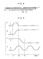
- Fig. 1 shows a plan view, a cross-sectional view and an equivalent circuit showing an embodiment of a pyroelectric infrared detector according to the present invention.
- Electrodes 2 and 3 are formed on both sides of a pyroelectric thin film 1, thus forming pyroelectric elements.
- adjacent elements (next element to each other) of respective pyroelectric elements in a lateral direction are connected alternately by the pattern of electrodes 2 and 3, and pyroelectric elements arranged in one row are connected in series.
- a plurality of rows of said pyroelectric element array are arranged in a longitudinal direction, thus forming a pyroelectric element array in two dimensions.
- an infrared image 5 incident to the pyroelectric element array is scanned, and a voltage generated between electrode 6 and 7 across both ends of each row is applied as an output to a signal processing circuit.
- a signal of a certain pyroelectric element 8 is observed, it is comprehended that other pyroelectric elements are equivalent to those capacitors that are connected in series. Accordingly, the voltage generated at the pyroelectric element 8 becomes equal to the output signal when a signal processing circuit having a sufficiently high input impedance is connected. In other words, the output voltage is the sum of outputs of respective pyroelectric elements.
- the quantity of infrared radiation irradiated on a certain pyroelectric element 20 is varied in accordance with the movement of the slit as shown at a.
- the variation of the output voltage of the pyroelectric element 20 is in proportion to the temperature change of the element, and the temperature change of the element is in proportion to the absorbed quantity of the infrared radiation. Therefore, when it is assumed that the loss of quantity of heat due to thermal diffusion and the like is sufficiently small, the output voltage is in proportion to an integral value of the quantity of irradiated infrared radiation and shows a waveform as shown at b.
- an adjacent pyroelectroc element 21 is connected with a polarity reverse to the pyroelectric element 20, the element 21 has a polarity reverse to that of the pyroelectric element 20, and is delayed in time, showing a waveform shown at c.
- a voltage produced at an output terminal is obtained by obtaining output waveforms of other respective pyroelectric elements in a similar manner as above and adding them up, which shows a waveform as shown at d.
- the overlap with the signal of the adjacent pyroelectric element becomes large and respective signals can not be handled as independent signals individually unless the slit width is made at a cycle period of the pyroelectric element or less.
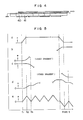
- Fig. 4 and Fig. 5 show an example of the slit other than the above.
- a slit which is wider than the horizontal direction of the pyroelectric element array is used, and Fig. 4 shows a state that infrared radiation has started to be irradiated to a pyroelectric element 40.
- the elapsed variation of the quantity of infrared radiation irradiated to the pyroelectric element 40 is shown at a, and the output voltage thereof is shown at b.
- An output voltage of a next pyroelectric element 41 is shown at c.
- signals of respective pyroelectric elements may be obtained by devicing the shape of the slit and the processing method.
- pyroelectric elements are connected in series. Therefore, the whole electrostatic capacity becomes smaller as the number of elements increases, and the signal voltage is lowered unless the input impedance of the signal processing circuit is made high. Since a thin film is used in the pyroelectric body in the present embodiment, the capacity of each pyroelectric element is large, which is advantageous in point of abovementioned problems. Moreover, there is a material (PbLaTiO3 group) in which polarization axes are made uniform simultaneously with film formation in the material for a pyroelectric thin film, and it is not required to apply polarization process for making polarization of the whole pyroelectric elements uniform by using the above-mentioned material, thus making the manufacture easy.
- a material PbLaTiO3 group
- a pyroelectric infrared detector which has a high performance of positional resolution and in which wiring of a pyroelectric element array and processing circuits is simple, the number of processing circuits is small thus making the size compact, and processing of positional information may be performed easily with a microprocessor.
Landscapes
- Physics & Mathematics (AREA)
- General Physics & Mathematics (AREA)
- Photometry And Measurement Of Optical Pulse Characteristics (AREA)
- Radiation Pyrometers (AREA)
Applications Claiming Priority (2)
| Application Number | Priority Date | Filing Date | Title |
|---|---|---|---|
| JP63280792A JPH0726868B2 (ja) | 1988-11-07 | 1988-11-07 | 焦電型赤外線検知装置とその駆動方法 |
| JP280792/88 | 1988-11-07 |
Publications (3)
| Publication Number | Publication Date |
|---|---|
| EP0368588A2 true EP0368588A2 (fr) | 1990-05-16 |
| EP0368588A3 EP0368588A3 (fr) | 1991-03-06 |
| EP0368588B1 EP0368588B1 (fr) | 1995-05-10 |
Family
ID=17630026
Family Applications (1)
| Application Number | Title | Priority Date | Filing Date |
|---|---|---|---|
| EP89311464A Expired - Lifetime EP0368588B1 (fr) | 1988-11-07 | 1989-11-06 | Détecteur pyroélectrique et infrarouge et son procédé de fabrication |
Country Status (4)
| Country | Link |
|---|---|
| US (1) | US5021660A (fr) |
| EP (1) | EP0368588B1 (fr) |
| JP (1) | JPH0726868B2 (fr) |
| DE (1) | DE68922580T2 (fr) |
Cited By (1)
| Publication number | Priority date | Publication date | Assignee | Title |
|---|---|---|---|---|
| CN102589717A (zh) * | 2010-12-24 | 2012-07-18 | 精工爱普生株式会社 | 检测装置、传感器设备以及电子设备 |
Families Citing this family (8)
| Publication number | Priority date | Publication date | Assignee | Title |
|---|---|---|---|---|
| US5159200A (en) * | 1991-04-12 | 1992-10-27 | Walter Kidde Aerospace Inc. | Detector for sensing hot spots and fires in a region |
| CA2118597C (fr) * | 1991-11-04 | 2001-12-11 | Paul W. Kruse, Jr. | Reseau d'imagerie pyroelectrique en couches minces |
| US5283551A (en) * | 1991-12-31 | 1994-02-01 | Aritech Corporation | Intrusion alarm system |
| JP2002131127A (ja) * | 2000-10-25 | 2002-05-09 | Matsushita Electric Works Ltd | 焦電素子の感度測定装置及び方法 |
| US6712668B2 (en) * | 2000-12-06 | 2004-03-30 | Therma Corporation, Inc. | System and method for electropolishing nonuniform pipes |
| US20110169859A1 (en) * | 2005-04-22 | 2011-07-14 | Lu-Cheng Chen | Portable information product |
| US7498576B2 (en) * | 2005-12-12 | 2009-03-03 | Suren Systems, Ltd. | Temperature detecting system and method |
| US8766187B2 (en) * | 2010-10-25 | 2014-07-01 | Nec Tokin Corporation | Pyroelectric sensor array and pyroelectric infrared detection device |
Family Cites Families (6)
| Publication number | Priority date | Publication date | Assignee | Title |
|---|---|---|---|---|
| SU469061A1 (ru) * | 1973-05-23 | 1975-04-30 | Институт Физики Ан Ссср | Пироэлектрический приемник излучени |
| US3842276A (en) * | 1973-06-15 | 1974-10-15 | Rca Corp | Thermal radiation detector |
| US4072863A (en) * | 1976-10-26 | 1978-02-07 | Roundy Carlos B | Pyroelectric infrared detection system |
| JPS57175930A (en) * | 1981-04-24 | 1982-10-29 | Matsushita Electric Ind Co Ltd | Pyroelectric type linear array light detector |
| JPS57203926A (en) * | 1981-06-09 | 1982-12-14 | Matsushita Electric Ind Co Ltd | Pyro-electric type infrared detection device |
| JPS5935118A (ja) * | 1982-08-24 | 1984-02-25 | Matsushita Electric Ind Co Ltd | 熱赤外線検知装置 |
-
1988
- 1988-11-07 JP JP63280792A patent/JPH0726868B2/ja not_active Expired - Fee Related
-
1989
- 1989-11-03 US US07/431,176 patent/US5021660A/en not_active Expired - Lifetime
- 1989-11-06 DE DE68922580T patent/DE68922580T2/de not_active Expired - Fee Related
- 1989-11-06 EP EP89311464A patent/EP0368588B1/fr not_active Expired - Lifetime
Cited By (1)
| Publication number | Priority date | Publication date | Assignee | Title |
|---|---|---|---|---|
| CN102589717A (zh) * | 2010-12-24 | 2012-07-18 | 精工爱普生株式会社 | 检测装置、传感器设备以及电子设备 |
Also Published As
| Publication number | Publication date |
|---|---|
| JPH03251728A (ja) | 1991-11-11 |
| US5021660A (en) | 1991-06-04 |
| EP0368588A3 (fr) | 1991-03-06 |
| JPH0726868B2 (ja) | 1995-03-29 |
| DE68922580T2 (de) | 1996-01-18 |
| DE68922580D1 (de) | 1995-06-14 |
| EP0368588B1 (fr) | 1995-05-10 |
Similar Documents
| Publication | Publication Date | Title |
|---|---|---|
| US5567942A (en) | Infrared array sensor system | |
| US4614938A (en) | Dual channel pyroelectric intrusion detector | |
| EP0368588B1 (fr) | Détecteur pyroélectrique et infrarouge et son procédé de fabrication | |
| JPH0682305A (ja) | 2次元検出器 | |
| US4596930A (en) | Arrangement for multispectal imaging of objects, preferably targets | |
| US4779005A (en) | Multiple detector viewing of pixels using parallel time delay and integration circuitry | |
| US4873442A (en) | Method and apparatus for scanning thermal images | |
| JPH0868860A (ja) | X線画像センサ | |
| JP2002044371A (ja) | 複数の検出装置を使用した高速スキャナ | |
| US4737642A (en) | Arrangement for multispectral imaging of objects, preferably targets | |
| JPH0341305A (ja) | 焦電型赤外線検知装置 | |
| JP2689644B2 (ja) | 焦電型赤外線検知装置 | |
| JP2590763B2 (ja) | 赤外線固体撮像素子 | |
| JP2523948B2 (ja) | 焦電型赤外線検知装置 | |
| JP2000230858A (ja) | 撮像素子 | |
| JPH09318442A (ja) | 赤外線検出装置 | |
| JPS61173124A (ja) | 焦電型熱画像装置 | |
| JPH0321888A (ja) | 焦電型赤外線検知装置 | |
| JP2000019013A (ja) | 赤外線検出装置 | |
| EP0281172A1 (fr) | Appareil de conversion opto-électrique | |
| JP2728116B2 (ja) | 撮像装置 | |
| JP3023157B2 (ja) | 太陽センサの光入射位置検出装置 | |
| JP2819620B2 (ja) | イメージセンサの駆動装置 | |
| JPH02248820A (ja) | 焦電型赤外線検知装置 | |
| JPS6166112A (ja) | 移動物体の移動姿勢検出装置 |
Legal Events
| Date | Code | Title | Description |
|---|---|---|---|
| PUAI | Public reference made under article 153(3) epc to a published international application that has entered the european phase |
Free format text: ORIGINAL CODE: 0009012 |
|
| AK | Designated contracting states |
Kind code of ref document: A2 Designated state(s): DE FR GB |
|
| PUAL | Search report despatched |
Free format text: ORIGINAL CODE: 0009013 |
|
| 17P | Request for examination filed |
Effective date: 19901228 |
|
| AK | Designated contracting states |
Kind code of ref document: A3 Designated state(s): DE FR GB |
|
| 17Q | First examination report despatched |
Effective date: 19930707 |
|
| GRAA | (expected) grant |
Free format text: ORIGINAL CODE: 0009210 |
|
| AK | Designated contracting states |
Kind code of ref document: B1 Designated state(s): DE FR GB |
|
| REF | Corresponds to: |
Ref document number: 68922580 Country of ref document: DE Date of ref document: 19950614 |
|
| ET | Fr: translation filed | ||
| PLBE | No opposition filed within time limit |
Free format text: ORIGINAL CODE: 0009261 |
|
| STAA | Information on the status of an ep patent application or granted ep patent |
Free format text: STATUS: NO OPPOSITION FILED WITHIN TIME LIMIT |
|
| 26N | No opposition filed | ||
| REG | Reference to a national code |
Ref country code: GB Ref legal event code: 746 Effective date: 19970901 |
|
| REG | Reference to a national code |
Ref country code: GB Ref legal event code: IF02 |
|
| PGFP | Annual fee paid to national office [announced via postgrant information from national office to epo] |
Ref country code: GB Payment date: 20051102 Year of fee payment: 17 |
|
| PGFP | Annual fee paid to national office [announced via postgrant information from national office to epo] |
Ref country code: DE Payment date: 20051103 Year of fee payment: 17 |
|
| PGFP | Annual fee paid to national office [announced via postgrant information from national office to epo] |
Ref country code: FR Payment date: 20051108 Year of fee payment: 17 |
|
| PG25 | Lapsed in a contracting state [announced via postgrant information from national office to epo] |
Ref country code: DE Free format text: LAPSE BECAUSE OF NON-PAYMENT OF DUE FEES Effective date: 20070601 |
|
| GBPC | Gb: european patent ceased through non-payment of renewal fee |
Effective date: 20061106 |
|
| REG | Reference to a national code |
Ref country code: FR Ref legal event code: ST Effective date: 20070731 |
|
| PG25 | Lapsed in a contracting state [announced via postgrant information from national office to epo] |
Ref country code: GB Free format text: LAPSE BECAUSE OF NON-PAYMENT OF DUE FEES Effective date: 20061106 |
|
| PG25 | Lapsed in a contracting state [announced via postgrant information from national office to epo] |
Ref country code: FR Free format text: LAPSE BECAUSE OF NON-PAYMENT OF DUE FEES Effective date: 20061130 |