EP0368655B1 - Übertragungssystem mit einem gemeinsamen Speicher - Google Patents
Übertragungssystem mit einem gemeinsamen Speicher Download PDFInfo
- Publication number
- EP0368655B1 EP0368655B1 EP89311594A EP89311594A EP0368655B1 EP 0368655 B1 EP0368655 B1 EP 0368655B1 EP 89311594 A EP89311594 A EP 89311594A EP 89311594 A EP89311594 A EP 89311594A EP 0368655 B1 EP0368655 B1 EP 0368655B1
- Authority
- EP
- European Patent Office
- Prior art keywords
- data
- register
- common memory
- address
- interruption signal
- Prior art date
- Legal status (The legal status is an assumption and is not a legal conclusion. Google has not performed a legal analysis and makes no representation as to the accuracy of the status listed.)
- Expired - Lifetime
Links
Images




Classifications
-
- G—PHYSICS
- G06—COMPUTING OR CALCULATING; COUNTING
- G06F—ELECTRIC DIGITAL DATA PROCESSING
- G06F15/00—Digital computers in general; Data processing equipment in general
- G06F15/16—Combinations of two or more digital computers each having at least an arithmetic unit, a program unit and a register, e.g. for a simultaneous processing of several programs
- G06F15/163—Interprocessor communication
- G06F15/167—Interprocessor communication using a common memory, e.g. mailbox
Definitions
- the present invention relates to a system for communicating between data processing systems and between units constituting a data processing system.
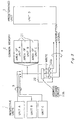
- FIG. 1 shows a prior art communication system using a common memory.
- a writable and readable memory is co-owned by a plurality of units (for example, unit A and unit B) 1 and a special meaning (for example, a command area or data area) is given to the predetermined address of the common memory 2.
- unit A1 When unit A1 intends to send something to unit B1, predetermined data such as commands are written in a predetermined address of the common memory in unit A1.
- Unit B1 enables the data to be read out periodically from the previously defined address by using a well known polling method and recognizes the above communication data transmitted from unit A1.
- unit B1 According to the communication system of the above prior art method, it is necessary for unit B1 to periodically perform a polling to common memory 2.
- the communication speed depends on the polling period of unit B1 and therefore cannot reach the desired level.
- EP-A-0 304 880 which is cited in accordance with A. 54(3) and (4) EPC, discloses a communication system in which sets of mailboxes are used to exchange messages between modules, each source module being able to access its mailbox in the recipient module and to thereupon interrupt said recipient module.
- EP-A-0 201 020 discloses a communication system according to the preamble of accompanying claim 1.
- a flip-flop stores the status of a mailbox for each unit, so that the need for polling is reduced and each unit can easily determine the status of sent messages.
- a communication system in which a common memory is used by a plurality of units, said common memory having a plurality of areas corresponding to respective said units, and said communication system comprising:
- the present invention can thus provide a communication system in which the communication speed in a common memory is not limited by the polling period of the common memory when, in a communication between data process systems or between units constituting a data process system, polling is conducted by the unit on the receiving side.
- an interruption signal 4 is transmitted from a unit (A) 1 to a unit (B) 1 in accordance with a writing 3 to a predetermined address of the common memory 2, the predetermined address in the common memory corresponding to unit (A).
- Unit (B) 1 receives an interruption signal 4 produced by unit 22. It performs an interruption process and reads the data in a predetermined area of the common memory 2, the predetermined area corresponding to the interruption signal, thereby performing a communication between units.
- the present invention provides a communication system between data processing systems and between units constituting a data process system.
- a predetermined unit for example unit (B)
- a writing 3 corresponding to the event is conducted in the predetermined address of the common memory from the unit (A) and the address of the common memory is decoded by an address decoder 22, it produces an interruption signal 4 to a predetermined unit (B).
- the predetermined unit (B) receiving the interruption signal 4 reads the predetermined address corresponding to the kind of interruption signal 4 to recognize the content of the event.
- a predetermined event can be notified quickly from one unit (A) to another (B) and thus, the unit receiving the notification does not need to apply a polling process to the common memory 2. Therefore, the structure of a common control program of a unit (A, B) is simplified, thereby increasing the processing capability of respective units (A, B).
- FIG. 3 shows a block diagram of an embodiment of the present invention.
- a unit 22 decodes the address in which the data is written as shown by a writing 3 in the common memory 2 from respective units (communication units A, B, C...) 1 and produces an interruption signal 4 to the predetermined unit (D) 1.
- This unit 22 is important in realizing the present invention.
- the same reference numbers show the same items throughout all the drawings.
- the present embodiment does not relate to two-way communication but to one-way communication in which the data is transmitted from units (A, B, and C) to notify a certain event to unit (D).
- units (A, B, and C) to notify a certain event to unit (D).
- Unit (D) 1 reads the content of areas 21 of the common memory 2 (namely, the areas corresponding to units (A), (B) and (C)) which are previously determined in accordance with three kinds of interruption signals 4, thereby quickly recognizing the above notification event.
- the present invention provides a system for communicating between data processing systems and between units forming a data processing system. It writes, as shown by a writing 3, a code of an event in an address corresponding to the units (A, B, and C) on the common memory 2 when the event occurring in respective units (A, B, and C) is notified to the other unit (D). Then it produces an interruption signal 4 for the other unit by decoding the writing address in common memory 2, and notifies the other unit (D) of the occurrence of the event by using different interruption signals 4.
- the present communication system performs a communication between data processing systems and units constituting a data processing system.
- a unit produces an interruption signal 4 to a predetermined unit (D) by using a writing 3 into a predetermined address of the common memory, the address corresponding to respective units (A, B and C).
- the interruption signal 4 produced by unit 22 is received through the interruption process for unit (D) 1 to read predetermined area data of the common memory in accordance with the interruption signal 4, thereby performing a communication between units.
- a predetermined event can be notified from one unit to another at high speed and the unit receiving the notification does not need to perform a polling process to the common memory 2. This simplifies the structure of the control program in respective units (A, B, C, D...) 1 and includes a processing capability of respective units.
- FIG. 4 A detailed circuit of a memory access controller (MAC) 30 of a communication system using the common memory in accordance with the present invention is shown in Figure 4.
- MAC memory access controller
- Processors (1), (2), (3)....(8) 31 are connected to common memory 32, through system information bus (SIBUS) 33 which is used as a common bus.
- SIBUS system information bus
- Another processor corresponds to unit D of Figure 3 and comprises a service processor (SVP) 34.
- SVP service processor
- the embodiment shown in Figure 4 comprises 8 processors (1)...(8) 31 and SVP 34 which communicates with them, thereby providing a communication control system using a common memory 32, in which N vs. 1 communication is conducted.
- MAC 30 further comprises system information bus input registers (SIBIR (0), (1) and (2)) 35 and multiplexer (MPX), first command register (CMD) 36, first address register (ADR) 37 and first write data register (WDR) 38, decoder 39 and memory control logic circuit (MEM CNTL) 40, first read data register (RDR) 41, second read data register (RDR) 42, interruption register (INTR) 43, second command register (CMD) 44, second address register (ADR) 45, second write data register (WDR) 46 and system information bus output register (SIBOR) 47.
- the outputs of respective information bus input registers (SIBIR (0), (1) and (2)) 35 are connected to multiplexer (MPX).
- the output of the multiplexer (MPX) is connected to first command register (CMD) 36, first address register (ADR) 37 and first write data register (WDR) 38.
- the output of first command register (CMD) 36 and first address register (ADR) 37 are connected to decoder 39 and the output of first write data register 38 is connected to common memory 32.
- the output of first address register 37 is also connected to a gate (G) to provide the address signal for common memory 32.
- the data read from common memory 32 is set in first read data register (RDR) 41 and the output of first read data register 41 is provided to second read data register (RDR) 42.
- An interruption signal obtained by decoding the output from first command register (CMD) 36 and first address register (ADR) 37 by decoder 39 is set in interruption register (INTR) 43.
- System information buffer in register (SIBIR(0), (1) and (2)) 35 is formed to have three kinds of information set therein so that the differences in time between 4-bit-command, 18-bit-address and 16-bit-writing data is absorbed.
- Multiplexer (MPX) selects the above three kinds of information. The selected information is set in respective registers 36, 37 and 38 after they are divided into 4-bit-command, 18-bit-address and 16-bit write data.
- Decoder 39 decodes the outputs of first command register 36 and first address register 37 as recited above.
- First command register (CMD) 36 receives a write command and first address register 37 receives a particular address, thereby forming an 8-bit interruption signal.
- the 8-bit interruption signal corresponds to the request for the interruption received from processors (1)...(8) 31 and the thus-obtained interruption signal is set in interruption register (INTR) 43.
- memory controller (MEM CNTL) 40 performs a write control of common memory 32 by obtaining write data from first write register (WDR) 38 and stores the 16-bit write data in an address designated by first address register (ADR) 37.
- the storing areas correspond to respective processors (1)...(8) and the write data is stored in an area corresponding to the processor which requests an interruption operation.
- the interruption signal from the decoder 39 is set in interruption register 43 and is provided to service processor 34 as an interruption request signal.
- Service processor (SVP) 34 receives the interruption signal and determines which of bits 0 to 7 in interruption register 43 is 1 and enables an interruption process routine so that the communication areas of the common memory 32 corresponding to processors 1 to 8 are read. Therefore, service processor (SVP) 34 performs a read and write operation for common memory 32. Therefore, the 4-bit read command outputted from service processor (SVP) 34 is stored in the second command register (CMD) 44.
- This 4-bit command (CMD) is provided to memory controller (MEM CNTL) 40 through first command (CMD) register 36 to perform a read operation of common memory 32.
- the reading address is provided by service processor (SVP) 34 as 18 bit address data through second address register (ADR) 45.
- the read out content is provided to service processor (SVP) 34 through first and second read registers (RDR) 41 and 42.
- the write command is set in second command register (CMD) 44 and the write data is set in second write register (WDR) 46, thereby controlling memory controller (MEM CNTL) 40 to perform a write operation for common memory 32 by writing the write data into common memory 32.
- FIG. 5 shows a flowchart of an interruption process routine applied to common memory 32 and is conducted by the service processor (SVP) 34.
- SVP service processor
- ST1 interruption register
- ST2 interruption register
- ST3 processor number among the processors (1) to (8) depending on which of bits 0 to 7 is 1.
- the processor (1) When the processor (1) sends an interruption request to common memory 32, it stores the data in the area corresponding to the processor (1) in the common memory and the service processor (SVP) 34 executes a read operation for the communication area in common memory 32 (ST4), the communication area corresponding to the processor (1). Therefore, the service processor (SVP) 34 sets a read command and read address in the second command register (CMD) and the second address register (ADR) 45, respectively, to read common memory 32 and the content of common memory 32 is read out to service processor (SVP) 34.
- CMD command register
- ADR second address register
- step ST5 the process analyzes the command which is provided as a part of data obtained from the communication area of common memory 32, thereby transmitting the data as a message transmission to a task of the service processor (SVP) 34 in accordance with the command (ST6).
- the service processor (SVP) 34 has a plurality of kinds of tasks corresponding to respective processes, and the data is transmitted to the respective tasks based on the result of the analysis of the command in accordance with data transmitted by the corresponding processor. Therefore, generally speaking, N vs. 1 communication is possible between processors (1) to (8) and service processor (SVP) 34.
- FIG. 6 shows a detailed diagram of the communication system using the common memory in a case of N vs. N processors.
- the same reference numbers as shown in Figure 4 represent the same items.
- the embodiment shown in Figure 6 differs from the embodiment shown in Figure 4, which represents the N vs. 1 communication case, as follows.
- the output of decoder 39 namely, the interruption request signal of 8 bits is set in an interruption register (INTR) 43.
- the content of interruption register (INTR) 43 is sent to the service processor (SVP) 34, which is different from processors (1) to (8).
- the service processor (SVP) 34 is not used and the interruption signal is again transmitted to processors (1) to (8).
- the interruption register (INTR) 43 contains 8 bits and respective bits correspond to processors (1) to (8). Respective processors are not requested by the interruption request signal issued by the processors themselves. Therefore, each of respective processors (1) to (8) masks a bit of the interruption signal, the bit corresponding to each of respective processors (1) to (8). Namely, the processor which issues the interruption request is different from the processor which receives the interruption signal. Thus, it becomes possible to perform a communication with other processors by using the interruption process signal.
- CMD 4-bit command register
- ADR 18-bit address register
- WDR 16-bit write register
- Decoder 39 decodes the 4-bit write command in command register (CMD) 36 to confirm that the data are for writing and uses the write command and an address provided by address register (ADR) 37 to provide an 8-bit interruption signal, thereby setting it in interruption register (INTR) 431.
- interrutpion register (INTR) 431 In order to perform an interruption to processor (3), for example, the content of interrutpion register (INTR) 431 is provided such that the third bit is 1 and other bits are 0. Therefore, the signal read out from interruption register (INTR) 431 is sent to processors (1) to (8), but as the bit corresponding to processor (3) is "1", an interruption request is provided only to processor (3). Then, processor (3) performs an interruption process routine, and therefore, processor (3) provide a read command to common memory 32 through system information buffer input register (SIBIR) 35. Thus, an address is provided for access to a communication area of common memory 32. This area corresponds to the processor (1) as command register (CMD) 44 provides a READ command.
- CMD command register
- Memory controller (MEM CNTL) 40 is controlled to perform a read operation and the read address is provided through read address register (ADR) 37. Then, data is read out from a communication area on read memory 32 corresponding to processor (1).
- the data are provided to system information bus (SIBUS) 33 through read data register (RDR) 41 and system information buffer output register (SIBOR) 46.
- the system information bus (SIBUS) 33 shown at the bottom of the drawing is the same as that shown in the top of the drawing. Therefore, the data is read out from common memory 32 to the processor (3).
- the data read out from common memory 32 are provided by processor (1), thereby enabling a communication from processor (1) to processor (3).
- the data from respective processor units are written into a predetermined address of the common memory and an interruption signal for interrupting a predetermined processor is generated.
- This interruption signal is received by a different processor unit, thereby enabling the data on the predetermined area of the common memory to be read out in accordance with the interruption process and enabling a communication between units.
Landscapes
- Engineering & Computer Science (AREA)
- Computer Hardware Design (AREA)
- Theoretical Computer Science (AREA)
- Software Systems (AREA)
- Physics & Mathematics (AREA)
- General Engineering & Computer Science (AREA)
- General Physics & Mathematics (AREA)
- Multi Processors (AREA)
Claims (8)
- Kommunikationssystem, bei dem ein gemeinsamer Speicher (2, 32) durch eine Vielzahl von Einheiten (A, B; A, B, C, D; 31, 34) verwendet wird, wobei der gemeinsame Speicher eine Vielzahl von Bereichen aufweist, die den jeweiligen Einheiten entsprechen und wobei das Kommunikationssystem folgendes aufweist:eine Einschreibeinrichtung zum Einschreiben von Daten an einer vorbestimmten Adresse des Bereiches des gemeinsamen Speichers (2, 32), in welchem die von einer ersten (z.B. A) der Einheiten gesendeten Daten gespeichert werden,eine Unterbrechungssignal-Erzeugungseinrichtung (22, 39) zum Erzeugen eines Unterbrechungssignals (4) zum Unterbrechen einer zweiten (z.B. D) der Einheiten abhängig vom Einschreiben von Daten in den gemeinsamen Speicher, undeine Leseeinrichtung zum Lesen der Daten aus dem vorbestimmten Bereich des gemeinsamen Speichers (2, 32), der der ersten Einheit entspricht, und zwar basierend auf einem Unterbrechungsprozeß der zweiten Einheit, die das Unterbrechungssignal (4) empfängt, welches durch die Unterbrechungssignal-Erzeugungseinrichtung (22, 39) erzeugt wurde, wodurch eine Kommunikation zwischen der ersten und der zweiten Einheit durchgeführt werden kann; dadurch gekennzeichnet, daßdie Unterbrechungssignal-Erzeugungseinrichtung (22, 39) dafür ausgebildet ist, die vorbestimmte Adresse zu decodieren und in Antwort darauf ein Unterbrechungssignal (4) zu erzeugen, welches für jede der ersten Einheiten (A) verschieden ist, wobei die Leseeinrichtung den vorbestimmten Bereich des gemeinsamen Speichers entsprechend der ersten Einheit zugreift, die entsprechend dem Unterbrechungssignal (4) bestimmt wurde.
- Kommunikationssystem nach Anspruch 1, bei dem die Unterbrechungssignal-Erzeugungseinrichtung (22, 39) einen Decodierer aufweist, um einen Einschreibbefehl und ein Adressensignal zu decodieren, welches von der ersten Einheit übertragen wurde, um das Unterbrechungssignal (4) entsprechend der ersten Einheit vorzusehen.
- Kommunikationssystem nach Anspruch 2, bei dem der Decodierer einen Adressen-Decodierer (22a) umfaßt, um eine Adresse der Daten zu decodieren, die in den gemeinsamen Speicher einzuschreiben sind, und ein Gatter (22b) umfaßt, um den Einschreibbefehl von der ersten Einheit zu empfangen, um basierend auf den Adressendaten das Unterbrechungssignal (4) zu bilden.
- Kommunikationssystem nach Anspruch 1, bei dem die zweite Einheit (z.B. D) zum Empfangen des Unterbrechungssignals (4) den Inhalt des Unterbrechungssignals liest und den Kommunikationsbereich des gemeinsamen Speichers (2, 32) bestimmt, welcher der ersten Einheit (z.B. A) entspricht, um die Daten aus dem gemeinsamen Speicher auszulesen, welche den in den ausgelesenen Daten enthaltenen Befehl decodiert und die Daten zu einem Programmteil (Task) entsprechend dem Befehl in der zweiten Einheit sendet.
- Kommunikationssystem nach Anspruch 1, bei dem die zweite Einheit zum Empfangen des Unterbrechungssignals und zur Durchführung des Unterbrechungsprozesses einen Service-Prozessor (34) aufweist.
- Kommunikationssystem nach Anspruch 1, bei dem die Vielzahl der Einheiten N erste Prozessoren (31) und einen zweiten Prozessor (34) umfassen,die Einschreibeinrichtung ein erstes Befehlsregister (36) umfaßt, um einen Befehl von dem ersten Prozessor zu speichern, ein Adressenregister (37) umfaßt, um eine Adresse der Daten zu speichern, die in den gemeinsamen Speicher einzuschreiben sind, und ein Einschreibdaten-Register (38) zum Speichern der Daten umfaßt, die mit den N ersten Prozessoren (31) verbunden sind,wobei die Unterbrechungssignal-Erzeugungseinrichtung einen Decodierer (39) zum Decodieren der Ausgangsgrößen des ersten Befehlsregisters (36) und ein Adressenregister (37) umfaßt, um das Unterbrechungssignal zu erzeugen und ein Unterbrechungsregister (43) umfaßt, um das Unterbrechungssignal zu speichern, undwobei die Datenleseeinrichtung ein zweites Befehlsregister (44) aufweist, um einen Befehl von dem zweiten Prozessor zu speichern, und ein Adressenregister (45) aufweist, um eine Adresse von den Daten zu speichern, die aus dem gemeinsamen Speicher ausgelesen wurden, wobei beide Register mit dem gemeinsamen Speicher (32) über das erste Befehlsregister (36) und das Adressenregister (37) verbunden sind, und ein Lesedatenregister (41, 42) aufweist, welches mit dem gemeinsamen Speicher (32) verbunden ist, um die aus dem gemeinsamen Speicher ausgelesenen Daten zu speichern, wobei das zweite Befehlsregister (44), das Adressenregister (45), das Lesedatenregister (41, 42) und das Unterbrechungsregister (43) mit dem zweiten Prozessor (34) verbunden sind, wodurch eine N gegen 1-Kommunikation ausgeführt wird.
- Kommunikationssystem nach Anspruch 1, bei dem die Vielzahl der Einheiten N-Prozessoren (31) umfassen, von denen einer dazu dient, um mit einem anderen einen der N-Prozessoren zu kommunizieren und der Daten an einer vorbestimmten Adresse des gemeinsamen Speichers (32) einschreibt und ein Unterbrechungssignal zum Unterbrechen eines anderen Prozessors erzeugt, der das Unterbrechungssignal empfängt und der Daten aus dem Kommunikationsbereich des gemeinsamen Speichers ausliest, welcher dem einen Prozessor entspricht, und zwar basierend auf dem Unterbrechungssignal und der dann ein Bit in dem Unterbrechungssignal, welches ihm selbst entspricht, abdeckt, wodurch eine N gegenüber N-Kommunikation durchgeführt wird.
- Kommunikationssystem nach Anspruch 7, bei demdie Einschreibeinrichtung ein Befehlsregister (36) zum Speichern eines Befehls von einem Prozessor (31) umfaßt, ferner ein Adressenregister (37) zum Speichern einer Adresse der Daten, die in den gemeinsamen Speicher (32) durch den einen Prozessor einzuschreiben sind, und ein Einschreibdatenregister (38) umfaßt, um die Daten zu speichern,wobei die Unterbrechungssignal-Erzeugungseinrichtung einen Decodierer (39) aufweist, um die Ausgangsgrößen des Befehlsregisters (36) und des Adressenregisters (37) zu decodieren, um das Unterbrechungssignal zu erzeugen, und ein Unterbrechungsregister (43) umfaßt, um das Unterbrechungssignal zu speichern, undwobei die Leseeinrichtung ein Lesedatenregister (41) umfaßt, um die in Einklang mit einem in dem Befehlsregister (36) gespeicherten Lesebefehl und einer in dem Adressenregister (37) gespeicherten und dem einen Prozessor entsprechenden Leseadresse aus dem gemeinsamen Speicher (32) ausgelesenen Daten zu speichern.
Applications Claiming Priority (2)
| Application Number | Priority Date | Filing Date | Title |
|---|---|---|---|
| JP63282805A JPH02128267A (ja) | 1988-11-09 | 1988-11-09 | 共有メモリによる通信方式 |
| JP282805/88 | 1988-11-09 |
Publications (3)
| Publication Number | Publication Date |
|---|---|
| EP0368655A2 EP0368655A2 (de) | 1990-05-16 |
| EP0368655A3 EP0368655A3 (de) | 1991-11-27 |
| EP0368655B1 true EP0368655B1 (de) | 1997-02-26 |
Family
ID=17657318
Family Applications (1)
| Application Number | Title | Priority Date | Filing Date |
|---|---|---|---|
| EP89311594A Expired - Lifetime EP0368655B1 (de) | 1988-11-09 | 1989-11-09 | Übertragungssystem mit einem gemeinsamen Speicher |
Country Status (5)
| Country | Link |
|---|---|
| US (1) | US5375219A (de) |
| EP (1) | EP0368655B1 (de) |
| JP (1) | JPH02128267A (de) |
| AU (1) | AU623192B2 (de) |
| DE (1) | DE68927795T2 (de) |
Families Citing this family (21)
| Publication number | Priority date | Publication date | Assignee | Title |
|---|---|---|---|---|
| US5491799A (en) * | 1992-01-02 | 1996-02-13 | Amdahl Corporation | Communication interface for uniform communication among hardware and software units of a computer system |
| DE69316559T2 (de) * | 1992-12-03 | 1998-09-10 | Advanced Micro Devices Inc | Servoregelkreissteuerung |
| EP0640929A3 (de) * | 1993-08-30 | 1995-11-29 | Advanced Micro Devices Inc | Zwischenprozessorkommunikation durch RAM-Postamt. |
| FI94190C (fi) * | 1993-10-13 | 1995-07-25 | Nokia Telecommunications Oy | Menetelmä ja järjestelmä tiedon siirtämiseksi prosessorien välillä |
| US5935220A (en) * | 1996-08-09 | 1999-08-10 | Motorola Inc. | Apparatus and method for high speed data and command transfer over an interface |
| US5884055A (en) * | 1996-11-27 | 1999-03-16 | Emc Corporation | Method and apparatus including a shared resource and multiple processors running a common control program accessing the shared resource |
| US6119246A (en) * | 1997-03-31 | 2000-09-12 | International Business Machines Corporation | Error collection coordination for software-readable and non-software readable fault isolation registers in a computer system |
| US6502208B1 (en) | 1997-03-31 | 2002-12-31 | International Business Machines Corporation | Method and system for check stop error handling |
| US5951686A (en) * | 1997-03-31 | 1999-09-14 | International Business Machines Corporation | Method and system for reboot recovery |
| US6065139A (en) * | 1997-03-31 | 2000-05-16 | International Business Machines Corporation | Method and system for surveillance of computer system operations |
| US6557121B1 (en) | 1997-03-31 | 2003-04-29 | International Business Machines Corporation | Method and system for fault isolation for PCI bus errors |
| US6314501B1 (en) | 1998-07-23 | 2001-11-06 | Unisys Corporation | Computer system and method for operating multiple operating systems in different partitions of the computer system and for allowing the different partitions to communicate with one another through shared memory |
| US7233977B2 (en) * | 1998-12-18 | 2007-06-19 | Emc Corporation | Messaging mechanism employing mailboxes for inter processor communications |
| US6931643B2 (en) * | 2000-04-03 | 2005-08-16 | Texas Instruments Incorporated | Interrupt throttling for inter-processor communications |
| US20020073241A1 (en) * | 2000-08-24 | 2002-06-13 | Spx Corporation | Global signaling memory |
| JP3610915B2 (ja) * | 2001-03-19 | 2005-01-19 | 株式会社デンソー | 処理実行装置及びプログラム |
| EP1596305B1 (de) * | 2004-05-11 | 2007-07-11 | STMicroelectronics Limited | Unterbrechungsbehandlungssystem |
| JP4818820B2 (ja) * | 2006-06-07 | 2011-11-16 | ルネサスエレクトロニクス株式会社 | バスシステムおよびバススレーブならびにバス制御方法 |
| JP4410270B2 (ja) * | 2007-04-17 | 2010-02-03 | 株式会社東芝 | バス制御装置 |
| JP4691153B2 (ja) * | 2008-12-10 | 2011-06-01 | 富士通株式会社 | マルチコアプロセッサ,制御方法および情報処理装置 |
| US9747225B2 (en) | 2015-05-05 | 2017-08-29 | Microsoft Technology Licensing, Llc | Interrupt controller |
Citations (1)
| Publication number | Priority date | Publication date | Assignee | Title |
|---|---|---|---|---|
| EP0304880A2 (de) * | 1987-08-26 | 1989-03-01 | Allen-Bradley Company, Inc. | Programmierbare Steuerung mit parallelen Prozessoren |
Family Cites Families (16)
| Publication number | Priority date | Publication date | Assignee | Title |
|---|---|---|---|---|
| US3728693A (en) * | 1972-04-28 | 1973-04-17 | Burroughs Corp | Programmatically controlled interrupt system for controlling input/output operations in a digital computer |
| US4420806A (en) * | 1981-01-15 | 1983-12-13 | Harris Corporation | Interrupt coupling and monitoring system |
| US4412285A (en) * | 1981-04-01 | 1983-10-25 | Teradata Corporation | Multiprocessor intercommunication system and method |
| US4453211A (en) * | 1981-04-28 | 1984-06-05 | Formation, Inc. | System bus for an emulated multichannel system |
| GB2123189B (en) * | 1982-06-05 | 1987-06-10 | British Aerospace | Communication between computers |
| JPS5975350A (ja) * | 1982-10-25 | 1984-04-28 | Sumitomo Electric Ind Ltd | マルチプロセツサシステムにおけるメモリ管理方法 |
| US4504906A (en) * | 1982-11-30 | 1985-03-12 | Anritsu Electric Company Limited | Multiprocessor system |
| DE3328861A1 (de) * | 1983-08-10 | 1985-02-28 | Siemens AG, 1000 Berlin und 8000 München | Schaltungsanordnung fuer fernmeldevermittlungsanlagen, insbesondere fernsprechvermittlungsanlagen, mit speichern und ihnen individuell zugeordneten speicherablaufsteuerungen |
| CA1229421A (en) * | 1984-06-08 | 1987-11-17 | American Telephone And Telegraph Company | Shared memory multiprocessor system |
| US4967342A (en) * | 1984-08-17 | 1990-10-30 | Lent Robert S | Data processing system having plurality of processors and channels controlled by plurality of system control programs through interrupt routing |
| IT1184553B (it) * | 1985-05-07 | 1987-10-28 | Honeywell Inf Systems | Architettura di sistema a piu' processori |
| JPH07104841B2 (ja) * | 1986-07-24 | 1995-11-13 | 株式会社日立製作所 | 多重処理システムの割込み制御方法 |
| US4783730A (en) * | 1986-09-19 | 1988-11-08 | Datapoint Corporation | Input/output control technique utilizing multilevel memory structure for processor and I/O communication |
| US4785394A (en) * | 1986-09-19 | 1988-11-15 | Datapoint Corporation | Fair arbitration technique for a split transaction bus in a multiprocessor computer system |
| US5142683A (en) * | 1987-03-09 | 1992-08-25 | Unisys Corporation | Intercomputer communication control apparatus and method |
| US4933846A (en) * | 1987-04-24 | 1990-06-12 | Network Systems Corporation | Network communications adapter with dual interleaved memory banks servicing multiple processors |
-
1988
- 1988-11-09 JP JP63282805A patent/JPH02128267A/ja active Pending
-
1989
- 1989-11-08 AU AU44488/89A patent/AU623192B2/en not_active Ceased
- 1989-11-09 DE DE68927795T patent/DE68927795T2/de not_active Expired - Fee Related
- 1989-11-09 EP EP89311594A patent/EP0368655B1/de not_active Expired - Lifetime
-
1993
- 1993-04-05 US US08/043,587 patent/US5375219A/en not_active Expired - Lifetime
Patent Citations (1)
| Publication number | Priority date | Publication date | Assignee | Title |
|---|---|---|---|---|
| EP0304880A2 (de) * | 1987-08-26 | 1989-03-01 | Allen-Bradley Company, Inc. | Programmierbare Steuerung mit parallelen Prozessoren |
Also Published As
| Publication number | Publication date |
|---|---|
| US5375219A (en) | 1994-12-20 |
| JPH02128267A (ja) | 1990-05-16 |
| EP0368655A2 (de) | 1990-05-16 |
| EP0368655A3 (de) | 1991-11-27 |
| AU623192B2 (en) | 1992-05-07 |
| DE68927795T2 (de) | 1997-06-12 |
| DE68927795D1 (de) | 1997-04-03 |
| AU4448889A (en) | 1990-05-17 |
Similar Documents
| Publication | Publication Date | Title |
|---|---|---|
| EP0368655B1 (de) | Übertragungssystem mit einem gemeinsamen Speicher | |
| US5175732A (en) | Method and apparatus for controlling data communication operations within stations of a local-area network | |
| US7487301B2 (en) | Method and system for accelerated access to a memory | |
| US5142683A (en) | Intercomputer communication control apparatus and method | |
| US4041472A (en) | Data processing internal communications system having plural time-shared intercommunication buses and inter-bus communication means | |
| US5594882A (en) | PCI split transactions utilizing dual address cycle | |
| KR100919386B1 (ko) | 메모리 허브 구조를 가진 메모리 모듈들에 대한 메모리 액세스들을 제어하는 방법 및 시스템 | |
| US5214759A (en) | Multiprocessors including means for communicating with each other through shared memory | |
| US4797815A (en) | Interleaved synchronous bus access protocol for a shared memory multi-processor system | |
| US4149238A (en) | Computer interface | |
| US4692862A (en) | Rapid message transmission system between computers and method | |
| JPH04312160A (ja) | マルチプロセッサシステムおよびそのメッセージ送受信制御装置 | |
| US5339442A (en) | Improved system of resolving conflicting data processing memory access requests | |
| US6154785A (en) | Inter-processor communication system | |
| EP0395377B1 (de) | Statusregister für einen Mikroprozessor | |
| US5247640A (en) | Dual access control system including plural magnetic disk control units and contention control circuitry | |
| EP0309676B1 (de) | Arbeitstellen-Steuergerät zum Schreiben auf einem vollen Bildschirm und zum teilweise Schreiben auf einem Bildschirm | |
| US5796672A (en) | Method and circuit for routing data to registers in an integrated circuit | |
| US7038964B2 (en) | Access to a common memory in which a priority access to a non-active bank is prepared during a non-priority access to a different bank | |
| US6356938B1 (en) | System and method for transmission of information packets between provider and consumer processors | |
| EP0191939A1 (de) | Datenverarbeitungsbussystem | |
| JPS633351B2 (de) | ||
| JP3480961B2 (ja) | メモリアクセス方法 | |
| GB2222283A (en) | Data transfer between modules in a processing system | |
| JPH01234962A (ja) | バス制御方式 |
Legal Events
| Date | Code | Title | Description |
|---|---|---|---|
| PUAI | Public reference made under article 153(3) epc to a published international application that has entered the european phase |
Free format text: ORIGINAL CODE: 0009012 |
|
| AK | Designated contracting states |
Kind code of ref document: A2 Designated state(s): DE FR GB |
|
| PUAL | Search report despatched |
Free format text: ORIGINAL CODE: 0009013 |
|
| AK | Designated contracting states |
Kind code of ref document: A3 Designated state(s): DE FR GB |
|
| 17P | Request for examination filed |
Effective date: 19920410 |
|
| 17Q | First examination report despatched |
Effective date: 19950728 |
|
| GRAG | Despatch of communication of intention to grant |
Free format text: ORIGINAL CODE: EPIDOS AGRA |
|
| GRAH | Despatch of communication of intention to grant a patent |
Free format text: ORIGINAL CODE: EPIDOS IGRA |
|
| RBV | Designated contracting states (corrected) |
Designated state(s): DE GB |
|
| GRAH | Despatch of communication of intention to grant a patent |
Free format text: ORIGINAL CODE: EPIDOS IGRA |
|
| GRAA | (expected) grant |
Free format text: ORIGINAL CODE: 0009210 |
|
| AK | Designated contracting states |
Kind code of ref document: B1 Designated state(s): DE GB |
|
| REF | Corresponds to: |
Ref document number: 68927795 Country of ref document: DE Date of ref document: 19970403 |
|
| PLBE | No opposition filed within time limit |
Free format text: ORIGINAL CODE: 0009261 |
|
| STAA | Information on the status of an ep patent application or granted ep patent |
Free format text: STATUS: NO OPPOSITION FILED WITHIN TIME LIMIT |
|
| 26N | No opposition filed | ||
| REG | Reference to a national code |
Ref country code: GB Ref legal event code: IF02 |
|
| PGFP | Annual fee paid to national office [announced via postgrant information from national office to epo] |
Ref country code: DE Payment date: 20051103 Year of fee payment: 17 |
|
| PGFP | Annual fee paid to national office [announced via postgrant information from national office to epo] |
Ref country code: GB Payment date: 20051109 Year of fee payment: 17 |
|
| PG25 | Lapsed in a contracting state [announced via postgrant information from national office to epo] |
Ref country code: DE Free format text: LAPSE BECAUSE OF NON-PAYMENT OF DUE FEES Effective date: 20070601 |
|
| GBPC | Gb: european patent ceased through non-payment of renewal fee |
Effective date: 20061109 |
|
| PG25 | Lapsed in a contracting state [announced via postgrant information from national office to epo] |
Ref country code: GB Free format text: LAPSE BECAUSE OF NON-PAYMENT OF DUE FEES Effective date: 20061109 |