EP0369518A2 - Verfahren und Anordnung zur Zuweisung von binären Werten zu abgetasteten Werten - Google Patents
Verfahren und Anordnung zur Zuweisung von binären Werten zu abgetasteten Werten Download PDFInfo
- Publication number
- EP0369518A2 EP0369518A2 EP89202780A EP89202780A EP0369518A2 EP 0369518 A2 EP0369518 A2 EP 0369518A2 EP 89202780 A EP89202780 A EP 89202780A EP 89202780 A EP89202780 A EP 89202780A EP 0369518 A2 EP0369518 A2 EP 0369518A2
- Authority
- EP
- European Patent Office
- Prior art keywords
- value
- sample
- combined
- binary
- given sample
- Prior art date
- Legal status (The legal status is an assumption and is not a legal conclusion. Google has not performed a legal analysis and makes no representation as to the accuracy of the status listed.)
- Granted
Links
Images

Classifications
-
- G—PHYSICS
- G11—INFORMATION STORAGE
- G11B—INFORMATION STORAGE BASED ON RELATIVE MOVEMENT BETWEEN RECORD CARRIER AND TRANSDUCER
- G11B20/00—Signal processing not specific to the method of recording or reproducing; Circuits therefor
-
- G—PHYSICS
- G11—INFORMATION STORAGE
- G11B—INFORMATION STORAGE BASED ON RELATIVE MOVEMENT BETWEEN RECORD CARRIER AND TRANSDUCER
- G11B20/00—Signal processing not specific to the method of recording or reproducing; Circuits therefor
- G11B20/10—Digital recording or reproducing
- G11B20/14—Digital recording or reproducing using self-clocking codes
- G11B20/1403—Digital recording or reproducing using self-clocking codes characterised by the use of two levels
- G11B20/1423—Code representation depending on subsequent bits, e.g. delay modulation, double density code, Miller code
- G11B20/1426—Code representation depending on subsequent bits, e.g. delay modulation, double density code, Miller code conversion to or from block codes or representations thereof
-
- G—PHYSICS
- G11—INFORMATION STORAGE
- G11B—INFORMATION STORAGE BASED ON RELATIVE MOVEMENT BETWEEN RECORD CARRIER AND TRANSDUCER
- G11B20/00—Signal processing not specific to the method of recording or reproducing; Circuits therefor
- G11B20/10—Digital recording or reproducing
- G11B20/10009—Improvement or modification of read or write signals
-
- G—PHYSICS
- G11—INFORMATION STORAGE
- G11B—INFORMATION STORAGE BASED ON RELATIVE MOVEMENT BETWEEN RECORD CARRIER AND TRANSDUCER
- G11B20/00—Signal processing not specific to the method of recording or reproducing; Circuits therefor
- G11B20/10—Digital recording or reproducing
- G11B20/18—Error detection or correction; Testing, e.g. of drop-outs
- G11B20/1876—Interpolating methods
Definitions
- the invention relates to a method of assigning binary values to a series of sample values taken periodically from a waveform representing a binary pattern of marks on a record carrier, the pattern of marks nominally having a minimum run length of more than one sampling period.
- the invention further relates to a detector for performing such a method and to an optical disc player including such a detector.
- bit detection can be used in particular in reading information from optical record carriers.
- a well-known example of such an application is in the Compact Disc (CD) system for audio and data recording.
- CD Compact Disc
- the CD and other optical recording systems have been described in "Principles of Optical Disc Systems" by G. Bouwhuis et al , published by Adam Hilger, Bristol, UK (ISBN 0-85274-785-3).
- EFM Eight-to-Fourteen Modulation
- Many other minimum run length modulation systems are also known, however.
- Disturbances may be introduced by the reading apparatus (CD-player) into the information read from a record carrier, for example because of optical effects during reading. It is known from the above reference that such disturbances may be regarded as linear and (quasi-) stationary to a good approximation. In the event of such disturbances, and if noise plays a subordinate part (as it does in the CD-player), the recorded data sequence can be recovered reliably by means of the customary combination of a fixed linear equaliser and a threshold detector.
- a threshold detector for use in optical recording apparatus is disclosed for example in United States Patent US 4 499 570.
- the invention provides a method as set forth in the opening paragraph comprising determining whether the pattern is subject to a first or a second type of systematic error which causes the marks on the record carrier to be systematically too short or too long respectively, and further comprising for each given sample: combining a plurality of successive sample values including the given sample value to generate one or more combined sample value(s), comparing the or each combined sample value with a threshold value and assigning a binary value to the given sample in response to the result(s) of one or more such comparisons in a manner dependent on which type of systematic error, if any, is present.
- the overall decision margin when using combined sample values can be made much greater than that for each individual sample. This results from the correlation between adjacent values that arises in patterns having a minimum run length characteristic.
- the bit detection can be made substantially immune to the systematic error, so that error correcting capacity in later stages can be reserved for less predictable errors.
- the number of successive samples that can be used advantageously will depend on the run length characteristics of the recorded pattern and on the response of the reading device, for example the diameter of the focussed radiation spot in an optical disc player. In the CD system, it is found that using 3 successive samples affords a substantial benefit while requiring only simple implementation.
- the method comprises for each given sample:
- each of the two adjacent sample values is combined with the given sample value and each combined value is compared with the threshold value, the results of the two comparisons being logically combined to generate the binary value assigned to the given sample.
- the logical combination which may be a simple AND or OR operation can be chosen to extract automatically the correct binary value from whichever of the two comparison results is the deciding one.
- the logical operation used to generate the binary value from the two comparison results may be dependent on which type of systematic error is present.
- the operation may for example be an OR in one case and an AND in the other.
- two different methods are provided to allow for both types of systematic error.
- the required method can be determined continuously, or only at the start of a given recording, for example by a comparison of the threshold values obtained adaptively using both methods.
- the systematic error is likely to remain constant over the whole record carrier.
- each given sample value is combined with the next sample value in the series and the combined value compared with the threshold value and the result of each such comparison is stored for at least one sampling period to form a comparison result for use in determining the binary value for the next given sample.
- the invention further provides a detector for assigning binary values to a series of sample values taken periodically from a waveform representing a binary pattern of marks on a record carrier, the pattern of marks nominally having a minimum run length of more than one sampling period, the detector comprising means for determining whether the pattern is subject to a first or a second type of systematic error which causes the marks on the record carrier to be systematically too short or too long respectively, and further comprising means for combining a plurality of successive sample values including a given sample value to generate a combined sample value or values, means for comparing the or each combined sample value with a threshold value and means responsive to the result(s) of one or more such comparisons, for assigning a binary value to the given sample in a manner dependent on which type of systematic error, if any, is present.
- the detector may comprise: - means for combining each given sample value with one of the two adjacent sample values; - means for comparing the combined value with a predetermined threshold value; and - means responsive to the result of that comparison for either:
- the detector may comprise means for combining each of the two adjacent sample values with the given sample value, means for comparing each combined value with the threshold value, and means for logically combining the results of the two comparisons to generate the binary value assigned to the given sample.
- the logical combining means used to generate the binary value from the two comparison results may be controlled by the means for determining which type of systematic error is present.
- a detector can be made to adapt the detection method automatically to the type of systematic error encountered.
- the threshold value may be determined adaptively by feedback of previously assigned binary values, and the means for determining which type of systematic error is present may be responsive to the threshold value in order to determine the logical operation required. Choosing the detection method which gives the least threshold value for a given recording is one technique for determining which type of systematic error is present.
- the detector may comprise means for combining each given sample value with the next sample value in the series, means for comparing the combined value with the threshold value and means for storing the result of each such comparison for at least one sampling period to form a comparison result for use in determining the binary value for the next given sample.
- the hardware required for such a detector may be very little more than is required for the known detector.
- the invention still further provides an optical disc player including a detector in accordance with the invention as set forth above.
- a player allows more reliable and noise-free reproduction of information from an optical disc such as a CD, even in the case of a poorly-manufactured disc suffering from systematic error in the lengths of the marks.
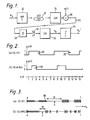
- a stream of binary data A k is recorded on a record carrier 10 such as an optical Compact Disc and subsequently read from the carrier 10 to generate a data stream A k ′ which is ideally an exact copy of the input stream A k .
- the recording and reproducing process involves several steps however which can introduce errors in the output data A k ′.
- a writing process 12 generates a pattern of marks on the record carrier which can be represented as a binary function s(t), where t represents distance along a track, or represents elapsed time when the marks are subsequently read by a relatively moving reading head.
- the writing process 12 may comprise an etching and stamping process for mass replication of records such as the currently available Compact Discs, or may for example comprise direct recording by an ablative, magneto-optical or phase-change technique such as those described in Chapter 6 of the first-mentioned reference (Bouwhuis et al ).
- Figure 2(a) shows a pattern s(t) that might be recorded on a record, against a scale of sampling periods or symbol intervals kT, where k is an integer and T is the length of each symbol interval.
- the land referenced 20 and the pit referenced 22 in Figure 2(a) are nominally the shortest land and pit that should be found in the pattern.
- the error E may arise for example from over- or under-etching at a stage in the mastering process of a Compact Disc.
- a recording in which the error E is positive (zeros too long) will be referred to as "over-etched” and a recording where E is negative will be referred to as "under-etched", whatever the actual cause of the error. It will be apparent that the error E is likely to remain constant, at least approximately, throughout any given recording.
- the perfectly square waveform s(t) becomes rounded and distorted by the reading process to produce a signal r(t).
- the reading process is modelled in Figure 1 by a Channel Impulse Response (CIR) 24 and by the addition of random noise n(t) at 26.
- the CIR represents principally the reading of the marks s(t) on the carrier 10 with (for example) a focussed radiation spot having a finite diameter.
- the noise n(t) represents random effects due for example to dirt and scratches, and also to focussing, tracking and timing errors.
- the signal r(t) is customarily filtered (at 28) to remove out-of-band noise and is then sampled every symbol interval T at 30 and passed through an equaliser 32 to produce a series of sample values a k .
- the equaliser is a sampled-data filter designed to compensate for the CIR 24 and so reduce inter-symbol interference. The design of such equalizers is described for example in the book “Digital Communications” by J. Proakis (McGraw-Hill, New York, 1983).
- the bit detector 34 is simply a threshold comparator for comparing a k with a threshold value u. Since the data stream is nominally d.c.-free, the threshold u can conveniently be derived by integrating A k ′ over a large number of symbol intervals, as in the known detector.
- E 0
- n(t) 0
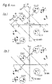
- the circles ('o') and crosses ('x') represent samples a k for which the intended bit values A k are zero and one respectively.
- the distribution of a k is not purely binary. This is because the radiation spot used for reading has a diameter which is in fact larger than the symbol interval T. In the Compact Disc system, for example, T represents 0.3 micron along the track and the laser spot diameter is nominally 1 micron. Therefore sampled values taken close to transitions in s(t), particularly within a minimum run-length pit or land, lie not at -1 or 1 but much closer to the threshold value u.
- the system is designed, however, to leave a clear decision margin M around the threshold u.
- the threshold u can be adjusted as shown to distinguish still between the circles and the crosses, but the decision margin M is severely reduced.
- the detector is more prone to make decision errors in response to the random noise n(t), and so the error-correcting capability afforded by the subsequent decoding stages will be heavily used correcting relatively minor errors (for example clocking and tracking errors), and will thus be less able to cope with errors caused by fingermarks, scratches etc. on the record carrier.
- relatively minor errors for example clocking and tracking errors
- decision margins are often much smaller than in the factory-produced CD's, so that systematic error is an even greater problem in such systems.
- the embodiments to be described implement methods which use a sample a k and the two adjacent samples a k-1 and a k+1 to determine the binary value A k ′ which is to be assigned to each sample k.
- the methods rely on the fact that with a minimum run length greater than T there is correlation between successive samples. For example, it is known that certain combinations (A k-1 , A k , A k+1 ) will simply not occur, namely (0,1,0) and (1,0,1). Such information can be used to improve the decision margin.
- the three sample values (a k-1 , a k , a k+1 ) can be visualised as coordinates of a point in a three-dimensional (3-D) space.
- An imaginary threshold surface would divide that space into two volumes and the bit value A k ′ could be assigned depending on which side of the surface a given sample point (a k-1 , a k , a k+1 ) fell.
- Such a technique would achieve the best possible decision margin using the three values available, but the complex calculations required make the 3-D technique expensive to adopt in a low cost apparatus. Accordingly, an economical embodiment of a method in accordance with the invention uses two steps with just two samples used in each step. This embodiment is illustrated in Figure 4 or Figure 5, depending on the type of systematic error present.
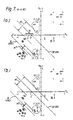
- Figures 6(a) and (b) are two-dimensional (2-D) scatter-plots illustrating the action of the two comparisons 42/52 and 44/54 respectively of the methods of Figures 4 and 5.
- the horizontal coordinate is a k
- the vertical coordinate is a k-1 .
- the threshold u and the decision margin M of the known simple threshold detector can therefore be marked as in Figure 6(a).
- the decision lines IV and V are perpendicular to those lines so that they offer the best decision margin.
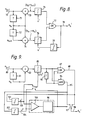
- Figure 8 shows a hardware bit detector suitable for implementing the 'OR' method of Figure 4 (E-positive case).
- the sample values a k-1 , a k , a k+1 arrive serially at the detector from the disc reading apparatus (as described above with reference to Figure 1) through an input 70.
- Two analogue delay circuits 71 and 72 are connected in series to the input 70. Each circuit 71 and 72 delays its input signal by one sample period T. Therefore when the value a k+1 is available for each sample k at the input 70, the values a k and a k-1 are available at the outputs of the first and second delay circuits 71 and 72 respectively as indicated in the Figure.
- a first summing circuit 73 receives the values a k+1 and a k from the input 70 and the output of the first delay circuit 71 and produces an output having a value a k + a k+1 . This value is fed to a first thresholding circuit (comparator) 75, which also receives a current threshold value u′. The output of the first thresholding circuit 75 thus carries the result of the second comparison 44 in the flowchart of Figure 4.
- a second summing circuit 74 receives the values a k and a k-1 from the outputs of the first and second delay circuits 71 and 72 respectively, and produces an output having a value a k-1 + a k . This value is fed to a second thresholding circuit (comparator) 76, which also receives the current threshold value u′. The output of the second thresholding circuit 76 thus carries the result of the first comparison 42 in the flowchart of Figure 4.
- the outputs of the two thresholding circuits 75 and 76 are fed to first and second inputs respectively of an OR gate 77 whose output 78 thus carries the binary value A k ′ which is assigned to each sample k.
- E is negative ("under-etched")
- the 'AND' method of Figure 5 can be implemented simply by changing the OR gate 77 to an AND gate.
- An integrator 79 is used to define the threshold value u′ for the thresholding circuits 75 and 76 in an adaptive fashion.
- the bit sequence A k ′ nominally contains as many ones as zeros, since the EFM-coded sequence A k ( Figure 1) is nominally d.c.-free.
- the integrator 79 serves to average A k ′ over many samples and varies the threshold u′ at its output as required to keep the balance between ones and zeros in the output sequence A k ′.
- Figure 9 shows an embodiment of a complete bit detector, which can select and implement the methods of Figure 4 and Figure 5.
- the embodiment of Figure 9 incorporates hardware-saving features and also means for determining the polarity of the systematic error E.
- the parts referenced 80, 81, 83, 85, 87 and 88 correspond to the parts referenced 70, 71, 73 etc. in the detector of Figure 8.
- second summing circuit or second thresholding circuit to correspond with the parts 72, 74 and 76 of Figure 8.
- These circuits can be omitted because the values a k-1 and a k for a given sample k are the same as the values a k and a k+1 for the previous sample. Therefore in Figure 8 the output of the second thresholding circuit 76 is simply a delayed version of the output of the first thresholding circuit 75.
- a single logic delay latch 92 is connected to the output of the sole thresholding circuit 85 to store the result of each comparison for one sampling period T to form the other comparison result for the next sample.
- the output of the latch 92 is connected to the second input of the OR gate 87.
- An AND gate 94 has first and second inputs connected in parallel with those of the OR gate 87 and has an output 95.
- a control circuit 96 controls an electronic switch 97 in order to connect either the output 88 of the OR gate 87 or the output 95 of the AND gate 94 to an output 98 which carries the output bit sequence A k ′.
- the control circuit 96 clearly requires knowledge of the polarity of the systematic error E in order to select the best position for the switch 97.
- Various techniques are possible for this.
- One possibility is to calculate the average of the sign of the sample values a k over a large number of samples.
- the technique embodied in the detector of Figure 9 is to use the version of the detector (i.e . the 'OR' or the 'AND' method) which has the lower magnitude of threshold value u′ or u ⁇ respectively.
- This is achieved by providing two integrators 101 and 102 connected to the outputs 88 and 95 of the OR and AND versions of the detector respectively.
- the values of u′ and u ⁇ are thus generated continuously and in parallel at the outputs 103 and 104 of the integrators and applied to inputs of a magnitude comparator 106 forming part of the control circuit 96.
- the method giving the lower magnitude threshold value is then selected by the control circuit 96 by operating the switch 97, and a further switch 108 is also provided to supply the appropriate threshold value u′ or u ⁇ to the threshold detector 85, as shown.
- the sequence of operation of the control circuit 96 is illustrated in the flow chart of Figure 10.
- control circuit 96 could arrange for a small part of a new recording to be read with the switch 97 in both positions and could then select the position which gave the lowest magnitude for the threshold value to be used for the playback of the rest of that recording.
- a disadvantage of using only one integrator is that it may be necessary to interrupt or delay playback to use each version of the detector in turn so as to enable a comparison of both versions to be made.
- Figures 9 and 10 with two integrators can adapt easily to changes in the polarity of the systematic error E by implementing the sequence of operations shown in Figure 10 continuously, or at least periodically, as indicated by the dashed flow path 110 in Figure 10.
- This may be advantageous for example when reproducing recordings made at differeent times or on different recording apparatuses, for example in writable/erasable recording technologies, in which E may vary significantly between different parts of the same record carrier. If this control sequence is to be implemented continuously, or at any great frequency, it may be advantageous to incorporate a degree of hysteresis into the comparison of the two threshold values. Otherwise, excessive switching between the two methods might occur when E is very close to zero and fluctuates in sign due to random variations.
- pattern of marks should be construed as including any detectable binary pattern, whether it is detectable optically or otherwise, and whether the marks are mechanical features as in the CD system or are variations in some other property of a recording medium as, for example, in phase-change and magneto-optical recording technologies.
- the method of the invention can be extended to make use of more than three adjacent samples.
- the extra decision margin gained (if any) will depend on the minimum run length in the particular pattern and also on the channel impulse response.
- the benefit obtainable by extending the method to use more than three samples is considered to be minimal with present channel characteristics.
Landscapes
- Engineering & Computer Science (AREA)
- Signal Processing (AREA)
- Optical Recording Or Reproduction (AREA)
- Signal Processing For Digital Recording And Reproducing (AREA)
Applications Claiming Priority (2)
| Application Number | Priority Date | Filing Date | Title |
|---|---|---|---|
| GB8826266A GB2224911A (en) | 1988-11-09 | 1988-11-09 | Method of and apparatus for assigning binary values to sample values |
| GB8826266 | 1988-11-09 |
Publications (3)
| Publication Number | Publication Date |
|---|---|
| EP0369518A2 true EP0369518A2 (de) | 1990-05-23 |
| EP0369518A3 EP0369518A3 (de) | 1991-08-21 |
| EP0369518B1 EP0369518B1 (de) | 1995-05-03 |
Family
ID=10646598
Family Applications (1)
| Application Number | Title | Priority Date | Filing Date |
|---|---|---|---|
| EP89202780A Expired - Lifetime EP0369518B1 (de) | 1988-11-09 | 1989-11-06 | Verfahren und Anordnung zur Zuweisung von binären Werten zu abgetasteten Werten |
Country Status (6)
| Country | Link |
|---|---|
| US (1) | US5151891A (de) |
| EP (1) | EP0369518B1 (de) |
| JP (1) | JP2870598B2 (de) |
| KR (1) | KR0148685B1 (de) |
| DE (1) | DE68922467T2 (de) |
| GB (1) | GB2224911A (de) |
Cited By (2)
| Publication number | Priority date | Publication date | Assignee | Title |
|---|---|---|---|---|
| EP0518782A3 (en) * | 1991-06-14 | 1993-03-31 | Sony Corporation | Bit detecting method and apparatus |
| WO1996033490A1 (fr) * | 1995-04-21 | 1996-10-24 | Thomson-Csf | Procede de lecture d'informations |
Families Citing this family (7)
| Publication number | Priority date | Publication date | Assignee | Title |
|---|---|---|---|---|
| JP3393407B2 (ja) * | 1992-01-28 | 2003-04-07 | ソニー株式会社 | ディスク状記録媒体のアドレス記録方法、ディスク状記録媒体のアドレス判別回路及びディスク記録再生装置 |
| US5251213A (en) * | 1992-05-12 | 1993-10-05 | Microcom Systems, Inc. | Multiport source routing token ring bridge apparatus |
| JPH07326139A (ja) * | 1994-06-01 | 1995-12-12 | Pioneer Electron Corp | 記録符号化ディジタル信号再生装置 |
| US6405141B1 (en) * | 2000-03-02 | 2002-06-11 | Ensco, Inc. | Dynamic track stiffness measurement system and method |
| KR20080104143A (ko) * | 2006-02-14 | 2008-12-01 | 코닌클리케 필립스 일렉트로닉스 엔.브이. | 광 디스크 판독용 비트 검출 |
| US9013821B1 (en) * | 2014-06-10 | 2015-04-21 | Western Digital Technologies, Inc. | Data storage device employing one-dimensional and two-dimensional channels |
| US9183877B1 (en) | 2015-03-20 | 2015-11-10 | Western Digital Technologies, Inc. | Data storage device comprising two-dimensional data dependent noise whitening filters for two-dimensional recording |
Family Cites Families (14)
| Publication number | Priority date | Publication date | Assignee | Title |
|---|---|---|---|---|
| BE755662A (fr) * | 1969-09-17 | 1971-02-15 | Burroughs Corp | Procede et appareil d'enregistrement et de detection magnetiques par modulation de frequence |
| US3988531A (en) * | 1975-04-02 | 1976-10-26 | Zenith Radio Corporation | System for compensating for incorrect duty factor when reading out information stored in a video disc |
| US4549288A (en) * | 1982-12-20 | 1985-10-22 | North American Philips Corporation | Apparatus for enhancing the playback signal in an optical data recording system |
| US4648085A (en) * | 1983-05-12 | 1987-03-03 | Nec Corporation | Optical information recording and reading apparatus with error correction |
| US4626670A (en) * | 1983-06-16 | 1986-12-02 | Xico, Inc. | Method and system for decoding time-varying, two-frequency, coherent-phase data |
| NL8303563A (nl) * | 1983-10-17 | 1985-05-17 | Philips Nv | Inrichting voor het weergeven van digitale informatie via een overdrachtsmedium. |
| US4688204A (en) * | 1984-11-16 | 1987-08-18 | Storage Technology Partners Ii | Pulsed optical data detection system |
| CA1275730C (en) * | 1985-03-05 | 1990-10-30 | Nec Corporation | Reading circuit in an optical disk apparatus |
| JPH0731877B2 (ja) * | 1985-07-03 | 1995-04-10 | 株式会社日立製作所 | 情報記録再生方法及び装置 |
| US4734900A (en) * | 1986-04-25 | 1988-03-29 | International Business Machines Corporation | Restoring and clocking pulse width modulated data |
| JP2810035B2 (ja) * | 1986-08-22 | 1998-10-15 | 株式会社日立製作所 | 光学的記録再生方法 |
| US4873680A (en) * | 1987-03-13 | 1989-10-10 | Laserdrive Ltd. | Apparatus and method for detecting and compensating for pit extension in an optical disk recording system |
| JPH0677371B2 (ja) * | 1987-10-19 | 1994-09-28 | 日本電気株式会社 | 記憶情報読出回路 |
| JP2513747B2 (ja) * | 1987-12-17 | 1996-07-03 | パイオニア株式会社 | デ―タ記録再生方法 |
-
1988
- 1988-11-09 GB GB8826266A patent/GB2224911A/en not_active Withdrawn
-
1989
- 1989-10-25 US US07/427,674 patent/US5151891A/en not_active Expired - Lifetime
- 1989-11-06 EP EP89202780A patent/EP0369518B1/de not_active Expired - Lifetime
- 1989-11-06 DE DE68922467T patent/DE68922467T2/de not_active Expired - Fee Related
- 1989-11-07 KR KR1019890016072A patent/KR0148685B1/ko not_active Expired - Fee Related
- 1989-11-08 JP JP1288935A patent/JP2870598B2/ja not_active Expired - Fee Related
Cited By (4)
| Publication number | Priority date | Publication date | Assignee | Title |
|---|---|---|---|---|
| EP0518782A3 (en) * | 1991-06-14 | 1993-03-31 | Sony Corporation | Bit detecting method and apparatus |
| US5313472A (en) * | 1991-06-14 | 1994-05-17 | Sony Corporation | Bit detecting method and apparatus |
| WO1996033490A1 (fr) * | 1995-04-21 | 1996-10-24 | Thomson-Csf | Procede de lecture d'informations |
| CN1114915C (zh) * | 1995-04-21 | 2003-07-16 | 汤姆森多媒体公司 | 读取信息的方法及其系统 |
Also Published As
| Publication number | Publication date |
|---|---|
| KR900008495A (ko) | 1990-06-03 |
| JP2870598B2 (ja) | 1999-03-17 |
| EP0369518A3 (de) | 1991-08-21 |
| KR0148685B1 (ko) | 1998-10-15 |
| EP0369518B1 (de) | 1995-05-03 |
| JPH02173976A (ja) | 1990-07-05 |
| DE68922467T2 (de) | 1996-01-11 |
| GB8826266D0 (en) | 1988-12-14 |
| DE68922467D1 (de) | 1995-06-08 |
| US5151891A (en) | 1992-09-29 |
| GB2224911A (en) | 1990-05-16 |
Similar Documents
| Publication | Publication Date | Title |
|---|---|---|
| US6842410B1 (en) | Digital automatic gain control of a multilevel optical disc read signal | |
| US4945538A (en) | Method and apparatus for processing sample values in a coded signal processing channel | |
| KR100550510B1 (ko) | 부분 응답 채널에서 노이즈 상관을 감소시키기 위한 방법과 장치 | |
| KR100465361B1 (ko) | 데이터복호장치 | |
| JP3558168B2 (ja) | 光学式情報再生装置 | |
| KR0156485B1 (ko) | 부호간 간섭에 의한 신호파형왜곡의 보정기능을 갖는 데이타 변별장치 | |
| US5151891A (en) | Method and apparatus for assigning binary values to sample values of a waveform representing a pattern of recording marks on a record carrier | |
| JP3956436B2 (ja) | データ復調方法及びこれを用いた光ディスク装置 | |
| US5952944A (en) | Modulation device and demodulation device and methods of the same | |
| JP3788684B2 (ja) | 波形等化器及びこれを用いたデータ再生装置 | |
| JP3432003B2 (ja) | 情報再生装置及び情報記録再生装置 | |
| EP0853805B1 (de) | Übertragung, aufzeichnung und wiedergabe eines digitalen informationssignals | |
| KR19990018221A (ko) | 고밀도 데이타 저장기기를 위한 피알엠엘 코드의 부호화 및복호화 방법 | |
| KR100751972B1 (ko) | 가변 임계값을 갖는 매체 잡음 포스트-프로세서 | |
| US6233214B1 (en) | Information data recording/reproducing method | |
| JP2002184132A (ja) | D=2光チャネル用データ処理装置および方法 | |
| JP4040116B2 (ja) | ディスク装置、データ伝送装置及び直流レベル測定回路 | |
| JP3370367B2 (ja) | 波形等化方法、装置及びそれを備えた光ディスク装置 | |
| JP2888187B2 (ja) | 情報検出装置 | |
| Verboom | Selective inter-symbol-interference cancellation (SISIC) for high-density optical recording using d= 1 channel code | |
| JP3983450B2 (ja) | 再生装置と再生回路 | |
| KR20000034470A (ko) | 디브이디 재생장치의 적응 등화기 | |
| KR100202545B1 (ko) | 기록매체의 재생신호 판정 장치 및 방법 | |
| Kobayashi et al. | High-track-density optical disc by radial direction partial response | |
| KR100240338B1 (ko) | 개선된 광디스크 재생 시스템 |
Legal Events
| Date | Code | Title | Description |
|---|---|---|---|
| PUAI | Public reference made under article 153(3) epc to a published international application that has entered the european phase |
Free format text: ORIGINAL CODE: 0009012 |
|
| AK | Designated contracting states |
Kind code of ref document: A2 Designated state(s): DE FR GB IT |
|
| PUAL | Search report despatched |
Free format text: ORIGINAL CODE: 0009013 |
|
| AK | Designated contracting states |
Kind code of ref document: A3 Designated state(s): DE FR GB IT |
|
| 17P | Request for examination filed |
Effective date: 19920221 |
|
| 17Q | First examination report despatched |
Effective date: 19930329 |
|
| GRAA | (expected) grant |
Free format text: ORIGINAL CODE: 0009210 |
|
| AK | Designated contracting states |
Kind code of ref document: B1 Designated state(s): DE FR GB IT |
|
| PG25 | Lapsed in a contracting state [announced via postgrant information from national office to epo] |
Ref country code: IT Free format text: LAPSE BECAUSE OF FAILURE TO SUBMIT A TRANSLATION OF THE DESCRIPTION OR TO PAY THE FEE WITHIN THE PRESCRIBED TIME-LIMIT;WARNING: LAPSES OF ITALIAN PATENTS WITH EFFECTIVE DATE BEFORE 2007 MAY HAVE OCCURRED AT ANY TIME BEFORE 2007. THE CORRECT EFFECTIVE DATE MAY BE DIFFERENT FROM THE ONE RECORDED. Effective date: 19950503 |
|
| REF | Corresponds to: |
Ref document number: 68922467 Country of ref document: DE Date of ref document: 19950608 |
|
| ET | Fr: translation filed | ||
| PLBE | No opposition filed within time limit |
Free format text: ORIGINAL CODE: 0009261 |
|
| STAA | Information on the status of an ep patent application or granted ep patent |
Free format text: STATUS: NO OPPOSITION FILED WITHIN TIME LIMIT |
|
| 26N | No opposition filed | ||
| REG | Reference to a national code |
Ref country code: FR Ref legal event code: CD |
|
| REG | Reference to a national code |
Ref country code: GB Ref legal event code: IF02 |
|
| PGFP | Annual fee paid to national office [announced via postgrant information from national office to epo] |
Ref country code: DE Payment date: 20040121 Year of fee payment: 15 |
|
| REG | Reference to a national code |
Ref country code: GB Ref legal event code: 746 Effective date: 20040811 |
|
| REG | Reference to a national code |
Ref country code: FR Ref legal event code: D6 |
|
| PGFP | Annual fee paid to national office [announced via postgrant information from national office to epo] |
Ref country code: FR Payment date: 20041125 Year of fee payment: 16 |
|
| PGFP | Annual fee paid to national office [announced via postgrant information from national office to epo] |
Ref country code: GB Payment date: 20041129 Year of fee payment: 16 |
|
| PG25 | Lapsed in a contracting state [announced via postgrant information from national office to epo] |
Ref country code: DE Free format text: LAPSE BECAUSE OF NON-PAYMENT OF DUE FEES Effective date: 20050601 |
|
| PG25 | Lapsed in a contracting state [announced via postgrant information from national office to epo] |
Ref country code: GB Free format text: LAPSE BECAUSE OF NON-PAYMENT OF DUE FEES Effective date: 20051106 |
|
| GBPC | Gb: european patent ceased through non-payment of renewal fee |
Effective date: 20051106 |
|
| PG25 | Lapsed in a contracting state [announced via postgrant information from national office to epo] |
Ref country code: FR Free format text: LAPSE BECAUSE OF NON-PAYMENT OF DUE FEES Effective date: 20060731 |
|
| REG | Reference to a national code |
Ref country code: FR Ref legal event code: ST Effective date: 20060731 |