EP0370252A2 - Optisches Übertragungssystem - Google Patents
Optisches Übertragungssystem Download PDFInfo
- Publication number
- EP0370252A2 EP0370252A2 EP89119728A EP89119728A EP0370252A2 EP 0370252 A2 EP0370252 A2 EP 0370252A2 EP 89119728 A EP89119728 A EP 89119728A EP 89119728 A EP89119728 A EP 89119728A EP 0370252 A2 EP0370252 A2 EP 0370252A2
- Authority
- EP
- European Patent Office
- Prior art keywords
- signal
- optical
- main
- optical fiber
- correction
- Prior art date
- Legal status (The legal status is an assumption and is not a legal conclusion. Google has not performed a legal analysis and makes no representation as to the accuracy of the status listed.)
- Granted
Links
- 230000003287 optical effect Effects 0.000 title claims abstract description 84
- 238000004891 communication Methods 0.000 title claims abstract description 20
- 239000013307 optical fiber Substances 0.000 claims abstract description 46
- 238000012937 correction Methods 0.000 claims description 19
- 230000005540 biological transmission Effects 0.000 abstract description 20
- 239000004065 semiconductor Substances 0.000 description 34
- 239000000306 component Substances 0.000 description 11
- 238000000034 method Methods 0.000 description 3
- 238000010586 diagram Methods 0.000 description 2
- 230000000694 effects Effects 0.000 description 2
- 238000001514 detection method Methods 0.000 description 1
- 230000006866 deterioration Effects 0.000 description 1
- 230000002542 deteriorative effect Effects 0.000 description 1
- 238000011161 development Methods 0.000 description 1
- 239000000835 fiber Substances 0.000 description 1
- 238000003780 insertion Methods 0.000 description 1
- 230000037431 insertion Effects 0.000 description 1
- 230000001105 regulatory effect Effects 0.000 description 1
Images

Classifications
-
- H—ELECTRICITY
- H04—ELECTRIC COMMUNICATION TECHNIQUE
- H04B—TRANSMISSION
- H04B10/00—Transmission systems employing electromagnetic waves other than radio-waves, e.g. infrared, visible or ultraviolet light, or employing corpuscular radiation, e.g. quantum communication
- H04B10/50—Transmitters
- H04B10/58—Compensation for non-linear transmitter output
-
- H—ELECTRICITY
- H04—ELECTRIC COMMUNICATION TECHNIQUE
- H04B—TRANSMISSION
- H04B10/00—Transmission systems employing electromagnetic waves other than radio-waves, e.g. infrared, visible or ultraviolet light, or employing corpuscular radiation, e.g. quantum communication
- H04B10/50—Transmitters
- H04B10/501—Structural aspects
- H04B10/503—Laser transmitters
- H04B10/504—Laser transmitters using direct modulation
-
- H—ELECTRICITY
- H04—ELECTRIC COMMUNICATION TECHNIQUE
- H04B—TRANSMISSION
- H04B10/00—Transmission systems employing electromagnetic waves other than radio-waves, e.g. infrared, visible or ultraviolet light, or employing corpuscular radiation, e.g. quantum communication
- H04B10/50—Transmitters
- H04B10/501—Structural aspects
- H04B10/503—Laser transmitters
- H04B10/505—Laser transmitters using external modulation
- H04B10/5059—Laser transmitters using external modulation using a feed-forward signal generated by analysing the optical or electrical input
- H04B10/50593—Laser transmitters using external modulation using a feed-forward signal generated by analysing the optical or electrical input to control the modulating signal amplitude including amplitude distortion
-
- H—ELECTRICITY
- H04—ELECTRIC COMMUNICATION TECHNIQUE
- H04B—TRANSMISSION
- H04B10/00—Transmission systems employing electromagnetic waves other than radio-waves, e.g. infrared, visible or ultraviolet light, or employing corpuscular radiation, e.g. quantum communication
- H04B10/50—Transmitters
- H04B10/516—Details of coding or modulation
- H04B10/54—Intensity modulation
- H04B10/541—Digital intensity or amplitude modulation
Definitions
- the present invention relates to an optical communication system, and more particularly to an optical communication system in which analog signals are transmitted by optical communication system by directly amplitude modulation, suppressing the modulation distortion of the modulated signals by a feed forward control.
- optical CATV optical cable television systems
- FM system wide band frequency modulation system
- VSB/AM system residual side band amplitude modulation system
- S/N signal to noise
- the FM system is such that in order to transmit the signals in the optical fiber, it is necessary to provide a AM/FM converter for converting the electrical amplitude modulation signal into the FM signal, further it is necessary to provide a FM/AM converter for converting the FM signal received from the optical fiber into electrical AM signal. Therefore, the communication system is expensive. To the contrary, the VSB/AM system does not require such AM/FM converter and FM/AM converter and the communication system is inexpensive and simple in structure.
- the optical signals are generated by modulating the amplitude of the current applied to a semiconductor laser.
- the relation between the input current and the light output power of the light emitting unit such as a semiconductor laser is generally non linear, high order harmonic distortion is contained in the wave shape of the light output, resulting in lowering CN ratio which is similar to S/N ratio.
- the output power of the semiconductor laser can not increase proportional to the increment of the input current to the semiconductor laser, but the output of the semiconductor contains modulation distortion proportional to the square and cube of the applied current to the semiconductor laser.
- optical FF method Another way is so called feed forward method (referred to as optical FF method hereinafter) disclosed in the literature "ANALOG TRANSMISSION OF TV-CHANNELS ON OPTICAL FIBER , WITH NON-LINEARITIES CORRECTION BY REGULATED FEED FORWARD' FRANKART. J.P. et al. REV. H.F. ELECTRON TELECOMMUNICATION VOL. 12 NO. 9 1984.
- the signals to be transmitted are applied to a semiconductor laser, and the main light signals obtained by the semiconductor laser are compared with a part of the original electric signals so as to obtain correction signals. Then a feed forward control is performed by adding the correction signals to the main received light signals after detection so that the modulation distortion generated in the semiconductor laser is suppressed.
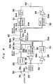
- Fig. 1 shows a general structure of an optical communication system employing the optical feed forward system.
- the electric analog signal Se to be transmitted is divided into two analog signals Se1 and Se2 by a branch unit 1 and one of the signals Se1 drives a main semiconductor laser 2, which generates amplitude-modulated optical signals.
- a part of the optical signal is derived from the optical signal by an optical branch unit 3, being converted into an electrical signal Se3 by an auxiliary light receiving element 9.
- Another signal Se2 divided by the electric branch unit 1 and the electric signal Se3 converted by the auxiliary light receiving element 9 have their phases and amplitudes adjusted by a delay line 6 and an amplifier 10, thereafter both signals Se2 and Se3 are subtracted by a combiner 8, whereby an electric signal Sd corresponding to the high order harmonic distortion component of the semiconductor laser 2 is formed in the combiner 8.
- the electric signal Sd is amplified by an amplifier 11 and thereafter drives a correction light emitting unit 12, thus correction light signal So2 is formed.
- the correction light signal So2 (referred to as distortion signal) is transmitted by an optical fiber line 13.
- the remainder optical signal So1 taken out from the optical branch unit 3 is transmitted by an optical fiber line 4.
- the distortion signal So2 and the main signal So1 transmitted by the respective optical fiber lines are converted into electric signals Se4 and Se5 by the light receiving elements 5 and 14.
- the respective electric signals Se4 and Se5 have their phase and amplitude adjusted by a delay line 16 and an amplifier 15 and thereafter summed in a combiner 17 so as to eliminate the modulation distortion, whereby an analog signal Se without the modulation distortion can be reproduced.
- the optical fiber lines become expensive and the wide band property of the optical fiber can not be effectively used.
- An essential object of the present invention is to provide an optical communication system in which the optical feed forward system can be realized by one optical fiber line.
- an optical communication system of the optical feed forward type in which the main signal and the distortion signal are transmitted by a common optical fiber line from the transmission part to the reception part.
- the communication system according to the present invention is suitable for a long distance multi channel optical fiber communication such as so called a CATV and a picture transmission.
- the optical communication system shown in Fig. 2 basically comprises a main semiconductor laser 20 for generating optical signals by amplitude-modulating the carrier light of the laser 20 in response to the amplitude of analog signals to be transmitted (referred to as transmission signal hereinafter), an optical fiber line 22 for transmitting the amplitude-modulated optical signal and a light receiving element 21 for reproducing the optical signal transmitted by the optical fiber line 22 in the electric signal.
- the main semiconductor laser 20 there is used a semiconductor laser of Fabry-Perot type with an isolater, oscillating at the wavelength of ⁇ 1 such as 1.3 ⁇ m and as the light receiving element 21, a PIN photo diode made of In Ga As is used.
- an optical divider 24 which branches a part of the optical signal generated from the main semiconductor laser 20 at the port 24b connected to a branch line 26 and an optical multiplexer 40 for applying the distortion signal So2 to the optical fiber line 22.
- an optical demultiplexer 41 for branching the distortion signal So2 in ⁇ 2 band from the main signal in ⁇ 1 band both transmitted by the optical fiber line 22.
- a transmission signal branch unit 35 for branching a part of the transmission electrical signal is provided on a connection line which connects the transmission signal input port and the main semiconductor laser 20.
- the transmission signal branch unit 35 is also connected to the transmission signal branch line 25.
- a delay line 27 is provided on the transmission signal branch line 25 and is ended by a subtracting point or a combiner circuit 36.
- a PIN photo diode made of In Ga As is used.
- the output terminal of the amplifier 29 is connected to the combiner 36.
- the combiner 36 performs a subtraction between the output signal of the delay line 27 and the output signal of the amplifier 28s, after the phase of both output signals are adjusted to coincide each other by the delay line 27 and the amplitude of both output signals are adjusted to coincide each other by the amplifier 28, producing an electric signal Sd representing the high order harmonic distortion component generated in the amplitude-modulation performed in the main semiconductor laser 20.
- An amplifier 29 of a variable gain type is connected to the output terminal of the combiner 36 and the output of the amplifier 29 is connected to a semiconductor laser 31 (referred to as correction semiconductor laser).
- the correction semiconductor laser 31 there is used a DFB semiconductor laser which generates light of wavelength ⁇ 2 for example 1.54 ⁇ m.
- the correction semiconductor laser 31 generates a distortion signal or correction light signal, which is an amplitude-modulated optical signal corresponding to the output of the amplifier 29.
- the distortion signal So2 is applied to the optical fiber line 22 through the optical multiplexer 40.
- the optical demultiplexer 41 connected to the optical fiber line 22 branches the distortion signal of wavelength ⁇ 2 and the branched distortion signal is transmitted to a correcting light receiving element 32.
- a correcting light receiving element 32 there is used a PIN photo diode made of In Ga As which converts the distortion signal of ⁇ 2 into an electric signal.
- the converted electric signal corresponds to the high order harmonic distortion component mentioned above.
- An amplifier 34 is connected to the output terminal of the correcting light receiving element 32.
- the light receiving element 21 is connected to the output terminal of the optical demultiplexer 41 which outputs the main signal of the wavelength of ⁇ 1 and the light receiving element 21 outputs an electric signal corresponding to the main signal So1.
- a delay line 33 is connected to the output terminal of the light receiving element 21.
- the delay line 33 and the amplifier 34 are connected to a combiner 42.
- the electrical signal corresponding to the main signal So1 and the electric signal corresponding to the high order harmonic distortion component are synthesized, after they are adjusted in terms of the phase and amplitude, so that the modulation distortion which occurs at the time of amplitude modulation in the main semiconductor laser 20 can be eliminated.
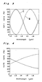
- the optical multiplexer 40 and optical demultiplexer 41 it is desired to use such an optical fiber coupler having optical multiplex and demultiplexing properties as shown in Fig. 3.
- the property I shown in the real line can be obtained between the ports 40a and 40c of the multiplexer 40 and 41a and 41c of the demultiplexer 41, for transmission of the optical signals of 1,3 ⁇ m band
- the property II shown in the dotted lines can be obtained between the ports 40b and 40c of the multiplexer 40 and 41b and 41c of the demultiplexer 41 for transmission of the optical signals of 1,55 ⁇ m band.
- optical fiber coupler there may be used such optical fiber coupler as disclosed in a literature entitled “RECENT OPTICAL FIBER COUPLER TECHNICS” in “OPTRONICS” vol. 5 pages 125 to 126.
- the optical fiber coupler disclosed in the literature can be formed with the insertion loss less than 1 dB for the light of wavelengths 1.3 ⁇ m and 1.55 ⁇ m. Therefore, CN ratio at the output of the combiner 42 is not deteriorated.
- the transmission signal Se is branched in two analog signals Se1 and Se2 by the signal branch unit 35.
- the analog signal Se1 drives the main semiconductor laser 20 and is converted into the amplitude-modulated optical signal of 1.3 ⁇ m band. A part of the optical signal is taken out by the optical divider 24 and is converted into the electric signal Se3 by the light receiving element 30.
- the analog signal Se2 branched by the branch unit 35 is applied to the delay line 27 and the phase of the signal Se2 is adjusted to coincide with the phase of the output signal of the amplifier 28, being applied to the combiner 36.
- the signal Se3 is applied to the amplifier 28 and the amplitude of the signal Se3 is adjusted to coincide with the amplitude of the output signal of the delay circuit 27, being applied to the combiner 36. Both output signals of Se2 and Se3 are subtracted, whereby the electric signal Sd corresponding to the high order harmonic distortion component generated in the main semiconductor laser 20 can be formed.
- the electric signal Sd is amplified by the amplifier 29, then drives the semiconductor laser 31 so that the semiconductor laser 31 generates the distortion signal So2 which is the amplitude-modulated optical signal in 1.55 ⁇ m band modulated by the high order harmonic distortion mentioned above.
- the distortion signal So2 is applied in the optical fiber line 22 through the optical multiplexer 40 and transmitted thereby.
- the main signal So1 taken out by the optical divider 24 is transmitted by the same optical fiber line 22.
- the distortion optical signal So2 transmitted by the optical fiber line 22 is separated by the optical demultiplexer 41 and transmitted to the correcting light receiving element 32, whereby the distortion signal So2 is converted or demodulated into the electric signal Se5 representing the high order harmonic distortion by the light receiving element 32.
- the main signal So1 transmitted by the optical fiber line 22 is converted or demodulated into the electric signal Se4 by the light receiving element 21.
- the electric signals Se4 and Se5 are, after their phase and amplitude are adjusted by the delay line 33 and the amplifier 34, summed by the combiner 42 to eliminate the modulation distortion, whereby the analog signal Se without the modulation distortion can be reproduced.
- the optical fiber line 22 was a conventional single mode optical fiber for 1.3 ⁇ m with 10 km long.
- the main semiconductor laser 20 was modulated by sine wave of 70 MHz whereby it was possible to decrease by 10 dB of the modulation distortion of secondary harmonic component of 140 MHz compared in case where the feed forward system was not used.
- the optical fiber line 22 is accommodated in the constant temperature bath, changing the temperature in the range from -40°C to +85°C, the variation of the secondary order harmonic component was small lower than 1 dB at the combiner 42.
- the present invention in which the main signal and the distortion signal are transmitted in the same optical fiber line is superior to the prior art optical feed forward system which the main signal and the distortion signal are transmitted by separate optical fiber cable lines.
- the present invention is not limited to the embodiment described above but can be modified in various ways.
- a combination of the phase adjusting circuit and the amplitude adjusting circuit in the respective input circuits of the combiners 36 and 42 may be used.
- optical multiplexer and/or demultiplexer there may be used an optical coupler of 1.3 ⁇ m wavelength range with 50 % split ratio as shown in Fig. 4, if the attenuation of the signal of about 6 dB can be allowed.
- the wavelength ⁇ 1 of the light of the main semiconductor laser for the main signal is different from the wavelength ⁇ 2 of the semiconductor laser for correction for generating the distortion signal
- semiconductor lasers which generate light of the same wavelength band.
- optical multiplexer and demultiplexer which separate optical signals of similar wavelengths.
Landscapes
- Physics & Mathematics (AREA)
- Electromagnetism (AREA)
- Engineering & Computer Science (AREA)
- Computer Networks & Wireless Communication (AREA)
- Signal Processing (AREA)
- Optics & Photonics (AREA)
- Nonlinear Science (AREA)
- Optical Communication System (AREA)
Applications Claiming Priority (2)
| Application Number | Priority Date | Filing Date | Title |
|---|---|---|---|
| JP63297487A JP2610667B2 (ja) | 1988-11-25 | 1988-11-25 | 光通信システム |
| JP297487/88 | 1988-11-25 |
Publications (3)
| Publication Number | Publication Date |
|---|---|
| EP0370252A2 true EP0370252A2 (de) | 1990-05-30 |
| EP0370252A3 EP0370252A3 (de) | 1992-01-22 |
| EP0370252B1 EP0370252B1 (de) | 1996-08-28 |
Family
ID=17847139
Family Applications (1)
| Application Number | Title | Priority Date | Filing Date |
|---|---|---|---|
| EP89119728A Expired - Lifetime EP0370252B1 (de) | 1988-11-25 | 1989-10-24 | Optisches Übertragungssystem |
Country Status (4)
| Country | Link |
|---|---|
| EP (1) | EP0370252B1 (de) |
| JP (1) | JP2610667B2 (de) |
| CA (1) | CA1328695C (de) |
| DE (1) | DE68927040T2 (de) |
Cited By (3)
| Publication number | Priority date | Publication date | Assignee | Title |
|---|---|---|---|---|
| EP0416424A3 (en) * | 1989-09-06 | 1991-12-04 | General Instrument Corporation | Apparatus and method for reducing distortion in an analog optical transmission system |
| EP0475376A3 (en) * | 1990-09-12 | 1992-12-09 | General Instrument Corporation | Apparatus and method for linearizing the operation of an external optical modulator |
| WO2002025844A1 (en) * | 2000-09-21 | 2002-03-28 | Nokia Corporation | Method and system for transmitting a signal via a non-linear transmission unit |
Families Citing this family (3)
| Publication number | Priority date | Publication date | Assignee | Title |
|---|---|---|---|---|
| JPH10145297A (ja) | 1996-11-08 | 1998-05-29 | Nec Corp | フィードフォワード歪補償方式 |
| TW432234B (en) * | 1997-08-20 | 2001-05-01 | Advantest Corp | Optical signal transmission apparatus and method |
| US7657189B2 (en) * | 2004-12-17 | 2010-02-02 | Raytheon Company | Optical link |
Family Cites Families (1)
| Publication number | Priority date | Publication date | Assignee | Title |
|---|---|---|---|---|
| DE3632047C2 (de) * | 1986-09-20 | 1998-05-14 | Sel Alcatel Ag | Optisches Nachrichtenübertragungssystem für Schmalband- und Breitband-Nachrichtensignale |
-
1988
- 1988-11-25 JP JP63297487A patent/JP2610667B2/ja not_active Expired - Lifetime
-
1989
- 1989-09-29 CA CA000614725A patent/CA1328695C/en not_active Expired - Fee Related
- 1989-10-24 DE DE68927040T patent/DE68927040T2/de not_active Expired - Fee Related
- 1989-10-24 EP EP89119728A patent/EP0370252B1/de not_active Expired - Lifetime
Cited By (4)
| Publication number | Priority date | Publication date | Assignee | Title |
|---|---|---|---|---|
| EP0416424A3 (en) * | 1989-09-06 | 1991-12-04 | General Instrument Corporation | Apparatus and method for reducing distortion in an analog optical transmission system |
| EP0475376A3 (en) * | 1990-09-12 | 1992-12-09 | General Instrument Corporation | Apparatus and method for linearizing the operation of an external optical modulator |
| WO2002025844A1 (en) * | 2000-09-21 | 2002-03-28 | Nokia Corporation | Method and system for transmitting a signal via a non-linear transmission unit |
| WO2002025843A1 (en) * | 2000-09-21 | 2002-03-28 | Nokia Corporation | Method and system for transmitting a signal via a non-linear transmission unit |
Also Published As
| Publication number | Publication date |
|---|---|
| JPH02143733A (ja) | 1990-06-01 |
| DE68927040D1 (de) | 1996-10-02 |
| DE68927040T2 (de) | 1997-02-06 |
| JP2610667B2 (ja) | 1997-05-14 |
| EP0370252B1 (de) | 1996-08-28 |
| EP0370252A3 (de) | 1992-01-22 |
| CA1328695C (en) | 1994-04-19 |
Similar Documents
| Publication | Publication Date | Title |
|---|---|---|
| US5153763A (en) | CATV distribution networks using light wave transmission lines | |
| AU673223B2 (en) | An optical communications system for transmitting infomation signals having different wavelengths over a same optical fiber | |
| US5257124A (en) | Low distortion laser system for AM fiber optic communication | |
| EP0595140B1 (de) | Verfahren zur Linearisierung eines unsymmetrischen Mach Zehnder optischen Frequenzdiskriminators | |
| US5262883A (en) | CATV distribution networks using light wave transmission lines | |
| US5107360A (en) | Optical transmission of RF subcarriers in adjacent signal bands | |
| EP0503512A2 (de) | Verfahren und Vorrichtung zur Übertragung von amplituden-modulierten Signalen über eine optische Übertragungleitung | |
| US7474150B2 (en) | Amplifier composite triple beat (CTB) reduction by phase filtering | |
| US20060165413A1 (en) | DWDM CATV return system with up-converters to prevent fiber crosstalk | |
| HK1008453B (en) | Method for linearizing an unbalanced mach zehnder optical frequency discriminator | |
| EP0473667A1 (de) | Optisches nachrichtennetz. | |
| EP1168682A2 (de) | Hochfrequenz-Sender mit einer Verzerrungskompensationfunktion für optische Übertragung | |
| EP0168914B1 (de) | Optisches Übertragungssystem | |
| US5289550A (en) | Modulated light source with a linear transfer function and method utilizing same | |
| US5214524A (en) | Optical communication system | |
| WO2001003339A1 (en) | Pre-shaping laser modulation signals to increase modulation index | |
| EP0606170A2 (de) | Optisches Nachrichtenübertragungssystem und darin verwendete optische Netzwerkendstellen | |
| EP0370252B1 (de) | Optisches Übertragungssystem | |
| EP1060583A1 (de) | Optische verbindungen | |
| JPH06315010A (ja) | 光伝送装置 | |
| CA2024566A1 (en) | Apparatus and method for reducing distortion in an analog optical transmission system | |
| JPH0115179B2 (de) | ||
| JP2950814B1 (ja) | 光副搬送波伝送システム | |
| JPH0423532A (ja) | サブキャリア多重光伝送方法 | |
| JP3097106B2 (ja) | サブキャリア多重光伝送方法 |
Legal Events
| Date | Code | Title | Description |
|---|---|---|---|
| PUAI | Public reference made under article 153(3) epc to a published international application that has entered the european phase |
Free format text: ORIGINAL CODE: 0009012 |
|
| AK | Designated contracting states |
Kind code of ref document: A2 Designated state(s): DE FR GB IT |
|
| 17P | Request for examination filed |
Effective date: 19901220 |
|
| PUAL | Search report despatched |
Free format text: ORIGINAL CODE: 0009013 |
|
| AK | Designated contracting states |
Kind code of ref document: A3 Designated state(s): DE FR GB IT |
|
| 17Q | First examination report despatched |
Effective date: 19940913 |
|
| GRAH | Despatch of communication of intention to grant a patent |
Free format text: ORIGINAL CODE: EPIDOS IGRA |
|
| GRAA | (expected) grant |
Free format text: ORIGINAL CODE: 0009210 |
|
| GRAH | Despatch of communication of intention to grant a patent |
Free format text: ORIGINAL CODE: EPIDOS IGRA |
|
| AK | Designated contracting states |
Kind code of ref document: B1 Designated state(s): DE FR GB IT |
|
| ITF | It: translation for a ep patent filed | ||
| REF | Corresponds to: |
Ref document number: 68927040 Country of ref document: DE Date of ref document: 19961002 |
|
| ET | Fr: translation filed | ||
| PLBE | No opposition filed within time limit |
Free format text: ORIGINAL CODE: 0009261 |
|
| STAA | Information on the status of an ep patent application or granted ep patent |
Free format text: STATUS: NO OPPOSITION FILED WITHIN TIME LIMIT |
|
| 26N | No opposition filed | ||
| PGFP | Annual fee paid to national office [announced via postgrant information from national office to epo] |
Ref country code: FR Payment date: 19991011 Year of fee payment: 11 |
|
| PGFP | Annual fee paid to national office [announced via postgrant information from national office to epo] |
Ref country code: GB Payment date: 19991020 Year of fee payment: 11 |
|
| PGFP | Annual fee paid to national office [announced via postgrant information from national office to epo] |
Ref country code: DE Payment date: 19991022 Year of fee payment: 11 |
|
| PG25 | Lapsed in a contracting state [announced via postgrant information from national office to epo] |
Ref country code: GB Free format text: LAPSE BECAUSE OF NON-PAYMENT OF DUE FEES Effective date: 20001024 |
|
| GBPC | Gb: european patent ceased through non-payment of renewal fee |
Effective date: 20001024 |
|
| PG25 | Lapsed in a contracting state [announced via postgrant information from national office to epo] |
Ref country code: FR Free format text: LAPSE BECAUSE OF NON-PAYMENT OF DUE FEES Effective date: 20010629 |
|
| PG25 | Lapsed in a contracting state [announced via postgrant information from national office to epo] |
Ref country code: DE Free format text: LAPSE BECAUSE OF NON-PAYMENT OF DUE FEES Effective date: 20010703 |
|
| REG | Reference to a national code |
Ref country code: FR Ref legal event code: ST |
|
| PG25 | Lapsed in a contracting state [announced via postgrant information from national office to epo] |
Ref country code: IT Free format text: LAPSE BECAUSE OF NON-PAYMENT OF DUE FEES;WARNING: LAPSES OF ITALIAN PATENTS WITH EFFECTIVE DATE BEFORE 2007 MAY HAVE OCCURRED AT ANY TIME BEFORE 2007. THE CORRECT EFFECTIVE DATE MAY BE DIFFERENT FROM THE ONE RECORDED. Effective date: 20051024 |