EP0370302B1 - Mehrstufiger Kaskadengleichrichter - Google Patents
Mehrstufiger Kaskadengleichrichter Download PDFInfo
- Publication number
- EP0370302B1 EP0370302B1 EP89120634A EP89120634A EP0370302B1 EP 0370302 B1 EP0370302 B1 EP 0370302B1 EP 89120634 A EP89120634 A EP 89120634A EP 89120634 A EP89120634 A EP 89120634A EP 0370302 B1 EP0370302 B1 EP 0370302B1
- Authority
- EP
- European Patent Office
- Prior art keywords
- cascade
- rectifier
- stage
- capacitors
- stages
- Prior art date
- Legal status (The legal status is an assumption and is not a legal conclusion. Google has not performed a legal analysis and makes no representation as to the accuracy of the status listed.)
- Expired - Lifetime
Links
- 239000003990 capacitor Substances 0.000 claims description 19
- 238000009499 grossing Methods 0.000 claims description 6
- 238000004804 winding Methods 0.000 description 5
- 238000010276 construction Methods 0.000 description 2
- 238000005516 engineering process Methods 0.000 description 1
Images

Classifications
-
- H—ELECTRICITY
- H02—GENERATION; CONVERSION OR DISTRIBUTION OF ELECTRIC POWER
- H02M—APPARATUS FOR CONVERSION BETWEEN AC AND AC, BETWEEN AC AND DC, OR BETWEEN DC AND DC, AND FOR USE WITH MAINS OR SIMILAR POWER SUPPLY SYSTEMS; CONVERSION OF DC OR AC INPUT POWER INTO SURGE OUTPUT POWER; CONTROL OR REGULATION THEREOF
- H02M7/00—Conversion of AC power input into DC power output; Conversion of DC power input into AC power output
- H02M7/02—Conversion of AC power input into DC power output without possibility of reversal
- H02M7/04—Conversion of AC power input into DC power output without possibility of reversal by static converters
- H02M7/06—Conversion of AC power input into DC power output without possibility of reversal by static converters using discharge tubes without control electrode or semiconductor devices without control electrode
- H02M7/10—Conversion of AC power input into DC power output without possibility of reversal by static converters using discharge tubes without control electrode or semiconductor devices without control electrode arranged for operation in series, e.g. for multiplication of voltage
- H02M7/103—Containing passive elements (capacitively coupled) which are ordered in cascade on one source
Definitions
- the invention relates to a multi-stage cascade rectifier with a smoothing capacitor column and two shear capacitor columns connected symmetrically thereto.
- Such a multi-stage cascade rectifier is known for example from CH-PS 335 750.
- a series connection of a number of capacitors corresponding to the number of stages is connected as a so-called smoothing capacitor column to the center tap of the secondary winding of a high-voltage transformer which is at zero potential.
- two further series connections of capacitors, the so-called shear capacitor columns, are connected to the secondary winding.
- Each cascade stage is designed as a full-wave rectifier stage by appropriate wiring with high-voltage diodes.
- Known cascade rectifiers such as those used in particular as high-voltage generators for supplying X-ray tubes in X-ray technology, are designed for the highest type performance, that is the product of maximum output voltage and maximum output current. This means that the high-voltage transformer, inverter and power electronics must be designed for this output power. If you work with lower output voltages and increased load currents in accordance with the output power, the primary winding of the high-voltage transformer must be designed for the correspondingly high current load.
- the task is to further develop the known multi-stage cascade rectifier by circuit measures that are as simple as possible so that the circuit complexity is reduced.
- a solution to the problem is seen in a multi-stage cascade rectifier of the type mentioned, in which in at least one pair of switches for switching off the following cascades is arranged in the thrust capacitor columns.
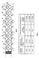
- FIG. 4 shows the current loads in the different switching phases.
- the cascade rectifier shown in FIG. 1 with eight stages I ... VIII for voltage multiplication consists of a high-voltage transformer TR, the secondary winding of which is provided with a center tap at zero potential.
- a series connection of capacitors C1, referred to as smoothing capacitor column GS is connected to the center tap, the number of which corresponds to that of the cascade stages.
- two further series connections of capacitors C2 are connected symmetrically to the smoothing capacitor column GS as so-called shear capacitor columns SS.
- four rectifier diodes are connected so that a full-wave rectifier circuit is formed.
- a pair of switches S1, S1 'and S2, S2' are arranged in each case in the push-capacitor capacitor columns before stage IV and stage VI, with which the following cascade stages can be switched off.
Landscapes
- Engineering & Computer Science (AREA)
- Power Engineering (AREA)
- Rectifiers (AREA)
- X-Ray Techniques (AREA)
Description
- Die Erfindung bezieht sich auf einen mehrstufigen Kaskadengleichrichter mit einer Glättungskondensatorsäule und zwei symmetrisch dazu geschalteten Schubkondensatorsäulen.
- Ein derartiger mehrstufiger Kaskadengleichrichter ist beispielsweise aus der CH-PS 335 750 bekannt. Eine Reihenschaltung einer der Stufenzahl entsprechenden Anzahl von Kondensatoren ist als sogenannte Glättungskondensatorsäule an die auf Nullpotential liegende Mittelanzapfung der Sekundärwicklung eines Hochspannungstrafos angeschlossen. Symmetrisch dazu sind zwei weitere Reihenschaltungen von Kondensatoren, die sogenannten Schubkondensatorsäulen, an der Sekundärwicklung angeschlossen. Jede Kaskadenstufe ist durch entsprechende Beschaltung mit Hochspannungsdioden als Vollweggleichrichterstufe ausgebildet.
- Bekannte Kaskadengleichrichter, wie sie insbesondere als Hochspannungsgeneratoren für die Versorgung von Röntgenröhren in der Röntgentechnik eingesetzt werden, sind konstruktiv auf die höchste Typenleistung, das ist das Produkt aus maximaler Ausgangsspannung und maximalem Ausgangsström, ausgelegt. Das bedeutet, daß Hochspannungstransformator, Wechselrichter und Leistungselektronik für diese Ausgangsleistung ausgelegt sein müssen.
Wird mit kleineren Ausgangsspannungen und entsprechend der Ausgangsleistung erhöhten Lastströmen gearbeitet, muß die Primärwicklung des Hochspannungstransformators für die entsprechend hohe Strombelastung ausgelegt werden. - Es besteht die Aufgabe, durch möglichst einfache Schaltungsmaßnahmen den bekannten mehrstufigen Kaskadengleichrichter so weiterzubilden, daß der Schaltungsaufwand verringert wird.
- Eine Lösung der Aufgabe wird in einem mehrstufigen Kaskadengleichrichter der eingangs genannten Art gesehen, bei dem in den Schubkondensatorsäulen mindestens ein Schalterpaar zur Abschaltung der folgenden Kaskaden angeordnet ist.
Damit wird eine geringere Strombelastung im Primärkreis bei höheren Lastströmen erreicht, so daß der Bauaufwand für Hochspannungstransformator, Wechselrichter und Leistungselektronik verringert werden kann, oder es besteht die Möglichkeit, bei gleichem Bauaufwand die Strombelastung und die Ausgangsspannung zu erhöhen. - Zur Erläuterung der Erfindung ist in den Figuren 1 bis 3 ein Ausführungsbeispiel in den verschiedenen Schaltphasen dargestellt.
In der Tabelle der Figur 4 sind die Strombelastungen in den verschiedenen Schaltphasen einander gegenübergestellt. - Der in der Figur 1 gezeigte Kaskadengleichrichter mit acht Stufen I ... VIII zur Spannungsvervielfachung besteht, wie bekannt, aus einem Hochspannungstransformator TR, dessen Sekundärwicklung mit einer auf Nullpotential liegenden Mittelanzapfung versehen ist.
An die Mittelanzapfung ist eine als Glättungskondensatorsäule GS bezeichnete Reihenschaltung von Kondensatoren C1 angeschlossen, deren Anzahl der der Kaskadenstufen entspricht. An den äußeren Anschlüssen der Sekundärwicklung des Hochspannungstransformators TR sind symmetrisch zu der Glättungskondensatorsäule GS zwei weitere Reihenschaltungen von Kondensatoren C2 als sogenannte Schubkondensatorsäulen SS angeschlossen. In jeder Kaskadenstufe I ... VIII sind vier Gleichrichterdioden so geschaltet, daß jeweils eine Vollweggleichrichterschaltung gebildet wird.
Zur erfindungsgemäßen Abschaltung von Kaskadenstufen ist hier vor der Stufe IV und der Stufe VI jeweils ein Schalterpaar S1, S1' bzw. S2, S2' in den Schubkondensatorsäulen angeordnet, mit denen die jeweils folgenden Kaskadenstufen abschaltbar sind. - Werden, wie Figur 2 zeigt, die Schalter S2, S2' geöffnet, so sind nur noch fünf Kaskadenstufen in Betrieb bei entsprechend niedrigerer Ausgangsspannung und höherem Ausgangsstrom. Soll der Kaskadengleichrichter nur mit drei Stufen betrieben werden, so ist das Schalterpaar S1, S1' geöffnet, S2, S2' kann offen oder geschlossen sein.
- In der Tabelle in Figur 4 sind für das gezeigte Ausführungsbeispiel eines achtstufigen Kaskadengleichrichters die Werte bei unterschiedlichen Ausgangsspannungen und Lastströmen aufgezeigt. Man erkennt, daß bei einer Ausgangsspannung von 20 kV und einem Laststrom von 150 mA der Primärstrom im Hochspannungstransformator bei der dreistufig geschalteten Kaskade um mehr als die Hälfte geringer ist als bei der herkömmlichen Schaltung.
Claims (1)
- Mehrstufiger Kaskadengleichrichter mit einer an die sekundärseitige Mittelanzapfung eines Hochspannungstransformators angeschlossenen Reihenschaltung von Glättungskondensatoren (Glättungskondensatorsäule) und zwei symmetrisch dazu geschalteten Reihenschaltungen von Schubkondensatoren (Schubkondensatorsäulen), wobei jede Kaskade aus einer Vollweggleichrichterschaltung besteht, dadurch gekennzeichnet, daß in den Schubkondensatorsäulen (SS) mindestens ein Schalterpaar (S1, S1') zur Abschaltung der folgenden Kaskadenstufen angeordnet ist.
Applications Claiming Priority (2)
| Application Number | Priority Date | Filing Date | Title |
|---|---|---|---|
| DE3839310A DE3839310A1 (de) | 1988-11-21 | 1988-11-21 | Mehrstufiger kaskadengleichrichter |
| DE3839310 | 1988-11-21 |
Publications (3)
| Publication Number | Publication Date |
|---|---|
| EP0370302A2 EP0370302A2 (de) | 1990-05-30 |
| EP0370302A3 EP0370302A3 (en) | 1990-10-03 |
| EP0370302B1 true EP0370302B1 (de) | 1993-08-11 |
Family
ID=6367574
Family Applications (1)
| Application Number | Title | Priority Date | Filing Date |
|---|---|---|---|
| EP89120634A Expired - Lifetime EP0370302B1 (de) | 1988-11-21 | 1989-11-07 | Mehrstufiger Kaskadengleichrichter |
Country Status (2)
| Country | Link |
|---|---|
| EP (1) | EP0370302B1 (de) |
| DE (2) | DE3839310A1 (de) |
Families Citing this family (2)
| Publication number | Priority date | Publication date | Assignee | Title |
|---|---|---|---|---|
| DE4115294C2 (de) * | 1991-05-10 | 1995-03-16 | Telefunken Microelectron | Schaltung zur Spannungsüberhöhung |
| EP2207405B1 (de) * | 2006-08-31 | 2013-10-16 | Koninklijke Philips N.V. | Kaskade zweier Spannungsquellen zur Spannungsversorgung eines Röntgengerätes |
Family Cites Families (2)
| Publication number | Priority date | Publication date | Assignee | Title |
|---|---|---|---|---|
| CH335750A (de) * | 1955-03-29 | 1959-01-31 | Haefely & Cie Ag Emil | Mehrstufiger Kaskadengleichrichter |
| GB1564401A (en) * | 1976-09-29 | 1980-04-10 | Atomic Energy Authority Uk | High voltage electrical power supply |
-
1988
- 1988-11-21 DE DE3839310A patent/DE3839310A1/de not_active Withdrawn
-
1989
- 1989-11-07 EP EP89120634A patent/EP0370302B1/de not_active Expired - Lifetime
- 1989-11-07 DE DE8989120634T patent/DE58905257D1/de not_active Expired - Fee Related
Also Published As
| Publication number | Publication date |
|---|---|
| DE3839310A1 (de) | 1990-05-23 |
| EP0370302A3 (en) | 1990-10-03 |
| EP0370302A2 (de) | 1990-05-30 |
| DE58905257D1 (de) | 1993-09-16 |
Similar Documents
| Publication | Publication Date | Title |
|---|---|---|
| EP1311058B1 (de) | Frequenzumrichter | |
| EP0802617A2 (de) | Leistungselektronische Schaltungsanordnung | |
| EP0660496B1 (de) | Umrichteranordnung mit niederinduktivem Kommutierungskreis | |
| EP1186091B1 (de) | Spannungszwischenkreis-umrichter | |
| DE3872439T2 (de) | Pulsbreitenmodulationsumwandler. | |
| DE2214950A1 (de) | Schaltungsanordnung zum Aneinander schalten von mindestens zwei Wicklungen | |
| DE1961195A1 (de) | Wechselrichterschaltung | |
| DE3125240C2 (de) | Gleichhochspannungsgenerator | |
| EP1501180A1 (de) | Umrichterschaltung | |
| DE3035305C2 (de) | Wechselrichterschaltung für einen Dreiphasen-Synchronmotor | |
| EP0751612A2 (de) | Stromrichterschaltungsanordnung | |
| EP0370302A2 (de) | Mehrstufiger Kaskadengleichrichter | |
| DE102015105889A1 (de) | Schaltmodul und Umrichter mit wenigstens einem Schaltmodul | |
| DE4121177C2 (de) | ||
| EP0515380B1 (de) | Wechselstromquelle zum schweissen | |
| DE10138751B4 (de) | Wechselrichter mit schnellschaltenden ansteuerbaren elektronischen Schaltern, insbesondere IGBT-Schaltern, sowie Verfahren zur Ansteuerung eines derartigen Wechselrichters | |
| EP0669702B1 (de) | Oberwellen-Aktivfilter für eine Umrichterschaltung | |
| DE202020101549U1 (de) | Schaltungsanordnung mit mehreren Leistungselektronikmodulen | |
| DE69407637T2 (de) | Leistungsversorgung mit mindestens zwei schaltenden Brücken | |
| DE3509853C2 (de) | ||
| DE4403908C1 (de) | Gegentaktschaltstufe | |
| DE69818415T2 (de) | Hochspannungsschalter aus reihengeschalteten resonanten Zellen | |
| DE3430308A1 (de) | Stromrichter | |
| DE2843087C2 (de) | ||
| DE913439C (de) | Selbstgefuehrter Einphasen-Kontaktwechselrichter |
Legal Events
| Date | Code | Title | Description |
|---|---|---|---|
| PUAI | Public reference made under article 153(3) epc to a published international application that has entered the european phase |
Free format text: ORIGINAL CODE: 0009012 |
|
| AK | Designated contracting states |
Kind code of ref document: A2 Designated state(s): CH DE ES FR GB IT LI NL |
|
| PUAL | Search report despatched |
Free format text: ORIGINAL CODE: 0009013 |
|
| AK | Designated contracting states |
Kind code of ref document: A3 Designated state(s): CH DE ES FR GB IT LI NL |
|
| 17P | Request for examination filed |
Effective date: 19901026 |
|
| 17Q | First examination report despatched |
Effective date: 19921208 |
|
| GRAA | (expected) grant |
Free format text: ORIGINAL CODE: 0009210 |
|
| AK | Designated contracting states |
Kind code of ref document: B1 Designated state(s): CH DE ES FR GB IT LI NL |
|
| PG25 | Lapsed in a contracting state [announced via postgrant information from national office to epo] |
Ref country code: ES Free format text: THE PATENT HAS BEEN ANNULLED BY A DECISION OF A NATIONAL AUTHORITY Effective date: 19930811 |
|
| REF | Corresponds to: |
Ref document number: 58905257 Country of ref document: DE Date of ref document: 19930916 |
|
| ITF | It: translation for a ep patent filed | ||
| GBT | Gb: translation of ep patent filed (gb section 77(6)(a)/1977) |
Effective date: 19931027 |
|
| ET | Fr: translation filed | ||
| PLBE | No opposition filed within time limit |
Free format text: ORIGINAL CODE: 0009261 |
|
| STAA | Information on the status of an ep patent application or granted ep patent |
Free format text: STATUS: NO OPPOSITION FILED WITHIN TIME LIMIT |
|
| 26N | No opposition filed | ||
| PGFP | Annual fee paid to national office [announced via postgrant information from national office to epo] |
Ref country code: GB Payment date: 19941018 Year of fee payment: 6 |
|
| PGFP | Annual fee paid to national office [announced via postgrant information from national office to epo] |
Ref country code: FR Payment date: 19941117 Year of fee payment: 6 |
|
| PGFP | Annual fee paid to national office [announced via postgrant information from national office to epo] |
Ref country code: NL Payment date: 19941130 Year of fee payment: 6 |
|
| PGFP | Annual fee paid to national office [announced via postgrant information from national office to epo] |
Ref country code: CH Payment date: 19950216 Year of fee payment: 6 |
|
| PG25 | Lapsed in a contracting state [announced via postgrant information from national office to epo] |
Ref country code: GB Effective date: 19951107 |
|
| PG25 | Lapsed in a contracting state [announced via postgrant information from national office to epo] |
Ref country code: LI Effective date: 19951130 Ref country code: CH Effective date: 19951130 |
|
| PG25 | Lapsed in a contracting state [announced via postgrant information from national office to epo] |
Ref country code: NL Effective date: 19960601 |
|
| GBPC | Gb: european patent ceased through non-payment of renewal fee |
Effective date: 19951107 |
|
| REG | Reference to a national code |
Ref country code: CH Ref legal event code: PL |
|
| PG25 | Lapsed in a contracting state [announced via postgrant information from national office to epo] |
Ref country code: FR Effective date: 19960731 |
|
| NLV4 | Nl: lapsed or anulled due to non-payment of the annual fee |
Effective date: 19960601 |
|
| REG | Reference to a national code |
Ref country code: FR Ref legal event code: ST |
|
| PGFP | Annual fee paid to national office [announced via postgrant information from national office to epo] |
Ref country code: DE Payment date: 20011127 Year of fee payment: 13 |
|
| PG25 | Lapsed in a contracting state [announced via postgrant information from national office to epo] |
Ref country code: DE Free format text: LAPSE BECAUSE OF NON-PAYMENT OF DUE FEES Effective date: 20030603 |
|
| PG25 | Lapsed in a contracting state [announced via postgrant information from national office to epo] |
Ref country code: IT Free format text: LAPSE BECAUSE OF NON-PAYMENT OF DUE FEES;WARNING: LAPSES OF ITALIAN PATENTS WITH EFFECTIVE DATE BEFORE 2007 MAY HAVE OCCURRED AT ANY TIME BEFORE 2007. THE CORRECT EFFECTIVE DATE MAY BE DIFFERENT FROM THE ONE RECORDED. Effective date: 20051107 |