EP0370432B1 - Hocheschwindigkeitsdifferentialleseverstärker zur Verwendung mit Eintransistorspeicherzellen - Google Patents
Hocheschwindigkeitsdifferentialleseverstärker zur Verwendung mit Eintransistorspeicherzellen Download PDFInfo
- Publication number
- EP0370432B1 EP0370432B1 EP89121444A EP89121444A EP0370432B1 EP 0370432 B1 EP0370432 B1 EP 0370432B1 EP 89121444 A EP89121444 A EP 89121444A EP 89121444 A EP89121444 A EP 89121444A EP 0370432 B1 EP0370432 B1 EP 0370432B1
- Authority
- EP
- European Patent Office
- Prior art keywords
- bit line
- transistor
- handling terminal
- precharge
- memory
- Prior art date
- Legal status (The legal status is an assumption and is not a legal conclusion. Google has not performed a legal analysis and makes no representation as to the accuracy of the status listed.)
- Expired - Lifetime
Links
- 238000000034 method Methods 0.000 claims description 5
- 238000010586 diagram Methods 0.000 description 6
- WABPQHHGFIMREM-IGMARMGPSA-N lead-207 Chemical compound [207Pb] WABPQHHGFIMREM-IGMARMGPSA-N 0.000 description 4
- 238000003491 array Methods 0.000 description 3
- WABPQHHGFIMREM-OUBTZVSYSA-N lead-208 Chemical compound [208Pb] WABPQHHGFIMREM-OUBTZVSYSA-N 0.000 description 2
- 230000001052 transient effect Effects 0.000 description 2
- 238000010276 construction Methods 0.000 description 1
- 238000012986 modification Methods 0.000 description 1
- 230000004048 modification Effects 0.000 description 1
Images


Classifications
-
- G—PHYSICS
- G11—INFORMATION STORAGE
- G11C—STATIC STORES
- G11C7/00—Arrangements for writing information into, or reading information out from, a digital store
- G11C7/06—Sense amplifiers; Associated circuits, e.g. timing or triggering circuits
-
- G—PHYSICS
- G11—INFORMATION STORAGE
- G11C—STATIC STORES
- G11C16/00—Erasable programmable read-only memories
- G11C16/02—Erasable programmable read-only memories electrically programmable
- G11C16/06—Auxiliary circuits, e.g. for writing into memory
- G11C16/26—Sensing or reading circuits; Data output circuits
- G11C16/28—Sensing or reading circuits; Data output circuits using differential sensing or reference cells, e.g. dummy cells
Definitions
- This invention pertains to memory devices, and more particularly, to sense amplifiers for use in determining the data stored in single transistor memory cells, such as EPROM memory cells.
- EEPROM devices are well known in the prior art and may be categorized broadly into two groups: those memory arrays which employ memory cells utilizing a single transistor and those memory arrays which employ memory cells which utilize two transistors.
- the advantage in utilizing two transistors per memory cell is that a differential output signal may be obtained which can be sensed by a differential sense amplifier, providing greater speed of operation and less susceptibility to errors caused by noise.
- utilizing two transistors per memory cell consumes a greater amount of surface area in an integrated circuit than memory devices utilizing a single transistor per memory cell.
- FIGURE 1 depicts a schematic diagram of a memory device utilizing an array of two transistor memory cells and a differential sense amplifier. For convenience, only a single memory cell formed of transistors 11 and 12 is shown, although it is well known in the art how such memory arrays comprising a plurality of memory cells, each containing two transistors, are formed and selectively addressed.
- floating gate transistors 11 and 12 each include a floating gate which is selectively charged to increase the control gate threshold voltage of the transistor to correspond to a logical zero, as compared with the control gate threshold voltage of a transistor having substantially no charge placed on its floating gate and corresponding to a logical one.
- transistors 11 and 12 are erased to be in the low threshold voltage state, i.e., each having a threshold voltage corresponding to a logical one. Then, during programming, either transistor 11 or 12 is programmed by placing a charge on its floating gate in order to increase its threshold voltage to correspond to a logical zero, thereby providing a differential data signal on BIT and BIT lines 18 and 19, which is in turn applied to the differential input leads of differential sense amplifier 20.
- Differential sense amplifier in turn provides a single ended output signal on output terminal 21 which is capable of being provided more quickly and with less susceptibility to noise and variations of voltage levels on leads 18 and 19 than is possible if a single ended sense amplifier were used, as depicted in the prior art structure of Figure 2.
- Table 1 depicts the operation of memory cell 10 during the erase and programming modes. Table 1 Programmed State V T Transistor 11 BIT V T Transistor 12 BIT erased low 1 low 1 0 low 1 high 0 1 high 0 low 1
- another type of memory array is constructed of a plurality of memory cells, each containing a single floating gate transistor, such as transistor 31. Again, for simplicity, the entire array of memory cells is not shown, such construction being well known to those of ordinary skill in the art.
- BIT line 35 is connected to the input lead of single ended sense amplifier 37, which is inherently slower (due to its responding to a single ended input signal which changes voltage in one direction with respect to a reference voltage) and more susceptible to noise and variations in voltage levels on BIT line 35 (due to its lack of common mode noise rejection) than is the differential sense amplifier 20 of Figure 1 having its input leads connected to both BIT and BIT lines.
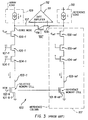
- FIG. 3 The prior art circuit of Figure 3 has combined the use of a memory array having a plurality of memory cells, each containing a single floating gate transistor, with the higher speed and lower susceptibility to noise of a differential sense amplifier.
- Figure 3 shows only a single memory cell formed of transistor 101-N-1 associated with row line 102-N and BIT line 103-1. It is readily understood by those of ordinary skill in the art that the memory array actually includes a plurality of N row lines and M BIT lines, and a plurality of NxM uniquely addressable single transistor memory cells.
- row line 102-N is enabled by placing a read voltage having a voltage greater than the control gate threshold voltage of a memory array transistor which is programmed to the logical one state (no charge on its floating gate), and less than the control gate threshold voltage of a memory array transistor which is programmed to a logical zero state (a charge placed on its floating gate).
- BIT line 103-1 is selected by turning on column select transistors 104-1 and 105-1 and applying reference voltage VREF to the gate of transistor 106-1. As shown in Figure 3, transistors 104-1 and 105-1 serve as column select transistors connected in an AND configuration. Other addressing techniques or the use of other than two select transistors 104-1, 105-1, are well known in the art.
- the reference voltage applied to the gate of transistor 106-1 is approximately 2.5 to 3 volts and causes transistor 106-1 to precharge the selected column 103-1.
- memory array transistor 101-N-1 stores a logical one, it turns on when selected for reading, causing differential sense amplifier input lead 107 to be connected to ground.
- memory array transistor 101-N-1 stores a logical zero it does not turn on when selected for reading due to its higher control gate threshold voltage.
- input lead 107 of differential sense amplifier 111 is not connected to ground, and the current I/2 supplied by array load current source 109 is not discharged to ground but is made available on high impedance input lead 107 of differential sense amplifier 111.
- multiplexing techniques can be used to multiplex a plurality of columns to a single differential sense amplifier, or to multiplex a plurality of output leads from a plurality of differential sense amplifiers to a single output lead of an integrated circuit.
- reference set 117 includes a reference unprogrammed memory cell 101-N-REF (storing a logical one) and having its control gate connected to row line 102-N.
- reference set 117 includes reference transistors 104-REF and 105-REF corresponding to column select transistors 104-1 and 105-1, respectively, with their control gates connected to VCC (typically 5 volts).
- Reference set 117 also includes transistor 106-REF having its control gate connected to reference voltage VREF, serving as an analog to transistor 106 1.
- Reference load current source 110 provides a current I equal to twice the current provided by array load current source 109.
- Balancing transistor 118 serves to connect the inverting and noninverting input leads of differential sense amplifier 111 prior to sensing the data stored in the selected memory cell.
- balancing transistor 118 is a P channel transistor controlled by a signal BAL applied to its gate electrode which goes high when sensing is to be performed following selection of a desired row and column defining the single memory cell to be sensed by differential sense amplifier 111.
- differential input lead 107 When memory array transistor 101-N-1 stores a logical zero and is selected for reading, differential input lead 107 is not connected to ground and thus when balancing is terminated (i.e., when transistor 118 turns off):
- ⁇ V107 the rate of change of the voltage on differential input lead 107
- V108 the constant reference voltage to be compared to the voltage of sense node 107
- I The reference current through reference Bit line 103-REF
- C107 the capacitance on input lead 107
- dv dt the time rate of change of the differential input voltage between differential input leads 107 and 108.
- a memory circuit as defined in the preamble of patent claim 1 and a method as defined in the preamble of patent claim 9 are known from NEW ELECTRONICS, vol. 18, no. 22, Nov. 1985, p.70,73,74.
- the precharge sub-circuit as defined in claims 4 through 8 is known per se from EP-A-0 154 547.
- a novel circuit is provided as indicated in claim 1. It allows a differential sense amplifier to be utilized in conjunction with a memory array comprised of a plurality of memory cells each containing a single transistor, as well as a reference bit line including a reference memory cell.
- a differential input signal is applied to the sense amplifier based upon the binary data stored in an addressed memory cell at a rate equal to or greater than the differential input signal available in prior art differential memory cells having two transistors per cell. This is accomplished by precharging the selected bit line and the reference bit line, and then selecting the word line of the memory cell to be read, while causing the reference memory cell to conduct.
- the differential voltage between the selected bit line and the reference bit line is then sensed to determine the state of the data stored in the selected memory cell.
- the ratio of currents through the selected bit line and the reference bit line is selected to be other than one, in order to achieve a rapid differential voltage swing, and rapid reading of the data stored within the selected memory cell.
- FIG. 4 One embodiment of a memory array circuit constructed in accordance with the teachings of this invention is shown in the schematic diagram of Figure 4.
- a single memory array transistor 201-N-1 is shown, although it is to be understood that the memory array comprises a plurality of such memory cells having their sources connected in common, their drains connected in common, and their control gates connected to individual row lines such as row line 202-N.
- Connected between BIT line 203-1 and differential input lead 207 are column select transistors 205-1 and 204-1 and transistor 206-1 having its gate connected to reference voltage VREF, as in the prior art embodiment of Figure 3.
- reference set 217 includes transistors 204-REF, 205-REF and 206-REF corresponding to transistors 204-1, 205-1, and 206-1, respectively, as in the case of a prior art circuit of Figure 3.
- the gates of transistors 204-REF and 205-REF are connected to VCC (typically 5 volts)and the gate of transistor 206-REF is connected to reference voltage VREF.
- reference memory array transistor cell 202-REF has its control gate connected to a balancing signal BAL .
- transistors 251 through 254 are used to precharge BIT line 203-1 and reference line 203-REF.
- precharge signal P and balancing signal BAL go low, thereby turning off reference cell 202-REF and turning on P channel transistors 251 and 252.
- the source of P channel transistor 252 is connected to VCC. Since memory cell transistor 201-N-1 has been selected for reading, column select transistors 204-1 and 205-1 are turned on, as is transistor 206-1, and thus BIT line 203-1 is precharged via conducting P channel transistors 252 and 254.
- differential input leads 207 and 208 are precharged to a voltage level of VCC-VTP, where:
- balance signal BAL goes high, thus turning on reference cell transistor 202-REF and turning off balancing transistor 251.
- transistors 253 and 254 need not be made very large, but only sufficiently large to conduct currents I2 and I3, respectively. However, should transistor 253 be made rather large, a slight transient voltage will appear on differential input lead 207 when the BAL goes high and balancing transistor 251 turns off. If this occurs, it is preferable to wait a short period of time to allow the transient voltage on lead 207 to settle prior to sensing the stored data being addressed. Typically, when a relatively large transistor 253 is used, one need only wait 5 to 10 nanoseconds or so after balancing transistor 251 turns off prior to sensing the state of the stored data.
- a novel memory circuit which provides a differential signal which develops at a rate equal to or greater than that of a true differential signal developed utilizing a two transistor memory cell.
Landscapes
- Read Only Memory (AREA)
- Semiconductor Memories (AREA)
- Static Random-Access Memory (AREA)
Claims (9)
- Eine Speicherschaltung umfassend eine Mehrzahl von Bitleitungen (203-1), eine Mehrzahl von Wortleitungen (202-N), eine Mehrzahl von Speicherzellen (201-N-1), wobei jede Speicherzelle nur einem Bitleitungs-Wortleitungspaar zugeordnet ist, Mittel (204-1), (205-1) für das Adressieren einer ausgewählten Bitleitung, Mittel für das Adressieren einer ausgewählten Wortleitung, eine Referenzbitleitung (203-ref), einschließlich einer Referenzspeicherzelle (202-ref), einen Leseverstärker (211) mit einem ersten Eingangsleiter (207) für den Anschluß an einer ausgewählten Bitleitung, einen zweiten Eingangsleiter (208) für den Anschluß an die Referenzbitleitung und einem Ausgangsleiter (212) für die Bereitstellung eines Ausgangssignals, das indikativ ist für den Logikzustand der in einer ausgewählten Speicherzelle gespeicherten Daten, definiert durch die ausgewählte Bitleitung und die ausgewählte Wortleitung, Ausgleichsmittel (251) für das selektive Bewirken, daß der erste und der zweite Eingangsleiter auf demselben Spannungspegel sind, ein Vorladungsquellenmittel (252) für das Bereitstellen eines Vorladesignals, erste Mittel (253) für das Anlegen des Vorladesignals an die ausgewählte Bitleitung, wodurch ein Ladestrom (I2) einer ausgewählten Bitleitung bereitgestellt wird und zweite Mittel (254) für das Anlegen des Vorladesignals an die Referenzbitleitung, wodurch ein Referenzbitleitungsladestrom (I3) bereitgestellt wird, welche Speicherschaltung dadurch gekennzeichnet ist, daß das erste und das zweite Mittel (253, 254) für das Anschießen bemessen sind zum Bereitstellen eines vorbestimmten Stromverhältnisses (I3/I2), das größer als eins ist zwischen dem Referenzbitleitungsladestrom (I3) und dem Bitleitungsladestrom (I2).
- Eine Speicherkomponente nach Anspruch 1, ferner dadurch gekennzeichnet, daß die Referenzspeicherzelle einen Speichertransistor (202-ref) umfaßt, der auf einen ersten Logikzustand programmiert ist mit einer Source, angeschlossen an die Referenzbitleitung (203-ref), einem Drain, an dem ein ausgewählter Spannungspegel liegt und einem Steuergate, beaufschlagt mit einem Steuersignal (
BAL ). - Eine Speicherkomponente nach Anspruch 2, ferner dadurch gekennzeichnet, daß das Steuersignal dazu dient, selektiv die Durchschaltung des Referenztransistors zu bewirken und außerdem dazu dient, selektiv das Ausgleichsmittel (251) zu veranlassen, daß der erste und der zweite Eingangsleiter auf denselben Spannungspegel kommen.
- Eine Speicherkomponente nach Anspruch 1, ferner dadurch gekennzeichnet, daß die Vorladequelle einen Transistor (252) umfaßt mit einer Eingangsstromverarbeitungsklemme, angeschlossen an eine Spannungsquelle mit einer Ausgangsstromverarbeitungsklemme für das Bereitstellen des Vorladesignals und einem Steuergate, beaufschlagt mit einem Vorladesteuersignal (
P ). - Eine Speicherkomponente nach Anspruch 4, ferner dadurch gekennzeichnet, daß das erste Mittel für das Anlegen eine erste Stromhandhabungsklemme umfaßt, verbunden mit der Ausgangsstromhandhabungsklemme der Vorladequelle und eine zweite Stromhandhabungsklemme, verbunden mit der ausgewählten Bitleitung.
- Eine Speicherkomponente nach Anspruch 4, ferner dadurch gekennzeichnet, daß das erste Mittel für das Anschließen einen Transistor (253) umfaßt mit einer ersten Stromhandhabungsklemme, verbunden mit der Ausgangsstromhandhabungsklemme der Vorladequelle einer zweiten Stromhandhabungsklemme, verbunden mit der ausgewählten Bitleitung und einem Steuergate, verbunden mit der ausgewählten Bitleitung.
- Eine Speicherkomponente nach Anspruch 5, ferner dadurch gekennzeichnet, daß das zweite Mittel für das Anschließen eine erste Stromhandhabungsklemme umfaßt, verbunden mit der Ausgangsstromhandhabungsklemme der Vorladequelle und eine zweite Stromhandhabungsklemme, verbunden mit der Referenzbitleitung.
- Eine Speicherkomponente nach Anspruch 6, ferner dadurch gekennzeichnet, daß das zweite Anschlußmittel einen Transistor (254) umfaßt, mit einer ersten Stromhandhabungsklemme, verbunden mit der Ausgangsstromhandhabungsklemme der Vorladequelle, mit einer zweiten Stromhandhabungsklemme, verbunden mit der Referenzbitleitung und mit einem Steuergate, verbunden mit der ausgewählten Bitleitung.
- Ein Betriebsverfahren einer Speicherkomponente, umfassend eine Mehrzahl von Bitleitungen (203-1), eine Mehrzahl von Wortleitungen (202-N), eine Mehrzahl von Speicherzellen (201-N-1), wobei jede Speicherzelle einem einzigen Bitleitungs-Wortleitungspaar zugeordnet ist, mit Mitteln für (204-1, 205-1) Adressieren einer ausgewählten Bitleitung, Mitteln für Adressieren einer ausgewählten Wortleitung mit einer Referenzbitleitung (203-ref), einschließlich einer Referenzspeicherzelle (202-ref), mit einem Leseverstärker (211) mit einem ersten Eingangsleiter (207) für Anschluß an eine ausgewählte Bitleitung, einem zweiten Eingangsleiter (208) für Anschluß an die Referenzbitleitung und einem Ausgangsleiter (212) für die Bereitstellung eines Ausgangssignals, das indikativ ist für den Logikzustand der in einer ausgewählten Speicherzelle gespeicherten Daten, welche definiert wird durch die ausgewählte Bitleitung und die ausgewählte Wortleitung, mit Ausgleichsmitteln (251) für das selektive Herbeiführen gleichen Spannungspegels für den ersten und den zweiten Eingangsleiter, mit einem Vorladequellenmittel (252) für das Bereitstellen eines Vorladesignals, mit ersten Mitteln (253) für das Anlegen des Vorladesignals an die ausgewählte Bitleitung, wodurch ein Ladestrom (I2) für eine ausgewählte Bitleitung bereitgestellt wird, und mit zweiten Mitteln (254) für das Anlegen des Vorladesignals an die Referenzbitleitung, wodurch ein Referenzbitleitungsladestrom (I3) bereitgestellt wird, welches Verfahren die Schritte umfaßt:
Auswählen einer gewünschten Speicherzelle durch Auswählen seiner zugeordneten Bitleitung und zugeordneten Wortleitung;
Vorladen der ausgewählten Bitleitung und der Referenzbitleitung;
Herbeiführen desselben Spannungspotentials auf dem ersten und dem zweiten Eingangsleiter des Leseverstärkers;
Beenden des Bewirkens gleichen Spannungspotentials für den ersten und den zweiten Eingangsleiter des Leseverstärkers, wodurch ermöglicht wird, daß die Spannungen an dem ersten und dem zweiten Eingangsleiter sich ändern, basierend auf dem Strom, der bereitgestellt wird von dem ersten bzw. zweiten Mittel für das Anlegen über die ausgewählte Bitleitung bzw. die Referenzbitleitung; und
Lesen der Spannungen auf dem ersten und dem zweiten Eingangsleiter zum Bereitstellen des Ausgangssignals, dadurch gekennzeichnet, daß das erste und das zweite Mittel (253, 254) für das Anlegen veranlaßt werden, zwischen dem Referenzbitleitungsladestrom (I3) und dem Bitleitungsladestrom (I2) ein vorbestimmtes Stromverhältnis (I3/I2) größer als eins bereitzustellen.
Applications Claiming Priority (2)
| Application Number | Priority Date | Filing Date | Title |
|---|---|---|---|
| US27636388A | 1988-11-23 | 1988-11-23 | |
| US276363 | 1994-07-18 |
Publications (3)
| Publication Number | Publication Date |
|---|---|
| EP0370432A2 EP0370432A2 (de) | 1990-05-30 |
| EP0370432A3 EP0370432A3 (de) | 1991-01-16 |
| EP0370432B1 true EP0370432B1 (de) | 1994-06-08 |
Family
ID=23056356
Family Applications (1)
| Application Number | Title | Priority Date | Filing Date |
|---|---|---|---|
| EP89121444A Expired - Lifetime EP0370432B1 (de) | 1988-11-23 | 1989-11-20 | Hocheschwindigkeitsdifferentialleseverstärker zur Verwendung mit Eintransistorspeicherzellen |
Country Status (6)
| Country | Link |
|---|---|
| US (1) | US5117394A (de) |
| EP (1) | EP0370432B1 (de) |
| JP (1) | JPH02252196A (de) |
| KR (2) | KR0137768B1 (de) |
| CA (1) | CA1325474C (de) |
| DE (1) | DE68915954T2 (de) |
Families Citing this family (24)
| Publication number | Priority date | Publication date | Assignee | Title |
|---|---|---|---|---|
| US5237534A (en) * | 1989-04-27 | 1993-08-17 | Kabushiki Kaisha Toshiba | Data sense circuit for a semiconductor nonvolatile memory device |
| IT1246241B (it) * | 1990-02-23 | 1994-11-17 | Sgs Thomson Microelectronics | Circuito per la lettura dell'informazione contenuta in celle di memoria non volatili |
| FR2665792B1 (fr) * | 1990-08-08 | 1993-06-11 | Sgs Thomson Microelectronics | Memoire integree pourvue de moyens de test ameliores. |
| DE69026828T2 (de) * | 1990-12-13 | 1996-10-02 | Sgs Thomson Microelectronics | Verbesserte Abfühlschaltung für Speicheranordnungen, wie nichtflüchtige Speicher, mit verbesserter Abfühlunterscheidung |
| JP2723695B2 (ja) * | 1991-07-02 | 1998-03-09 | シャープ株式会社 | 半導体記憶装置 |
| EP0536095B1 (de) * | 1991-09-26 | 1998-01-21 | STMicroelectronics S.r.l. | Leseverstärker |
| US5245574A (en) * | 1991-12-23 | 1993-09-14 | Intel Corporation | Apparatus for increasing the speed of operation of non-volatile memory arrays |
| FR2690751B1 (fr) * | 1992-04-30 | 1994-06-17 | Sgs Thomson Microelectronics | Procede et circuit de detection de fuites de courant dans une ligne de bit. |
| JPH0612860A (ja) * | 1992-06-29 | 1994-01-21 | Toshiba Corp | 半導体記憶装置 |
| US5349302A (en) * | 1993-05-13 | 1994-09-20 | Honeywell Inc. | Sense amplifier input stage for single array memory |
| US5463586A (en) * | 1993-05-28 | 1995-10-31 | Macronix International Co., Ltd. | Erase and program verification circuit for non-volatile memory |
| WO1994028549A2 (en) * | 1993-05-28 | 1994-12-08 | Macronix International Co., Ltd. | Erase and program verification circuit for non-volatile memory |
| US5414664A (en) * | 1993-05-28 | 1995-05-09 | Macronix International Co., Ltd. | Flash EPROM with block erase flags for over-erase protection |
| US5521874A (en) * | 1994-12-14 | 1996-05-28 | Sun Microsystems, Inc. | High speed differential to single ended sense amplifier |
| US5638322A (en) * | 1995-07-19 | 1997-06-10 | Cypress Semiconductor Corp. | Apparatus and method for improving common mode noise rejection in pseudo-differential sense amplifiers |
| US5608681A (en) * | 1996-01-22 | 1997-03-04 | Lsi Logic Corporation | Fast memory sense system |
| US5726934A (en) * | 1996-04-09 | 1998-03-10 | Information Storage Devices, Inc. | Method and apparatus for analog reading values stored in floating gate structures |
| US5818764A (en) * | 1997-02-06 | 1998-10-06 | Macronix International Co., Ltd. | Block-level wordline enablement to reduce negative wordline stress |
| JP3088340B2 (ja) * | 1997-06-18 | 2000-09-18 | 日本電気アイシーマイコンシステム株式会社 | 半導体記憶装置 |
| US6021083A (en) * | 1997-12-05 | 2000-02-01 | Macronix International Co., Ltd. | Block decoded wordline driver with positive and negative voltage modes |
| US5949728A (en) * | 1997-12-12 | 1999-09-07 | Scenix Semiconductor, Inc. | High speed, noise immune, single ended sensing scheme for non-volatile memories |
| US6906951B2 (en) | 2001-06-14 | 2005-06-14 | Multi Level Memory Technology | Bit line reference circuits for binary and multiple-bit-per-cell memories |
| US7123537B2 (en) * | 2002-03-15 | 2006-10-17 | Macronix International Co., Ltd. | Decoder arrangement of a memory cell array |
| KR100843947B1 (ko) * | 2007-07-04 | 2008-07-03 | 주식회사 하이닉스반도체 | 1-트랜지스터형 디램 |
Citations (1)
| Publication number | Priority date | Publication date | Assignee | Title |
|---|---|---|---|---|
| EP0154547A2 (de) * | 1984-03-09 | 1985-09-11 | Kabushiki Kaisha Toshiba | Dynamischer Lese-Schreib-Direktzugriffsspeicher |
Family Cites Families (6)
| Publication number | Priority date | Publication date | Assignee | Title |
|---|---|---|---|---|
| JPS601712B2 (ja) * | 1980-12-04 | 1985-01-17 | 株式会社東芝 | 半導体記憶装置 |
| US4725984A (en) * | 1984-02-21 | 1988-02-16 | Seeq Technology, Inc. | CMOS eprom sense amplifier |
| JPS613390A (ja) * | 1984-06-15 | 1986-01-09 | Hitachi Ltd | 記憶装置 |
| US4654831A (en) * | 1985-04-11 | 1987-03-31 | Advanced Micro Devices, Inc. | High speed CMOS current sense amplifier |
| JPS62197996A (ja) * | 1986-02-24 | 1987-09-01 | Toshiba Corp | 半導体メモリのセンスアンプ |
| US4903237A (en) * | 1988-08-02 | 1990-02-20 | Catalyst Semiconductor, Inc. | Differential sense amplifier circuit for high speed ROMS, and flash memory devices |
-
1989
- 1989-07-29 KR KR1019890010821A patent/KR0137768B1/ko not_active Expired - Fee Related
- 1989-09-29 CA CA000615411A patent/CA1325474C/en not_active Expired - Fee Related
- 1989-11-20 DE DE68915954T patent/DE68915954T2/de not_active Expired - Lifetime
- 1989-11-20 EP EP89121444A patent/EP0370432B1/de not_active Expired - Lifetime
- 1989-11-22 KR KR1019890016949A patent/KR0139101B1/ko not_active Expired - Fee Related
- 1989-11-24 JP JP1303484A patent/JPH02252196A/ja active Pending
-
1991
- 1991-05-06 US US07/698,257 patent/US5117394A/en not_active Expired - Lifetime
Patent Citations (1)
| Publication number | Priority date | Publication date | Assignee | Title |
|---|---|---|---|---|
| EP0154547A2 (de) * | 1984-03-09 | 1985-09-11 | Kabushiki Kaisha Toshiba | Dynamischer Lese-Schreib-Direktzugriffsspeicher |
Non-Patent Citations (1)
| Title |
|---|
| 19th February 1988, pages 124-125,325, New York, US; D. NOVOSEL et al.: "A 1MbCMOS EPROM with enhanced verification" * |
Also Published As
| Publication number | Publication date |
|---|---|
| EP0370432A3 (de) | 1991-01-16 |
| KR900008765A (ko) | 1990-06-03 |
| KR0139101B1 (ko) | 1998-06-01 |
| US5117394A (en) | 1992-05-26 |
| KR900003889A (ko) | 1990-03-27 |
| EP0370432A2 (de) | 1990-05-30 |
| JPH02252196A (ja) | 1990-10-09 |
| DE68915954T2 (de) | 1994-12-22 |
| CA1325474C (en) | 1993-12-21 |
| DE68915954D1 (de) | 1994-07-14 |
| KR0137768B1 (ko) | 1998-06-01 |
Similar Documents
| Publication | Publication Date | Title |
|---|---|---|
| EP0370432B1 (de) | Hocheschwindigkeitsdifferentialleseverstärker zur Verwendung mit Eintransistorspeicherzellen | |
| US5917753A (en) | Sensing circuitry for reading and verifying the contents of electrically programmable/erasable non-volatile memory cells | |
| US4301518A (en) | Differential sensing of single ended memory array | |
| KR100626508B1 (ko) | 프로그래머블 콘덕터 랜덤 억세스 메모리 및 그 센싱 방법 | |
| US5953274A (en) | Semiconductor memory device capable of storing plural-bit data in a single memory cell | |
| US6281716B1 (en) | Potential detect circuit for detecting whether output potential of potential generation circuit has arrived at target potential or not | |
| US6324094B1 (en) | Apparatus for reading state of multistate non-volatile memory cells | |
| US5056063A (en) | Active sense amplifier with dynamic pre-charge transistor | |
| US5790453A (en) | Apparatus and method for reading state of multistate non-volatile memory cells | |
| US6411549B1 (en) | Reference cell for high speed sensing in non-volatile memories | |
| US6407941B1 (en) | Segmented non-volatile memory array with multiple sources having improved source line decode circuitry | |
| US5654918A (en) | Reference circuit for supplying a reference level for sensing in a memory | |
| WO1996008824A1 (en) | Eprom array segmented for high performance and method for controlling same | |
| US4412309A (en) | EEPROM With bulk zero program capability | |
| KR0161285B1 (ko) | 반도체 불휘발성 기억장치와 그것을 사용한 정보처리 시스템 | |
| EP0618589A2 (de) | Nichtflüchtige Speicheranordnung | |
| KR950008674B1 (ko) | 불휘발성 반도체 기억장치 및 그의 데이타소거방법 | |
| JP3299910B2 (ja) | 半導体記憶装置およびその読み出し方法 | |
| US5901085A (en) | Programmable reference voltage source, particularly for analog memories | |
| US5038327A (en) | Decoder circuit of erasable programmable read only memory for avoiding erroneous operation caused by parasitic capacitors | |
| US5297093A (en) | Active cascode sense amplifier | |
| EP0713223B1 (de) | Lesen einer Bitleitung in einer Speichermatrix | |
| US4524429A (en) | Integrated memory matrix comprising nonvolatile reprogrammable storage cells | |
| EP0413347A2 (de) | Nicht-flüchtige Halbleiterspeicheranordnung | |
| JPH0782758B2 (ja) | 半導体記憶装置 |
Legal Events
| Date | Code | Title | Description |
|---|---|---|---|
| PUAI | Public reference made under article 153(3) epc to a published international application that has entered the european phase |
Free format text: ORIGINAL CODE: 0009012 |
|
| AK | Designated contracting states |
Kind code of ref document: A2 Designated state(s): DE FR GB IT NL |
|
| PUAL | Search report despatched |
Free format text: ORIGINAL CODE: 0009013 |
|
| AK | Designated contracting states |
Kind code of ref document: A3 Designated state(s): DE FR GB IT NL |
|
| 17P | Request for examination filed |
Effective date: 19910521 |
|
| 17Q | First examination report despatched |
Effective date: 19930521 |
|
| GRAA | (expected) grant |
Free format text: ORIGINAL CODE: 0009210 |
|
| AK | Designated contracting states |
Kind code of ref document: B1 Designated state(s): DE FR GB IT NL |
|
| REF | Corresponds to: |
Ref document number: 68915954 Country of ref document: DE Date of ref document: 19940714 |
|
| ET | Fr: translation filed | ||
| ITF | It: translation for a ep patent filed | ||
| PGFP | Annual fee paid to national office [announced via postgrant information from national office to epo] |
Ref country code: GB Payment date: 19941017 Year of fee payment: 6 |
|
| PGFP | Annual fee paid to national office [announced via postgrant information from national office to epo] |
Ref country code: FR Payment date: 19941114 Year of fee payment: 6 |
|
| PGFP | Annual fee paid to national office [announced via postgrant information from national office to epo] |
Ref country code: NL Payment date: 19941130 Year of fee payment: 6 |
|
| PLBE | No opposition filed within time limit |
Free format text: ORIGINAL CODE: 0009261 |
|
| STAA | Information on the status of an ep patent application or granted ep patent |
Free format text: STATUS: NO OPPOSITION FILED WITHIN TIME LIMIT |
|
| 26N | No opposition filed | ||
| PG25 | Lapsed in a contracting state [announced via postgrant information from national office to epo] |
Ref country code: GB Effective date: 19951120 |
|
| PG25 | Lapsed in a contracting state [announced via postgrant information from national office to epo] |
Ref country code: NL Effective date: 19960601 |
|
| GBPC | Gb: european patent ceased through non-payment of renewal fee |
Effective date: 19951120 |
|
| PG25 | Lapsed in a contracting state [announced via postgrant information from national office to epo] |
Ref country code: FR Effective date: 19960731 |
|
| NLV4 | Nl: lapsed or anulled due to non-payment of the annual fee |
Effective date: 19960601 |
|
| REG | Reference to a national code |
Ref country code: FR Ref legal event code: ST |
|
| PG25 | Lapsed in a contracting state [announced via postgrant information from national office to epo] |
Ref country code: IT Free format text: LAPSE BECAUSE OF NON-PAYMENT OF DUE FEES Effective date: 20051120 |
|
| PGFP | Annual fee paid to national office [announced via postgrant information from national office to epo] |
Ref country code: DE Payment date: 20081223 Year of fee payment: 20 |