EP0370528A2 - Schaltungsanordnung zum Erzeugen eines seriellen Taktsignals - Google Patents
Schaltungsanordnung zum Erzeugen eines seriellen Taktsignals Download PDFInfo
- Publication number
- EP0370528A2 EP0370528A2 EP89121853A EP89121853A EP0370528A2 EP 0370528 A2 EP0370528 A2 EP 0370528A2 EP 89121853 A EP89121853 A EP 89121853A EP 89121853 A EP89121853 A EP 89121853A EP 0370528 A2 EP0370528 A2 EP 0370528A2
- Authority
- EP
- European Patent Office
- Prior art keywords
- signal
- count
- counter
- clock
- count value
- Prior art date
- Legal status (The legal status is an assumption and is not a legal conclusion. Google has not performed a legal analysis and makes no representation as to the accuracy of the status listed.)
- Granted
Links
Images






Classifications
-
- H—ELECTRICITY
- H04—ELECTRIC COMMUNICATION TECHNIQUE
- H04L—TRANSMISSION OF DIGITAL INFORMATION, e.g. TELEGRAPHIC COMMUNICATION
- H04L7/00—Arrangements for synchronising receiver with transmitter
- H04L7/02—Speed or phase control by the received code signals, the signals containing no special synchronisation information
- H04L7/033—Speed or phase control by the received code signals, the signals containing no special synchronisation information using the transitions of the received signal to control the phase of the synchronising-signal-generating means, e.g. using a phase-locked loop
- H04L7/0331—Speed or phase control by the received code signals, the signals containing no special synchronisation information using the transitions of the received signal to control the phase of the synchronising-signal-generating means, e.g. using a phase-locked loop with a digital phase-locked loop [PLL] processing binary samples, e.g. add/subtract logic for correction of receiver clock
Definitions
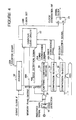
- the comparison registers 14 and 18 are respectively set with reference numbers which fulfil such a relation that the set value of the comparison register 18 is less than the set value of the comparison register 14.
- the comparison register 14 is set with a basic count number of the counter 12, namely, a maximum count value of the counter 12. Therefore, the set value of the comparison register 14 determines one period of the serial clock generated.
- the clock set signal 22B is generated by the third coincidence signal 20A outputted from the capture/comparison register 20.
- the clock set signal 22B is generated by the first coincidence signal 14A outputted from the comparison register 14, regardless of the content of the memory flag 26.
- the capture/comparison register 20 responds to the edge detection signal 10A from the edge detector 10, so as to capture and store the count value of the counter 12.
- the edge detection signal 10A is stored in the memory flag 26 of the counter clear circuit 22.
- the memory flag 26 is also cleared so that the output 26A of the memory flag 26 is rendered inactive.
- the capture operation of the capture/comparison register 20 is allowed, again, and the presetting of the low place bit of the memory flag 26 is also allowed.
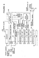
- the edge detection signal 10A is supplied to the capture/comparison register 20 without being masked by the gate circuit 32. Therefore, the capture/comparison register 20 captures and stores the count value of the counter 12. In addition, the edge detection signal 10A is stored in the memory flag 26 of the counter clear circuit 22.
- the counter clear circuit 22 After the counter 12 starts its count operation from “0" again, when the count value of the counter 12 becomes consistent with the stored count value, for example "1" of the capture/comparison register 20, the third coincidence signal 20A is generated by the capture/comparison register 20. At this time, since both the output of the memory flag 26 and the output 38A of the area detection circuit 38 have been already rendered active, the counter clear circuit 22 generates the clock set signal 22B so as to set the clock generation flipflop 24. At the next count timing, the counter clear signal 22A is generated. Therefore, the counter 12 is cleared or returned to "0", and continues its count operation from "0", again.
- the capture/comparison register 20 receives the edge detection signal 10A from the edge detector 10 without being masked by the gate circuit 32, so as to capture and store the count value of the counter 12.
- the edge detection signal 10A is stored in the memory flag 26 of the counter clear circuit 22.
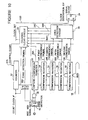
- the count clock ⁇ has a frequency 16 times of the serial transfer rate.
- the edge detection signal 10A is supplied to the capture/comparison register 20. Therefore, the capture/comparison register 20 captures and stores the count value of the counter 12.
- the edge detection signal 10A is stored in the memory flag 46 of the counter clear circuit 22. However, since the output of the memory flag 46 is rendered active only when two active edge detection signals are stored continuously, the output of the memory flag 46 is still "0" at this time.
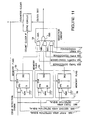
- the clock set signal 22B is applied to the synchronous circuit 30, which is the same as that of the first embodiment and which receives the count clock ⁇ . Therefore, this synchronous circuit 30 will not be explained here.
- the counter clear circuit 22 After the counter 12 starts its count operation from “0" again, when the count value of the counter 12 becomes consistent with the set count value, for example "3" of the fourth comparison register 34, the fourth coincidence signal 34A is generated. At this time, since both the output of the second memory flag 54 and the second area detection signal 38B have been already rendered active, the counter clear circuit 22 generates the clock set signal 22B so as to set the clock generation flipflop 24. At the next count timing, the counter clear signal 22A is generated. Therefore, the counter 12 is cleared to "0", and continues its count operation from “0", again.
Landscapes
- Engineering & Computer Science (AREA)
- Computer Networks & Wireless Communication (AREA)
- Signal Processing (AREA)
- Synchronisation In Digital Transmission Systems (AREA)
Applications Claiming Priority (2)
| Application Number | Priority Date | Filing Date | Title |
|---|---|---|---|
| JP298512/88 | 1988-11-25 | ||
| JP29851288 | 1988-11-25 |
Publications (3)
| Publication Number | Publication Date |
|---|---|
| EP0370528A2 true EP0370528A2 (de) | 1990-05-30 |
| EP0370528A3 EP0370528A3 (de) | 1992-01-15 |
| EP0370528B1 EP0370528B1 (de) | 1995-03-01 |
Family
ID=17860681
Family Applications (1)
| Application Number | Title | Priority Date | Filing Date |
|---|---|---|---|
| EP89121853A Expired - Lifetime EP0370528B1 (de) | 1988-11-25 | 1989-11-27 | Schaltungsanordnung zum Erzeugen eines seriellen Taktsignals |
Country Status (3)
| Country | Link |
|---|---|
| US (1) | US4989223A (de) |
| EP (1) | EP0370528B1 (de) |
| DE (1) | DE68921429T2 (de) |
Cited By (3)
| Publication number | Priority date | Publication date | Assignee | Title |
|---|---|---|---|---|
| EP0588656A3 (en) * | 1992-09-18 | 1994-06-01 | Sony Corp | Digital pll circuit having signal edge position measurement |
| EP0498450A3 (en) * | 1991-02-07 | 1994-06-01 | Nec Corp | Serial clock generating circuit |
| EP1811714A1 (de) * | 2006-01-23 | 2007-07-25 | Micronas GmbH | Integrierte Schaltung für eine asynchrone, serielle Datenübertragung mit einem Billängen Zähler |
Families Citing this family (19)
| Publication number | Priority date | Publication date | Assignee | Title |
|---|---|---|---|---|
| JP2787725B2 (ja) * | 1990-02-14 | 1998-08-20 | 第一電子工業株式会社 | データ・クロックのタイミング合わせ回路 |
| US5223742A (en) * | 1991-08-14 | 1993-06-29 | Schumacher Mark E | Circuit and method for monitoring a pulse width modulated waveform |
| US5293628A (en) * | 1991-11-04 | 1994-03-08 | Motorola, Inc. | Data processing system which generates a waveform with improved pulse width resolution |
| JPH05265943A (ja) * | 1992-03-17 | 1993-10-15 | Nec Corp | シリアルデータ転送装置 |
| JP2773546B2 (ja) * | 1992-05-07 | 1998-07-09 | 日本電気株式会社 | パルス発生回路 |
| US5371772A (en) * | 1993-09-14 | 1994-12-06 | Intel Corporation | Programmable divider exhibiting a 50/50 duty cycle |
| JPH07334450A (ja) * | 1994-06-10 | 1995-12-22 | Mitsubishi Denki Semiconductor Software Kk | インタフェイス装置 |
| JP2707981B2 (ja) * | 1994-10-21 | 1998-02-04 | 株式会社デンソー | 通信制御装置 |
| US5818847A (en) * | 1996-06-06 | 1998-10-06 | Sun Microsystems, Inc. | System and method for providing real time values in digital data processing system |
| JP3815826B2 (ja) * | 1996-09-26 | 2006-08-30 | 富士通株式会社 | デジタル信号処理装置 |
| JPH11265313A (ja) * | 1998-03-18 | 1999-09-28 | Hitachi Ltd | 記憶装置 |
| US6711226B1 (en) * | 2000-05-12 | 2004-03-23 | Cypress Semiconductor Corp. | Linearized digital phase-locked loop |
| JP3956768B2 (ja) * | 2002-05-14 | 2007-08-08 | ソニー株式会社 | クロック発生回路 |
| JP3998532B2 (ja) * | 2002-08-07 | 2007-10-31 | 株式会社ルネサステクノロジ | データ転送装置 |
| US7664214B2 (en) * | 2002-09-24 | 2010-02-16 | Standard Microsystems Corporation | System and method for transferring data among transceivers substantially void of data dependent jitter |
| US7171576B2 (en) * | 2003-04-09 | 2007-01-30 | International Business Machines Corporation | Method, apparatus and program storage device for providing clocks to multiple frequency domains using a single input clock of variable frequency |
| US7826581B1 (en) | 2004-10-05 | 2010-11-02 | Cypress Semiconductor Corporation | Linearized digital phase-locked loop method for maintaining end of packet time linearity |
| KR102285789B1 (ko) | 2014-07-01 | 2021-08-04 | 삼성전자 주식회사 | 외장 저장 장치, 및 이의 기준 주파수를 설정하는 방법 |
| US10340904B2 (en) | 2016-06-28 | 2019-07-02 | Altera Corporation | Method and apparatus for phase-aligned 2X frequency clock generation |
Family Cites Families (6)
| Publication number | Priority date | Publication date | Assignee | Title |
|---|---|---|---|---|
| US3594551A (en) * | 1966-11-29 | 1971-07-20 | Electronic Communications | High speed digital counter |
| US4101761A (en) * | 1976-11-26 | 1978-07-18 | Pacific Western Systems | Timing pulse generator |
| US4280099A (en) * | 1979-11-09 | 1981-07-21 | Sperry Corporation | Digital timing recovery system |
| US4873624A (en) * | 1983-11-04 | 1989-10-10 | Motorola, Inc. | Output compare system and method for a data processor |
| US4628269A (en) * | 1984-05-23 | 1986-12-09 | Motorola, Inc. | Pulse detector for missing or extra pulses |
| US4856029A (en) * | 1988-10-11 | 1989-08-08 | Eastman Kodak Company | Technique for processing a digital signal having zero overhead sync |
-
1989
- 1989-11-27 EP EP89121853A patent/EP0370528B1/de not_active Expired - Lifetime
- 1989-11-27 DE DE68921429T patent/DE68921429T2/de not_active Expired - Fee Related
- 1989-11-27 US US07/441,112 patent/US4989223A/en not_active Expired - Fee Related
Cited By (5)
| Publication number | Priority date | Publication date | Assignee | Title |
|---|---|---|---|---|
| EP0498450A3 (en) * | 1991-02-07 | 1994-06-01 | Nec Corp | Serial clock generating circuit |
| EP0588656A3 (en) * | 1992-09-18 | 1994-06-01 | Sony Corp | Digital pll circuit having signal edge position measurement |
| US5428648A (en) * | 1992-09-18 | 1995-06-27 | Sony Corporation | Digital PLL circuit having signal edge position measurement |
| EP1811714A1 (de) * | 2006-01-23 | 2007-07-25 | Micronas GmbH | Integrierte Schaltung für eine asynchrone, serielle Datenübertragung mit einem Billängen Zähler |
| US8275083B2 (en) | 2006-01-23 | 2012-09-25 | Micronas Gmbh | Integrated circuit for an asynchronous serial data transfer with a bit length counter |
Also Published As
| Publication number | Publication date |
|---|---|
| EP0370528B1 (de) | 1995-03-01 |
| EP0370528A3 (de) | 1992-01-15 |
| DE68921429D1 (de) | 1995-04-06 |
| US4989223A (en) | 1991-01-29 |
| DE68921429T2 (de) | 1995-11-09 |
Similar Documents
| Publication | Publication Date | Title |
|---|---|---|
| EP0370528B1 (de) | Schaltungsanordnung zum Erzeugen eines seriellen Taktsignals | |
| US6275546B1 (en) | Glitchless clock switch circuit | |
| US6954506B2 (en) | Clock signal recovery circuit used in receiver of universal serial bus and method of recovering clock signal | |
| EP0398329B1 (de) | Demodulatorschaltung für Spreizspektrumsignal | |
| US6249188B1 (en) | Error-suppressing phase comparator | |
| US4466110A (en) | Artificial sync signal adding circuit | |
| EP0214676B1 (de) | Taktsignal-Regeneratoranordnung | |
| JP2765245B2 (ja) | シリアルクロック発生回路 | |
| US6339833B1 (en) | Automatic recovery from clock signal loss | |
| US6137851A (en) | System and method for synchronizing a signal with respect to another signal | |
| US5418496A (en) | Serial data clock recovery circuit using dual oscillator circuit | |
| US6597627B2 (en) | Clock switching circuitry for avoiding conflict of data handling occuring in a memory | |
| US5656958A (en) | Frequency synthesizing device | |
| US7809973B2 (en) | Spread spectrum clock for USB | |
| JPS62168415A (ja) | ラツチ間伝送方式 | |
| JPH02216513A (ja) | シリアルクロック発生回路 | |
| JP2798918B2 (ja) | パルス幅変調回路 | |
| JPS62202624A (ja) | 高速デ−タ受信回路方式 | |
| JPS6343930B2 (de) | ||
| JP2681922B2 (ja) | ビット同期装置 | |
| JP2522259B2 (ja) | デイジタル型位相同期方法 | |
| JP2930083B2 (ja) | パラレル/シリアル変換回路 | |
| JPH0637743A (ja) | 直列データ受信装置 | |
| JPH08331189A (ja) | クロック位相同期回路 | |
| JPS61180357A (ja) | デ−タラツチ回路 |
Legal Events
| Date | Code | Title | Description |
|---|---|---|---|
| PUAI | Public reference made under article 153(3) epc to a published international application that has entered the european phase |
Free format text: ORIGINAL CODE: 0009012 |
|
| AK | Designated contracting states |
Kind code of ref document: A2 Designated state(s): DE FR GB |
|
| 17P | Request for examination filed |
Effective date: 19900620 |
|
| PUAL | Search report despatched |
Free format text: ORIGINAL CODE: 0009013 |
|
| AK | Designated contracting states |
Kind code of ref document: A3 Designated state(s): DE FR GB |
|
| 17Q | First examination report despatched |
Effective date: 19940107 |
|
| GRAA | (expected) grant |
Free format text: ORIGINAL CODE: 0009210 |
|
| AK | Designated contracting states |
Kind code of ref document: B1 Designated state(s): DE FR GB |
|
| ET | Fr: translation filed | ||
| REF | Corresponds to: |
Ref document number: 68921429 Country of ref document: DE Date of ref document: 19950406 |
|
| PGFP | Annual fee paid to national office [announced via postgrant information from national office to epo] |
Ref country code: FR Payment date: 19951116 Year of fee payment: 7 |
|
| PGFP | Annual fee paid to national office [announced via postgrant information from national office to epo] |
Ref country code: DE Payment date: 19951120 Year of fee payment: 7 |
|
| PGFP | Annual fee paid to national office [announced via postgrant information from national office to epo] |
Ref country code: GB Payment date: 19951123 Year of fee payment: 7 |
|
| PLBE | No opposition filed within time limit |
Free format text: ORIGINAL CODE: 0009261 |
|
| STAA | Information on the status of an ep patent application or granted ep patent |
Free format text: STATUS: NO OPPOSITION FILED WITHIN TIME LIMIT |
|
| 26N | No opposition filed | ||
| PG25 | Lapsed in a contracting state [announced via postgrant information from national office to epo] |
Ref country code: GB Effective date: 19961127 |
|
| GBPC | Gb: european patent ceased through non-payment of renewal fee |
Effective date: 19961127 |
|
| PG25 | Lapsed in a contracting state [announced via postgrant information from national office to epo] |
Ref country code: FR Effective date: 19970731 |
|
| PG25 | Lapsed in a contracting state [announced via postgrant information from national office to epo] |
Ref country code: DE Effective date: 19970801 |
|
| REG | Reference to a national code |
Ref country code: FR Ref legal event code: ST |