EP0370928A2 - Gerät, Verfahren und Datenstruktur zur Gültigkeitserklärung vom Kern-Datenbus - Google Patents
Gerät, Verfahren und Datenstruktur zur Gültigkeitserklärung vom Kern-Datenbus Download PDFInfo
- Publication number
- EP0370928A2 EP0370928A2 EP89420461A EP89420461A EP0370928A2 EP 0370928 A2 EP0370928 A2 EP 0370928A2 EP 89420461 A EP89420461 A EP 89420461A EP 89420461 A EP89420461 A EP 89420461A EP 0370928 A2 EP0370928 A2 EP 0370928A2
- Authority
- EP
- European Patent Office
- Prior art keywords
- data bus
- bit pattern
- lines
- bit
- bus
- Prior art date
- Legal status (The legal status is an assumption and is not a legal conclusion. Google has not performed a legal analysis and makes no representation as to the accuracy of the status listed.)
- Withdrawn
Links
Images


Classifications
-
- G—PHYSICS
- G06—COMPUTING OR CALCULATING; COUNTING
- G06F—ELECTRIC DIGITAL DATA PROCESSING
- G06F11/00—Error detection; Error correction; Monitoring
- G06F11/22—Detection or location of defective computer hardware by testing during standby operation or during idle time, e.g. start-up testing
- G06F11/26—Functional testing
- G06F11/261—Functional testing by simulating additional hardware, e.g. fault simulation
-
- G—PHYSICS
- G06—COMPUTING OR CALCULATING; COUNTING
- G06F—ELECTRIC DIGITAL DATA PROCESSING
- G06F11/00—Error detection; Error correction; Monitoring
- G06F11/22—Detection or location of defective computer hardware by testing during standby operation or during idle time, e.g. start-up testing
- G06F11/2205—Detection or location of defective computer hardware by testing during standby operation or during idle time, e.g. start-up testing using arrangements specific to the hardware being tested
- G06F11/221—Detection or location of defective computer hardware by testing during standby operation or during idle time, e.g. start-up testing using arrangements specific to the hardware being tested to test buses, lines or interfaces, e.g. stuck-at or open line faults
Definitions
- the present invention relates generally to the testing and troubleshooting of microprocessor-based electronic systems and more particularly to testing and troubleshooting of the kernel of microprocessor-based electronic systems using a memory emulation technique.
- the kernel of such a system is well-understood in the art to refer to the microprocessor ( ⁇ P), itself, and the associated elements with which it is necessary for the microprocessor to correctly interact to function correctly, specifically the memory, clock, address bus and data bus.
- ⁇ P microprocessor
- So-called emulative testers in which an element of the kernel is emulated by the testing apparatus have become popular for functional testing because they enable detailed diagnostics of the kernel even where the kernel is not even minimally operative.
- One type of emulative tester is a microprocessor emulator, exemplified by the tester described in U. S. patent 4,455,654, issued to K. S. Bhaskar et al and assigned to the John Fluke Mfg. Co., Inc.; In that system, connection is made to the UUT by removing the UUT ⁇ P and connecting the test system through the ⁇ P socket of the UUT.
- ROM or memory emulator
- ROM emulation is deemed desireable since the ROM is in direct communication with the UUT data and address buses and the pin configurations of ROM sockets are relatively simple.
- ROM emulators are well known for use in software design and operational verification of the ⁇ P but have only recently been used for fault detection and diagnosis because no sync signal is typically available to synchronize the test equipment with the test results it receives. A solution to this problem is disclosed in U. S. Patent Application 07/158,223, of M. H.
- test system comprises a ⁇ P-based mainframe and an interface pod which also includes a ⁇ P-based system which is connected to both the ⁇ P and the memory socket of the UUT.
- the interface pod includes special logic circuitry connected to the UUT ⁇ P to provide a fine resolution sync signal pulse during a bus cycle of interest in order to provide full troubleshooting fault isolation that is as effective as that provided by prior art ⁇ P emulation since the high resolution sync pulse derived from the ⁇ P can be used to isolate and evaluate signals monitored from the address and data buses at the memory socket with the same facility as they could be from ⁇ P connections.
- ROM emulation may be generalized to memory emulation (e.g. the emulation of any memory or portion of memory) since the trend in ⁇ P-based systems is to increase RAM while reducing ROM and possibly eliminating ROM altogether by substituting RAM. Therefore test systems must be adequately generalized to test systems not yet produced but, nonetheless, foreseeable in light of current trends in electronic microprocessor-based system architecture.
- the term “verification”, as used herein indicates the ascertaining of at least a minimum level of functionality which is sufficient to allow a subsequent procedure to be conducted.
- the term “validation” indicates that if no fault is found, the entire structure validated may be considered fully funtional.
- the term “test” is used to indicate a procedure where all existing faults will be found, but not necessarily isolated or identified.
- Diagnosis indicates that all faults are found and identified.
- the reason for performing verification rather than testing of the data bus is to reduce the time necessary to perform complete diagnosis of the kernel of the UUT.
- the single slowest element of the test is the test of the upper data bus which has required manual probing by the operator of the test system for data bus testing and diagnosis.
- signals which reflect the condition of the kernel are collected from the address by the emulation memory. Therefore, unless the data bus functions correctly, such signals will be ambiguous as to whether a fault found exists on the data bus or the address bus.
- Testing of the address bus requires no probing and takes little time and if no fault is found, both the data bus and the address bus will be found to be fully functional.
- the invention is directed to an apparatus for testing and validation of the data bus of the kernel of a microprocessor-based system by memory emulation, including a method for validation of the data bus.
- a load operation is performed to force onto a first plurality of lines of the data bus a first bit pattern containing a number of bits equal to one-half the number of lines in the data bus.
- a load operation is performed of a second bit pattern which is the complement of said first bit pattern over a second plurality of bus lines constituted by the remainder of the data bus lines.
- the first and second bit patterns are compared and a signal is generated if the second bit pattern is not the complement of the first bit pattern.
- a load operation of a third bit pattern containing a number of bits equal to one-half the number of lines in the data bus over a third plurality of lines in the data bus is performed and as is a load operation of a fourth bit pattern which is not the complement of the third bit pattern over a fourth plurality of bus lines constituted by the remainder of the data bus lines.
- said third and fourth bit patterns are compared and a signal is generated if the fourth bit pattern is not the complement of the third bit pattern.
- the first and second pattern could be simultaneously loaded, perhaps in a single operation, as may be convenient, as can the third and fourth patterns. However, it may not be convenient to do so if the second and fourth patterns are respectively developed from the first and third patterns rather than stored.
- the data bus may be entirely validated and the overall test procedure may be greatly expedited since the validation routine obviate the need for probing of the data bus lines if no fault is reported.
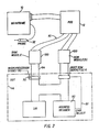
- test apparatus connected to a UUT 14 includes a mainframe processor 10, arranged in a compact housing and including a keyboard 20, probe 32 and display 22, an interface pod 12, a sync module 150 including a sync module adapter 150 and at least one memory module 100 (two being illustrated) depending upon the memory configuration of the UUT 14.
- the memory module(s) connect to the UUT by a multi- conductor cable 92 and a plug corresponding to the UUT memory socket 72.
- Figure 2 schematically illustrates the interconnection of the system shown in figure 1, showing the preferred arrangement of the apparatus in a plurality of housings.
- the particular articulation of the elements of the system while being preferably as shown for the convenience of the operator could be packaged in more or fewer elements than shown.
- the pod could be entirely included within the same housing as the mainframe.
- the sync module is connected to the ⁇ P which is left in place in the UUT circuit.
- the validation routine of this invention compises a stimulus routine including passing a bit pattern which is half as wide as the data bus, or the portion of the data bus to be validated, over, say, the low order lines of the data bus, or portion thereof, and passing the same bit pattern or complement of that bit pattern over the high order lines of the data bus, or portion, and evaluating the bit patterns received on the respective high and low order lines to determine whether the bit patterns are or are not complements of each other. Since the patterns are both true and complemented patterns, differing results of the evaluation are sufficient to validate the entire width of the data bus.
- the testing system includes a plurality of novel procedures including a bus test primitive, a data stimulus primitive and an address stimulus primitive, which will be individually summarized below.
- Each of these primitives has utility for testing a particular portion of the kernel of a ⁇ P-based system and when utilized in a sequence according to the invention permit a higher degree of automated testing and diagnostics at higher speed and with greater operator convenience than has heretofore been available.
- the bus test primitive is executed by a program in the mainframe of the test apparatus.
- the main function of the bus test primitive is to determine if the ⁇ P is able to perform basic read and write operations in the kernel and can consist of as little as a single read and write. If successful, it will be known that the ⁇ P is at least capable of accessing the memory, in this case, the emulation memory, receiving a bit pattern over the data bus and placing that bit pattern on the address bus where it can be received and monitored by the pod. Since the testing apparatus performs diagnostics of the data and address buses by the development of signatures, however, in the preferred embodiment, the bus test primitive is implemented as a program which is designed to exercise the portion of the data and address buses which correspond to the boot memory.
- bus test primitive is not exhaustive of the lines comprising the data and address buses or even of the combinations of bits which can be placed on those lines or portion of those lines and can thus function rapidly as a go/no go test.
- the data stimulus primitive is implemented at a lower level of operability of the ⁇ P than the bus test primitive, specifically by repeatedly resetting the ⁇ P; which function will have been tested prior to execution of the bus test primitive.
- the ⁇ P accesses the first location in the boot memory and retrieves the bit pattern stored there.
- the data stimulus is not a program but is executed by altering the bit pattern in the first location of the boot memory for each reset. It is significant to note that this function is common to both the so-called vectored reset and execute-on-reset types of microprocessors. With either type of ⁇ P, the bit pattern retrieved from memory will be communicated over the data bus and will appear on the address bus.
- a sync pulse is generated by the ⁇ P during the initial reading of the first location of the boot memory which is captured by the sync module, communicated to the pod and used to evaluate signals appearing on the data bus, either by probing or non-probing tests to collect data bus line signatures.
- the latter is done by a procedure similar to the bus test using an exhaustive data stimulus sequence of bit patterns while monitoring the chip select line.
- the data stimulus sequence is exhaustive in the sense that it consists of a series of essentially arbitrary patterns which are, nevertheless, chosen such that a unique signature will be generated on each line of the data bus.
- the chip select line (which is a logic function of the high-order bits on the address bus) will reflect an error only if one or more of the high-order bits is non-zero as is expected when cycling through boot space locations and the go/no go test will be passed even if one or more of the high order bus lines are tied to ground.
- the presence or absence of a chip select signal as expected while performing the data stimulus sequence will reflect whether or not one of the high order lines is latched (e.g. shorted to ground). If this test is passed, only tied line defects, where a line of the data bus is tied to another data bus line will remain. This can be later diagnosed by probing.
- it is preferable to validate the data bus at this point whereby, if no faults are reported by the validation routine, the data bus will be known to be fully, functional.
- testing of the address bus may be conducted using the same stimulus sequence as for the data stimulus primitive. However, this is done by conducting a programmed sequence of read/write instructions using these bit patterns and collecting signatures either with a probe, or preferably, in an analysis memory from which latched or tied lines may be deduced. As pointed out above, an exhaustive test of the address lines may be conducted using only the limited number of bit patterns in the stimulus sequence. Once the address bus lines have thus been fully diagnosed, full diagnosis of the data lines will be possible since any defect appearing on the databus lines will also be reflected on the address bus lines. Since the address bus lines have been fully diagnosed, any fault noted will be isolated to a particular bus.
- the program for performing the address stimulus primitive can be a single instruction.
- the address stimulus primitive typically requires no instructions at all; the desired bit pattern is merely placed into the emulation memory at the reset vector location.
- an emulation memory is electrically substituted for the memory of the unit to be tested and a sync module is connected to timing information and forcing pins of the ⁇ P by conductors 140 ( Figure 3).
- a sync module is connected to timing information and forcing pins of the ⁇ P by conductors 140 ( Figure 3).
- a reset overdrive check is performed to determine if the pod can, in fact, initiate a reset of the ⁇ P and is monitored by the sync module to determine if the reset line first goes active and then inactive. The actual reset of the ⁇ P is not checked in this step but only that a signal which should be capable of doing so is present at the appropriate pin of the ⁇ P.
- the sync module captures the clock signal of the ⁇ P which is evaluated. If the ⁇ P clock signal is not received by the pod, additional checks are made of the clock to determine if it is slow or shorted and for unexpected values of the signals on the forcing lines.
- the ⁇ P reset is now done by overdriving the reset line and looking for a chip select signal on the chip select line corresponding to the boot memory location from address decoder 80. If successful, the ⁇ P will again be reset for the purpose of checking for the correct signal on the low order lines of the address bus to access the first location of the boot memory. This procedure will now have verified sufficient functionality of the kernel to proceed with the sequence of the bus test, and the sequence of data and address stimulus primitives as outlined above.
- the data bus validation routine comprises the accessing of a bit pattern from the emulation memory and placing that pattern on a portion of the data bus (401). Then the complement of the bit pattern is preferably produced by the ⁇ P from the bit pattern (402) and placed on another portion of the data bus (403). A comparison of the two portions of the dataq bus are then compared (404) and a signal is generated if the two bit patterns are not complements of each other. This result can be immediately reported but is preferably collected (410) over a sequence of bit patterns. These steps are preferably repeated through a predetermined sequence of patterns. This sequence need not be conducted in a single series of operations but can be interrupted or interleaved with the similar series of steps 406 - 409.
- the process of validation of the data bus is continued by placing a bit pattern, preferably from a second sequence of bit patterns, on a portion of the data bus (406). In this sequence, as distinct from the previous sequences, the same bit pattern is placed no a second portion of the data bus (407). Comparison is again made (408) and the result of the comparison is collected (411). These steps ar then preferably repeated through the second sequence of patterns (409).
- the collected comparison results 410 and 411 are evaluated and the data bus in considered to be validated if the first series reports all complements and the second series reports none.
- conductors 140 are connected to the reset line and other lines on which signals reflecting the operational state (status pins) of the UUT ⁇ P will appear. For example, on the 80386 processor, these lines will be the HOLD, HLDA (hold acknowledge), ADS , READY , CLK2, and RESET lines. These signals will be received by buffers 152 over lines 140 and transmitted to the pod over cable 90 as inputs to bus cycle state machine 200. Bus cycle state machine 200 will perform a logical operation on these signals, under control of the mainframe 10, to develop a control signal for controlling sync pulse generation state machine 202 which generates a sync signal in response thereto. This sync signal is sent to mainframe 10 which generates control signals therefrom which are returned to various parts of the pod as illustrated, notably the analyzer RAM 62.
- the mechanism for analyzing the address trace is the same one that is used for analyzing the trace from the Bus Test primitive. This is more fully described in the disclosure "AUTOMATIC VERIFICATION OF KERNEL CIRDUITRY BASED ON ANALYSIS OF MEMORY ACCESSES by J. Polstra and assigned to the assignee of this application, which is hereby incorporated by reference.
- bit patterns are used in each of two sequences.
- One sequence will force each of the bit patterns and its complement onto the full width of the data bus.
- These patterns (in HEX notation are preferably
- These patterns are chosen to insure that all data line faults will be detected by at least one pattern. Faults which will be detected are, for example, lines stuck high or low and lines tied to other lines. Since the data bus will be validated only if all of the one sequence of patterns are reported as complementary high and low order bit pattern and none of the other sequence are reported as complementary high and low order bit patterns, it is also assured that no data bus line fault can be reported incorrectly as a pass.
- This validation procedure is equally applicable to processors with 4 bit, 8 bit, 16 bit, 32 bit or any other width of data bus.
- the listing shows the binary levels that will (in a good UUT) be present on the 32 lines of the data bus during each step of the program. As shown, the listing represents a UUT which actually utilizes all 32 data lines of the 80386. However, the test is, as noted above; effective for UUTs which utilize fewer data lines.
- the "Label” column gives an option symbolic name for the address of the current instruction. This is common practice in assembly language programming.
- the "Opcode” column gives the symbolic name for an 80386 machine instruction.
- the "Operands” column lists the operands (parameters) which more fully specify the precise action to be taken by the microprocessor.
- Each instruction fetch transfers a full 32 bits of information across the data bus.
- Such a transfer may contain one or more full or partial 80386 instructions.
- An instruction may also be split across two 32-bit transfers. This can be seen with the "xor ax,YYYYYYYYYYYYYYYYYYYYYYYYYY" instruction, which begins in one set of 32 bits, but ends in another set.
- a step-by-step description of the program is as follows:
- This instruction causes the processor to perform an infinite loop at the failure address, namely FFFFF800.
- the pod gathers a trace of the UUT's address references, using the Address RAM (ARAM). It then analyzes the sequences of address. If it sees a series of sequential accesses, followed by a jump back to the "success" address, then the pod knows that the test passed. If it sees anything else (usually, a jump to the "failure” address) the pod knows that the test failed.
- ARAM Address RAM
Landscapes
- Engineering & Computer Science (AREA)
- General Engineering & Computer Science (AREA)
- Theoretical Computer Science (AREA)
- Computer Hardware Design (AREA)
- Quality & Reliability (AREA)
- Physics & Mathematics (AREA)
- General Physics & Mathematics (AREA)
- Test And Diagnosis Of Digital Computers (AREA)
Applications Claiming Priority (2)
| Application Number | Priority Date | Filing Date | Title |
|---|---|---|---|
| US07/275,185 US4958347A (en) | 1988-11-23 | 1988-11-23 | Apparatus, method and data structure for validation of kernel data bus |
| US275185 | 1988-11-23 |
Publications (2)
| Publication Number | Publication Date |
|---|---|
| EP0370928A2 true EP0370928A2 (de) | 1990-05-30 |
| EP0370928A3 EP0370928A3 (de) | 1992-01-15 |
Family
ID=23051237
Family Applications (1)
| Application Number | Title | Priority Date | Filing Date |
|---|---|---|---|
| EP19890420461 Withdrawn EP0370928A3 (de) | 1988-11-23 | 1989-11-22 | Gerät, Verfahren und Datenstruktur zur Gültigkeitserklärung vom Kern-Datenbus |
Country Status (4)
| Country | Link |
|---|---|
| US (1) | US4958347A (de) |
| EP (1) | EP0370928A3 (de) |
| JP (1) | JPH0610791B2 (de) |
| CN (1) | CN1043019A (de) |
Cited By (1)
| Publication number | Priority date | Publication date | Assignee | Title |
|---|---|---|---|---|
| WO1996036885A1 (en) * | 1995-05-15 | 1996-11-21 | Advanced Micro Devices, Inc. | Bus connectivity verification technique |
Families Citing this family (9)
| Publication number | Priority date | Publication date | Assignee | Title |
|---|---|---|---|---|
| US5204864A (en) * | 1990-08-16 | 1993-04-20 | Westinghouse Electric Corp. | Multiprocessor bus debugger |
| US5247522A (en) * | 1990-11-27 | 1993-09-21 | Digital Equipment Corporation | Fault tolerant bus |
| US5164295A (en) * | 1991-03-06 | 1992-11-17 | The Upjohn Company | Method for identifying amyloid protein-extracellular matrix protein affinity altering compounds |
| US5546408A (en) * | 1994-06-09 | 1996-08-13 | International Business Machines Corporation | Hierarchical pattern faults for describing logic circuit failure mechanisms |
| KR0149891B1 (ko) * | 1994-12-22 | 1999-05-15 | 윤종용 | 버스상태분석기 및 그 내부버스시험방법 |
| US20010039564A1 (en) * | 1997-10-20 | 2001-11-08 | Victor Hahn | Log on personal computer |
| US6970816B1 (en) | 2000-08-14 | 2005-11-29 | International Business Machines Corporation | Method and system for efficiently generating parameterized bus transactions |
| US7036054B2 (en) * | 2003-07-02 | 2006-04-25 | Nokia Corporation | Memory bus checking procedure |
| CN100446129C (zh) * | 2006-09-07 | 2008-12-24 | 华为技术有限公司 | 一种内存故障测试的方法及系统 |
Family Cites Families (19)
| Publication number | Priority date | Publication date | Assignee | Title |
|---|---|---|---|---|
| US3289160A (en) * | 1963-12-23 | 1966-11-29 | Ibm | Means for comparing digital values |
| US4055801A (en) * | 1970-08-18 | 1977-10-25 | Pike Harold L | Automatic electronic test equipment and method |
| US4108358A (en) * | 1977-03-22 | 1978-08-22 | The Bendix Corporation | Portable circuit tester |
| US4139818A (en) * | 1977-09-30 | 1979-02-13 | Burroughs Corporation | Circuit means for collecting operational errors in IC chips and for identifying and storing the locations thereof |
| US4192451A (en) * | 1978-05-30 | 1980-03-11 | Tektronix, Inc. | Digital diagnostic system employing signature analysis |
| US4402055A (en) * | 1981-01-27 | 1983-08-30 | Westinghouse Electric Corp. | Automatic test system utilizing interchangeable test devices |
| FR2531230A1 (fr) * | 1982-07-27 | 1984-02-03 | Rank Xerox Sa | Ensemble destine au test automatique centralise de circuits imprimes et procede de test de circuits a microprocesseur faisant application de cet ensemble |
| FR2532771B1 (fr) * | 1982-09-08 | 1988-05-13 | Service Sa | Procede et dispositif pour tester statiquement l'ensemble des connexions et des circuits integres peripheriques d'un microprocesseur |
| DE3241412A1 (de) * | 1982-11-09 | 1984-05-10 | Siemens AG, 1000 Berlin und 8000 München | Vorrichtung zum testen eines hochintegrierten mikroprogramm-gesteuerten elektronischen bauteiles |
| US4622669A (en) * | 1983-02-07 | 1986-11-11 | Motorola, Inc. | Test module for asynchronous bus |
| US4641207A (en) * | 1983-03-22 | 1987-02-03 | Green George D | Diagnostic device and method for examining the operation of a disk drive |
| US4550406A (en) * | 1983-06-14 | 1985-10-29 | Everett/Charles Test Equipment, Inc. | Automatic test program list generation using programmed digital computer |
| US4641348A (en) * | 1983-11-09 | 1987-02-03 | Hewlett-Packard Company | Timing or logic state analyzer with automatic qualified inferential marking and post processing of captured trace data |
| US4656632A (en) * | 1983-11-25 | 1987-04-07 | Giordano Associates, Inc. | System for automatic testing of circuits and systems |
| US4757503A (en) * | 1985-01-18 | 1988-07-12 | The University Of Michigan | Self-testing dynamic ram |
| US4691316A (en) * | 1985-02-14 | 1987-09-01 | Support Technologies, Inc. | ROM emulator for diagnostic tester |
| ATE53261T1 (de) * | 1985-03-26 | 1990-06-15 | Siemens Ag | Verfahren zum betreiben eines halbleiterspeichers mit integrierter paralleltestmoeglichkeit und auswerteschaltung zur durchfuehrung des verfahrens. |
| US4687988A (en) * | 1985-06-24 | 1987-08-18 | International Business Machines Corporation | Weighted random pattern testing apparatus and method |
| US4847838A (en) * | 1987-06-22 | 1989-07-11 | Ag Communication Systems Corporation | Circuit for testing the bus structure of a printed wiring card |
-
1988
- 1988-11-23 US US07/275,185 patent/US4958347A/en not_active Expired - Fee Related
-
1989
- 1989-11-21 CN CN89108771.0A patent/CN1043019A/zh active Pending
- 1989-11-22 JP JP1304517A patent/JPH0610791B2/ja not_active Expired - Lifetime
- 1989-11-22 EP EP19890420461 patent/EP0370928A3/de not_active Withdrawn
Cited By (2)
| Publication number | Priority date | Publication date | Assignee | Title |
|---|---|---|---|---|
| WO1996036885A1 (en) * | 1995-05-15 | 1996-11-21 | Advanced Micro Devices, Inc. | Bus connectivity verification technique |
| US5602989A (en) * | 1995-05-15 | 1997-02-11 | Advanced Micro Devices Inc. | Bus connectivity verification technique |
Also Published As
| Publication number | Publication date |
|---|---|
| US4958347A (en) | 1990-09-18 |
| JPH0610791B2 (ja) | 1994-02-09 |
| JPH02201548A (ja) | 1990-08-09 |
| CN1043019A (zh) | 1990-06-13 |
| EP0370928A3 (de) | 1992-01-15 |
Similar Documents
| Publication | Publication Date | Title |
|---|---|---|
| US5136590A (en) | Kernel testing interface and method for automating diagnostics of microprocessor-based systems | |
| US4868822A (en) | Memory emulation method and system for testing and troubleshooting microprocessor-based electronic systems | |
| KR100932562B1 (ko) | 집적 회로 및 이의 테스트 방법 | |
| US6842865B2 (en) | Method and system for testing microprocessor based boards in a manufacturing environment | |
| US4993027A (en) | Method and apparatus for determining microprocessor kernal faults | |
| EP0640920A1 (de) | Abtastpfadsystem und Prüf- und Diagnoseverfahren | |
| JPH0643218A (ja) | 環境エミュレーションによるテスト発生 | |
| US4493078A (en) | Method and apparatus for testing a digital computer | |
| JP3645578B2 (ja) | スマート・メモリの組込み自己検査のための装置と方法 | |
| US4680761A (en) | Self diagnostic Cyclic Analysis Testing System (CATS) for LSI/VLSI | |
| US20040216061A1 (en) | Embeddable method and apparatus for functional pattern testing of repeatable program instruction-driven logic circuits via signal signature generation | |
| US4958347A (en) | Apparatus, method and data structure for validation of kernel data bus | |
| US5068852A (en) | Hardware enhancements for improved performance of memory emulation method | |
| US4989207A (en) | Automatic verification of kernel circuitry based on analysis of memory accesses | |
| US20030053358A1 (en) | Dft technique for avoiding contention/conflict in logic built-in self-test | |
| EP0611036A1 (de) | Verfahren zur automatischen Ermittlung von offenen Schaltkreisen | |
| Sedmark | Boundary-scan: beyond production test | |
| US5293387A (en) | Method for increasing the resolution of a digital fault dictionary | |
| US6718498B2 (en) | Method and apparatus for the real time manipulation of a test vector to access the microprocessor state machine information using the integrated debug trigger | |
| Melocco et al. | A comprehensive approach to assessing and analyzing 1149.1 test logic | |
| EP0370927A2 (de) | Hardwaresteigerungen zur Leistungsverbesserung eines Speicheremulationsverfahrens | |
| Humphrey et al. | Signature analysis for board testing | |
| Mitchell | Lessons learned using boundary scan and built-in test for integration and diagnostic test of the US Navy joint standoff weapon | |
| Reilly et al. | An implementation of microdiagnostics on the ECLIPSE® MV/8000 | |
| Bradshaw | Diagnostics in Computer Controlled Equipment |
Legal Events
| Date | Code | Title | Description |
|---|---|---|---|
| PUAI | Public reference made under article 153(3) epc to a published international application that has entered the european phase |
Free format text: ORIGINAL CODE: 0009012 |
|
| AK | Designated contracting states |
Kind code of ref document: A2 Designated state(s): DE FR GB |
|
| PUAL | Search report despatched |
Free format text: ORIGINAL CODE: 0009013 |
|
| AK | Designated contracting states |
Kind code of ref document: A3 Designated state(s): DE FR GB |
|
| 17P | Request for examination filed |
Effective date: 19920311 |
|
| 17Q | First examination report despatched |
Effective date: 19940209 |
|
| STAA | Information on the status of an ep patent application or granted ep patent |
Free format text: STATUS: THE APPLICATION IS DEEMED TO BE WITHDRAWN |
|
| 18D | Application deemed to be withdrawn |
Effective date: 19940621 |