EP0372476A2 - Dispositif semi-conducteur ayant une capacité parasite réduite et méthode pour sa fabrication - Google Patents
Dispositif semi-conducteur ayant une capacité parasite réduite et méthode pour sa fabrication Download PDFInfo
- Publication number
- EP0372476A2 EP0372476A2 EP89122383A EP89122383A EP0372476A2 EP 0372476 A2 EP0372476 A2 EP 0372476A2 EP 89122383 A EP89122383 A EP 89122383A EP 89122383 A EP89122383 A EP 89122383A EP 0372476 A2 EP0372476 A2 EP 0372476A2
- Authority
- EP
- European Patent Office
- Prior art keywords
- conduction type
- polycrystalline silicon
- layer
- recess
- silicon layer
- Prior art date
- Legal status (The legal status is an assumption and is not a legal conclusion. Google has not performed a legal analysis and makes no representation as to the accuracy of the status listed.)
- Granted
Links
Images

Classifications
-
- H—ELECTRICITY
- H10—SEMICONDUCTOR DEVICES; ELECTRIC SOLID-STATE DEVICES NOT OTHERWISE PROVIDED FOR
- H10D—INORGANIC ELECTRIC SEMICONDUCTOR DEVICES
- H10D10/00—Bipolar junction transistors [BJT]
- H10D10/01—Manufacture or treatment
- H10D10/051—Manufacture or treatment of vertical BJTs
-
- H—ELECTRICITY
- H10—SEMICONDUCTOR DEVICES; ELECTRIC SOLID-STATE DEVICES NOT OTHERWISE PROVIDED FOR
- H10D—INORGANIC ELECTRIC SEMICONDUCTOR DEVICES
- H10D10/00—Bipolar junction transistors [BJT]
- H10D10/40—Vertical BJTs
-
- H—ELECTRICITY
- H10—SEMICONDUCTOR DEVICES; ELECTRIC SOLID-STATE DEVICES NOT OTHERWISE PROVIDED FOR
- H10D—INORGANIC ELECTRIC SEMICONDUCTOR DEVICES
- H10D62/00—Semiconductor bodies, or regions thereof, of devices having potential barriers
- H10D62/10—Shapes, relative sizes or dispositions of the regions of the semiconductor bodies; Shapes of the semiconductor bodies
- H10D62/13—Semiconductor regions connected to electrodes carrying current to be rectified, amplified or switched, e.g. source or drain regions
- H10D62/133—Emitter regions of BJTs
-
- H—ELECTRICITY
- H10—SEMICONDUCTOR DEVICES; ELECTRIC SOLID-STATE DEVICES NOT OTHERWISE PROVIDED FOR
- H10D—INORGANIC ELECTRIC SEMICONDUCTOR DEVICES
- H10D62/00—Semiconductor bodies, or regions thereof, of devices having potential barriers
- H10D62/10—Shapes, relative sizes or dispositions of the regions of the semiconductor bodies; Shapes of the semiconductor bodies
- H10D62/17—Semiconductor regions connected to electrodes not carrying current to be rectified, amplified or switched, e.g. channel regions
- H10D62/177—Base regions of bipolar transistors, e.g. BJTs or IGBTs
-
- H—ELECTRICITY
- H10—SEMICONDUCTOR DEVICES; ELECTRIC SOLID-STATE DEVICES NOT OTHERWISE PROVIDED FOR
- H10D—INORGANIC ELECTRIC SEMICONDUCTOR DEVICES
- H10D64/00—Electrodes of devices having potential barriers
- H10D64/01—Manufacture or treatment
- H10D64/011—Manufacture or treatment of electrodes ohmically coupled to a semiconductor
- H10D64/0111—Manufacture or treatment of electrodes ohmically coupled to a semiconductor to Group IV semiconductors
- H10D64/0113—Manufacture or treatment of electrodes ohmically coupled to a semiconductor to Group IV semiconductors the conductive layers comprising highly doped semiconductor materials, e.g. polysilicon layers or amorphous silicon layers
-
- H—ELECTRICITY
- H10—SEMICONDUCTOR DEVICES; ELECTRIC SOLID-STATE DEVICES NOT OTHERWISE PROVIDED FOR
- H10P—GENERIC PROCESSES OR APPARATUS FOR THE MANUFACTURE OR TREATMENT OF DEVICES COVERED BY CLASS H10
- H10P32/00—Diffusion of dopants within, into or out of wafers, substrates or parts of devices
- H10P32/10—Diffusion of dopants within, into or out of semiconductor bodies or layers
- H10P32/14—Diffusion of dopants within, into or out of semiconductor bodies or layers within a single semiconductor body or layer in a solid phase; between different semiconductor bodies or layers, both in a solid phase
- H10P32/1408—Diffusion of dopants within, into or out of semiconductor bodies or layers within a single semiconductor body or layer in a solid phase; between different semiconductor bodies or layers, both in a solid phase from or through or into an external applied layer, e.g. photoresist or nitride layers
- H10P32/1414—Diffusion of dopants within, into or out of semiconductor bodies or layers within a single semiconductor body or layer in a solid phase; between different semiconductor bodies or layers, both in a solid phase from or through or into an external applied layer, e.g. photoresist or nitride layers the applied layer being silicon, silicide or SIPOS, e.g. polysilicon or porous silicon
-
- H—ELECTRICITY
- H10—SEMICONDUCTOR DEVICES; ELECTRIC SOLID-STATE DEVICES NOT OTHERWISE PROVIDED FOR
- H10P—GENERIC PROCESSES OR APPARATUS FOR THE MANUFACTURE OR TREATMENT OF DEVICES COVERED BY CLASS H10
- H10P32/00—Diffusion of dopants within, into or out of wafers, substrates or parts of devices
- H10P32/10—Diffusion of dopants within, into or out of semiconductor bodies or layers
- H10P32/17—Diffusion of dopants within, into or out of semiconductor bodies or layers characterised by the semiconductor material
- H10P32/171—Diffusion of dopants within, into or out of semiconductor bodies or layers characterised by the semiconductor material being group IV material
Definitions
- the present invention relates to a semiconductor device, and more specifically to a semiconductor device including a bipolar transistor having a reduced parasitic capacitance, and a method for manufacturing such a semiconductor device.
- a n-type epitaxial layer which forms a n-type collector region, is formed on an upper surface of a silicon substrate.
- a field isolation oxide layer is then formed on the n-type epitaxial layer by means of a local oxidation of silicon so as to define a device formation zone.
- an oxide film is formed on the n-type epitaxial layer within the device formation zone surrounded by the field oxide layer.
- a p-type polycrystalline silicon layer and an insulating layer are formed in the named order to cover the whole upper surface of the substrate.
- a first window is formed through the insulating layer situated within the device formation zone, and the p-type polycrystalline silicon layer and the oxide film are etched using as a mask the insulating layer having the first window, so that a second window in alignment with the first window and larger than the first window is formed through the p-type polycrystalline silicon layer and the oxide film.
- the edge portion of the insulating layer defining the first window overhangs over the edge of the p-type polycrystalline silicon layer defining the second window.
- a p-type polycrystalline silicon film is filled into a space formed by the n-type epitaxial layer, an inner wall surface of the second window formed in the oxide film and the p-type polycrystalline silicon layer, and the overhanging edge portion of the insulating layer forming the first window. Then, the substrate is heat-treated to the effect that p-type impurities contained in the p-type polycrystalline silicon film are diffused into the n-type epitaxial layer to form a p+ type graft base region on the upper surface of the n-type epitaxial layer.
- an insulating film for isolating an emitter electrode and a base electrode from each other is formed on an inner vertical wall of each of the p-type polycrystalline silicon film and the insulating layer and on an upper surface of the insulating layer.
- p-type impurities are ion-implanted into an exposed area of the n-type epitaxial layer, so as to form a p-type active base region in a surface portion of the n-type epitaxial layer surrounded by the p+ graft base region.
- a polycrystalline silicon film is deposited on the exposed area of the epitaxial layer and on the above mentioned insulating film for isolating an emitter electrode and a base electrode from each other, and n-type impurities are ion-implanted so as to bring the deposited polycrystalline silicon film into an n-type and also to form an n-type emitter region in a surface portion of the p-type base region under the deposited polycrystalline silicon film.
- the graft base region is formed in the self-alignment manner, and therefore, it is possible to a base resistance and a collector junction capacitance.
- the p-type polycrystalline silicon film used for forming the graft base region in the self-alignment manner is formed beneath the overhanging edge portion of the insulating layer defining the first window, namely at an outside of the contour line defined by the first window formed in the insulating layer, the area of the base region including the graft base region becomes larger than an opening having a minimum dimension which can be formed under a current photolithography technique.
- the semiconductor device manufactured in accordance with the above mentioned conventional process could not have a reduced MOS parasitic capacitance between the n-type epitaxial layer forming the collector region and the p-type polycrystalline silicon layer which forms the base electrode.
- the window for forming the graft base region and the emitter region is determined by a photolithographic step which is different from that for defining the field isolation oxide layer, and therefore, the above mentioned margin has to be further enlarged by an extra portion corresponding to an amount of mismatching between the two mask patterns used.
- Another object of the present invention is to provide a semiconductor device having a minimum MOS parasitic capacitance between a collector region and a base electrode conductor.
- a further object of the present invention is to provide a semiconductor device manufacturing method capable of forming a base region formation window in self-alignment with a field isolation oxide without an extra margin thereby to reducing a MOS parasitic capacitance between a collector region and a base electrode conductor to a minimum extent.
- a semiconductor device comprising a substrate, a collector region formed of an epitaxial layer of a first conduction type formed on the substrate, a field oxide layer formed on the epitaxial layer so as to define a device formation zone in a device isolation manner, a recess formed in the device formation zone in alignment with an edge of the field oxide layer, a polycrystalline silicon layer of a second conduction type opposite to the first conduction type and formed on a side wall of the recess and on the field oxide layer, an base region composed of a graft base region and an active base region, the graft base region being formed of a diffused region of the second conduction type formed in the epitaxial layer within the device formation zone by diffusion of impurity from the polycrystalline silicon layer of the second conduction type, the active base region being formed of a doped region of the second conduction type formed integrally with the polycrystalline silicon layer of the second conduction type under a bottom surface of the recess, an
- a method for manufacturing a semiconductor device comprising the steps of preparing a substrate having an epitaxial semiconductor layer of a first conduction type formed on an upper surface of the substrate, forming a field oxide layer on the epitaxial semiconductor layer so as to define a device formation zone in a device isolation manner, etching the epitaxial semiconductor layer within the device formation zone by using the field oxide layer as a mask, so as to form a recess in the device formation zone in alignment with an edge of the field oxide layer, forming a polycrystalline silicon layer of a second conduction type opposite to the first conduction type on a side wall of the recess and on the field oxide layer, forming an insulating layer to cover the polycrystalline silicon layer of the second conduction type, causing impurity contained in the polycrystalline silicon layer of the second conduction type to diffuse into the epitaxial layer within the device formation zone so as to form a diffused region of the second conduction type in a peripheral portion of the epitaxial layer within the device formation
- the epitaxial layer of the first conduction type forms a collector region
- the diffused region and the doped region of the second conduction type form a base region
- the diffused region of the first conduction type forms an emitter region
- the polycrystalline silicon layer of a second conduction type opposite to the first conduction type is formed not only on the side wall of the recess and on the field oxide layer, but also on a bottom of the recess
- the insulating layer is formed to cover the polycrystalline silicon layer of the second conduction type not only at the side wall of the recess and on the field oxide layer, but also at the bottom of the recess.
- the step of forming the diffused region of the second conduction type includes the steps of depositing a non-doped polycrystalline silicon layer on the insulating layer formed to cover the polycrystalline silicon layer of the second conduction type, doping impurity of the first conduction type to a portion of the non-doped polycrystalline silicon layer situated on the bottom of the recess so as to form a first conduction type impurity doped polycrystalline silicon layer on the bottom of the recess, selectively etching the non-doped polycrystalline silicon layer and the first conduction type impurity doped polycrystalline silicon layer situated on the bottom of the recess so as to cause the first conduction type impurity doped polycrystalline silicon layer to be completely removed from the bottom of the recess, but the non-doped polycrystalline silicon layer to still remain, etching the insulating layer by using the remaining non-doped polycrystalline silicon layer as a mask, so as to remove a portion of the insulating layer situated on the bottom of the recess, removing
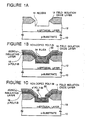
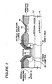
- FIG. 1A to 1G there are diagrammatic sectional views illustrating various steps of an embodiment of the semiconductor device manufacturing method in accordance with the present invention.
- an n-type epitaxial layer 12 is formed, and then, a field isolation oxide layer 14 is formed by a selective oxidation such as a local oxidation of silicon, so that a device formation zone is defined.
- This field isolation oxide layer 14 extends downwardly into the n-type epitaxial layer 12 to a depth deeper than a principal surface of the substrate.
- the device formation zone which is not covered by the field isolation oxide layer 14 is etched by using the field isolation oxide layer 14 as a mask, so that a recess 16 having a depth of 300nm to 500nm is formed in a self-alignment with the field isolation oxide layer 14, as shown in Figure 1A.
- a p-type polycrystalline silicon layer 18 having a thickness of 200nm to 400nm is deposited to cover an inner surface of the recess 16 and an upper surface of the field isolation oxide layer 14, and further etched to form a desired pattern of p-type polycrystalline silicon layer 18 which functions as a base electrode and conductor.
- an insulating layer 20 such as a silicon oxide layer having a thickness of 200nm to 400nm is formed to cover the patterned p-type polycrystalline silicon layer 18, and a polycrystalline silicon layer 22 having a thickness of 200nm is deposited to cover the insulating layer 20.
- This polycrystalline silicon layer 22 is doped with no impurity.
- a silica film formation solution containing 4 to 12 mol % of phosphorus is deposited to have a thickness of 100nm to 200nm.
- the substrate is baked at a temperature of about 600°C, and the dried silica is etched to leave a silica film 24 containing the phosphorus only at a bottom of the recess 16.
- the substrate is heat-treated at a temperature of about 900°C, so that the phosphorus contained in the silica film 24 diffuses into the polycrystalline silicon layer 22, so that the polycrystalline silicon layer 22 on the bottom of the recess 16 is converted into an n+ polycrystalline silicon layer 26.
- the silica film 24 is removed by a hydrofluoric acid (HF), as shown in Figure 1C.
- the non-doped polycrystalline silicon layer 22 and the n+ polycrystalline silicon layer 26 are etched by a reactive ion etching using a gas including carbon and chlorine.
- a reactive ion etching since the etching rate for the n+ polycrystalline silicon layer 26 is about double of that for the non-doped polycrystalline silicon layer 22, the n+ polycrystalline silicon layer 26 on the bottom of the recess 16 are removed in a self-alignment manner, and on the other hand, the non-doped polycrystalline silicon layer 22 remains.
- an exposed insulating layer 20 is anisotropically etched by a reactive ion etching using a fluorocarbon gas, by using the remaining non-doped polycrystalline silicon layer 22 as a mask, as shown in Figure 1D.
- the exposed n-type epitaxial layer 12 within the opening is heat-oxidized to form an silicon oxide layer 30 on the n-type epitaxial layer 12.
- p-type impurities for example, boron
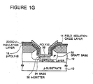
- p-type impurities contained in the p-type polycrystalline silicon layer 18 is diffused into the n-type epitaxial layer 12, so that a p+ graft base region 32 is formed, as shown in Figure 1F.
- p-type impurities is ion-implanted into the bottom of the recess 16 through the oxide layer 30, so that a p-type active base region 34 is formed integrally with the p+ graft base region 32 under the oxide layer 30.
- the oxide layer 30 is anisotropically removed by a reactive ion etching, and thereafter, a polycrystalline silicon layer 36 is deposited on the exposed p-type base region 34. Then, arsenic is ion-implanted to the deposited polycrystalline silicon layer 36 and through deposited polycrystalline silicon layer 36 to the p-type base region 32, so that an n-type emitter region 38 is formed in the p-type base region 32. Thereafter, the arsenic-doped deposited polycrystalline silicon layer 36 is patterned.
- the patterned p-type polycrystalline silicon layer 18 formes base electrode and wiring conductor, and the patterned arsenic-doped deposited polycrystalline silicon layer 36 forms an emitter electrode and wiring conductor.
- a collector electrode and wiring conductor 40 is formed in contact with an n+ region 42 formed in the n-type epitaxial layer 12.
- an npn bipolar transistor is formed.
- the p-type polycrystalline silicon layer 18 functioning as the base electrode and wiring conductor extends from the graft base region 32 along a vertical wall of the recess 16 formed in alignment with the field isolation oxide 14, and also extends from an upper edge fo the recess 16 directly onto the field isolation oxide 14. Namely, there is no thin insulating layer formed at the inside of the field isolation oxide. Therefore, the p-type silicon layer 18 extending from the graft base region has no portion extending over the thin insulating layer formed at the inside of the field isolation oxide. In other words, the p-type silicon layer 18 extending from the graft base region and the n type epitaxial layer 12 forming the collector region are separated only by the thick field isolation oxide.
- a MOS parasitic capacitance between the collector region 12 and the base electrode and wiring conductor 18 can be greatly reduced as compared with the conventional one in which a portion of a base electrode and wiring conductor extends over the insulating layer formed at the inside of the field isolation oxide.
- the diffusion source for formation of the graft base region 32 has a horizontal size (or length or width) corresponding to a sum of the thickness of the p-type silicon layer 18 and the thickness of the insulating layer 20.
- the thickness of the p-type silicon layer 18 and the thickness of the insulating layer 20 are precisely controlled. Therefore, the diffusion source for formation of the graft base region 32 can have a precisely controlled horizontal size, as compared with the diffusion source formed under the overhanging edge portion of the insulating layer in the conventional process, since the amount of overhang is difficult to control.
- the thick oxide layer 14 for a device isolation is selectively formed, and the graft base region 32 is formed in alignment with an edge of the device isolation thick oxide layer 14, and thereafter, the emitter region 38 is formed in alignment with the base region.
- the device isolation pattern is designed to realize the above mentioned relation, a plurality of different diffusion layers are all formed in a self-alignment manner. Therefore, it is not necessary to provide for a margin including an amount of mismatching between different patterns, and accordingly, it is possible to reduce a transistor to a minimum size required.
- the number of mask patterns used can be reduced by three or four as compared with the conventional method.
Landscapes
- Bipolar Transistors (AREA)
Applications Claiming Priority (2)
| Application Number | Priority Date | Filing Date | Title |
|---|---|---|---|
| JP63308210A JPH06101473B2 (ja) | 1988-12-05 | 1988-12-05 | 半導体装置 |
| JP308210/88 | 1988-12-05 |
Publications (3)
| Publication Number | Publication Date |
|---|---|
| EP0372476A2 true EP0372476A2 (fr) | 1990-06-13 |
| EP0372476A3 EP0372476A3 (en) | 1990-08-08 |
| EP0372476B1 EP0372476B1 (fr) | 1994-08-10 |
Family
ID=17978246
Family Applications (1)
| Application Number | Title | Priority Date | Filing Date |
|---|---|---|---|
| EP89122383A Expired - Lifetime EP0372476B1 (fr) | 1988-12-05 | 1989-12-05 | Dispositif semi-conducteur ayant une capacité parasite réduite et méthode pour sa fabrication |
Country Status (4)
| Country | Link |
|---|---|
| US (1) | US4980302A (fr) |
| EP (1) | EP0372476B1 (fr) |
| JP (1) | JPH06101473B2 (fr) |
| DE (1) | DE68917434T2 (fr) |
Cited By (3)
| Publication number | Priority date | Publication date | Assignee | Title |
|---|---|---|---|---|
| EP0589631A1 (fr) * | 1992-09-25 | 1994-03-30 | STMicroelectronics, Inc. | Structure de base encastrée, auto-alignée, avec une résistance basse |
| EP0843351A1 (fr) * | 1996-11-19 | 1998-05-20 | STMicroelectronics S.A. | Procédé de fabrication d'un transistor NPN dans une technologie BICMOS |
| DE19845790A1 (de) * | 1998-09-21 | 2000-03-23 | Inst Halbleiterphysik Gmbh | Verfahren zur naßchemischen Abdünnung von Si-Schichten im aktiven Emittergebiet eines Bipolartransistors |
Families Citing this family (16)
| Publication number | Priority date | Publication date | Assignee | Title |
|---|---|---|---|---|
| US5283202A (en) * | 1986-03-21 | 1994-02-01 | Advanced Power Technology, Inc. | IGBT device with platinum lifetime control having gradient or profile tailored platinum diffusion regions |
| US5262336A (en) * | 1986-03-21 | 1993-11-16 | Advanced Power Technology, Inc. | IGBT process to produce platinum lifetime control |
| US5528058A (en) * | 1986-03-21 | 1996-06-18 | Advanced Power Technology, Inc. | IGBT device with platinum lifetime control and reduced gaw |
| US5137840A (en) * | 1990-10-24 | 1992-08-11 | International Business Machines Corporation | Vertical bipolar transistor with recessed epitaxially grown intrinsic base region |
| US5274267A (en) * | 1992-01-31 | 1993-12-28 | International Business Machines Corporation | Bipolar transistor with low extrinsic base resistance and low noise |
| US5198376A (en) * | 1992-07-07 | 1993-03-30 | International Business Machines Corporation | Method of forming high performance lateral PNP transistor with buried base contact |
| US5322805A (en) * | 1992-10-16 | 1994-06-21 | Ncr Corporation | Method for forming a bipolar emitter using doped SOG |
| US5478760A (en) * | 1995-03-27 | 1995-12-26 | United Microelectronics Corp. | Process for fabricating a vertical bipolar junction transistor |
| US5482873A (en) * | 1995-04-14 | 1996-01-09 | United Microelectronics Corporation | Method for fabricating a bipolar power transistor |
| US5554543A (en) * | 1995-05-24 | 1996-09-10 | United Microelectronics Corporation | Process for fabricating bipolar junction transistor having reduced parasitic capacitance |
| FR2756100B1 (fr) | 1996-11-19 | 1999-02-12 | Sgs Thomson Microelectronics | Transistor bipolaire a emetteur inhomogene dans un circuit integre bicmos |
| FR2756103B1 (fr) * | 1996-11-19 | 1999-05-14 | Sgs Thomson Microelectronics | Fabrication de circuits integres bipolaires/cmos et d'un condensateur |
| GB2338828A (en) * | 1998-06-26 | 1999-12-29 | Mitel Semiconductor Ltd | Integrated circuit with multiple base width bipolar transistors |
| JP4402953B2 (ja) * | 2001-09-18 | 2010-01-20 | パナソニック株式会社 | 半導体装置の製造方法 |
| JP2009021502A (ja) * | 2007-07-13 | 2009-01-29 | Elpida Memory Inc | 半導体装置およびその製造方法 |
| DE102015213294A1 (de) * | 2015-07-15 | 2017-01-19 | Mahle International Gmbh | Thermoelektrischer Wärmetauscher |
Family Cites Families (4)
| Publication number | Priority date | Publication date | Assignee | Title |
|---|---|---|---|---|
| US4492008A (en) * | 1983-08-04 | 1985-01-08 | International Business Machines Corporation | Methods for making high performance lateral bipolar transistors |
| JPS60223165A (ja) * | 1984-04-19 | 1985-11-07 | Toshiba Corp | 半導体装置の製造方法 |
| EP0170250B1 (fr) * | 1984-07-31 | 1990-10-24 | Kabushiki Kaisha Toshiba | Transistor bipolaire et son procédé de fabrication |
| US4847670A (en) * | 1987-05-11 | 1989-07-11 | International Business Machines Corporation | High performance sidewall emitter transistor |
-
1988
- 1988-12-05 JP JP63308210A patent/JPH06101473B2/ja not_active Expired - Lifetime
-
1989
- 1989-12-05 DE DE68917434T patent/DE68917434T2/de not_active Expired - Fee Related
- 1989-12-05 EP EP89122383A patent/EP0372476B1/fr not_active Expired - Lifetime
- 1989-12-05 US US07/446,364 patent/US4980302A/en not_active Expired - Fee Related
Cited By (6)
| Publication number | Priority date | Publication date | Assignee | Title |
|---|---|---|---|---|
| EP0589631A1 (fr) * | 1992-09-25 | 1994-03-30 | STMicroelectronics, Inc. | Structure de base encastrée, auto-alignée, avec une résistance basse |
| US5328857A (en) * | 1992-09-25 | 1994-07-12 | Sgs-Thomson Microelectronics, Inc. | Method of forming a bilevel, self aligned, low base resistance semiconductor structure |
| EP0843351A1 (fr) * | 1996-11-19 | 1998-05-20 | STMicroelectronics S.A. | Procédé de fabrication d'un transistor NPN dans une technologie BICMOS |
| FR2756101A1 (fr) * | 1996-11-19 | 1998-05-22 | Sgs Thomson Microelectronics | Procede de fabrication d'un transistor npn dans une technologie bicmos |
| DE19845790A1 (de) * | 1998-09-21 | 2000-03-23 | Inst Halbleiterphysik Gmbh | Verfahren zur naßchemischen Abdünnung von Si-Schichten im aktiven Emittergebiet eines Bipolartransistors |
| DE19845790B4 (de) * | 1998-09-21 | 2008-12-04 | IHP GmbH - Innovations for High Performance Microelectronics/Institut für innovative Mikroelektronik | Verfahren zur naßchemischen Abdünnung von Si-Schichten im aktiven Emittergebiet eines Bipolartransistors |
Also Published As
| Publication number | Publication date |
|---|---|
| DE68917434T2 (de) | 1995-03-30 |
| EP0372476B1 (fr) | 1994-08-10 |
| JPH02153536A (ja) | 1990-06-13 |
| US4980302A (en) | 1990-12-25 |
| DE68917434D1 (de) | 1994-09-15 |
| JPH06101473B2 (ja) | 1994-12-12 |
| EP0372476A3 (en) | 1990-08-08 |
Similar Documents
| Publication | Publication Date | Title |
|---|---|---|
| US4318751A (en) | Self-aligned process for providing an improved high performance bipolar transistor | |
| EP0372476B1 (fr) | Dispositif semi-conducteur ayant une capacité parasite réduite et méthode pour sa fabrication | |
| EP0061729B1 (fr) | Procédé pour la fabrication de structures comportant des composants semiconducteurs intégrés à configuration mésa et structures de ce type | |
| US4252582A (en) | Self aligned method for making bipolar transistor having minimum base to emitter contact spacing | |
| US4839305A (en) | Method of making single polysilicon self-aligned transistor | |
| US4994400A (en) | Method of fabricating a semiconductor device using a tri-layer structure and conductive sidewalls | |
| KR100207337B1 (ko) | 반도체장치 및 그 제조방법 | |
| EP0083816B1 (fr) | Dispositif semi-conducteur comprenant une configuration d'interconnexion | |
| US4997775A (en) | Method for forming a complementary bipolar transistor structure including a self-aligned vertical PNP transistor | |
| US3933528A (en) | Process for fabricating integrated circuits utilizing ion implantation | |
| EP0051534B1 (fr) | Procédé de fabrication auto-alignée de structures de circuits intégrés employant différents taux de croissance de l'oxyde | |
| JP2700487B2 (ja) | バイポーラ集積回路及びその製造方法 | |
| US4866000A (en) | Fabrication method for semiconductor integrated circuits | |
| JP2501806B2 (ja) | 壁スペ−サを有するバイポ−ラ半導体装置の製造方法 | |
| US4740478A (en) | Integrated circuit method using double implant doping | |
| EP0300514B1 (fr) | Dispositif semi-conducteur ayant une structure de contact latérale et son procédé de fabrication | |
| EP0070499B1 (fr) | Procédé de fabrication d'un dispositif semiconducteur | |
| US5571731A (en) | Procedure for the manufacture of bipolar transistors without epitaxy and with fully implanted base and collector regions which are self-positioning relative to each other | |
| JP3923620B2 (ja) | 半導体基板の製造方法 | |
| US4910575A (en) | Semiconductor integrated circuit and its manufacturing method | |
| EP0260058A1 (fr) | Procédé auto-aligné pour fabriquer des dispositifs semi-conducteurs du type bipolaire | |
| JP2615707B2 (ja) | 半導体装置の製造方法 | |
| EP0367293A2 (fr) | Dispositif semi-conducteur avec base auto-alignée et méthode de sa fabrication | |
| US5328856A (en) | Method for producing bipolar transistors having polysilicon contacted terminals | |
| KR0123686Y1 (ko) | 바이폴라 트랜지스터 |
Legal Events
| Date | Code | Title | Description |
|---|---|---|---|
| PUAI | Public reference made under article 153(3) epc to a published international application that has entered the european phase |
Free format text: ORIGINAL CODE: 0009012 |
|
| 17P | Request for examination filed |
Effective date: 19891205 |
|
| AK | Designated contracting states |
Kind code of ref document: A2 Designated state(s): DE FR GB |
|
| PUAL | Search report despatched |
Free format text: ORIGINAL CODE: 0009013 |
|
| AK | Designated contracting states |
Kind code of ref document: A3 Designated state(s): DE FR GB |
|
| 17Q | First examination report despatched |
Effective date: 19931001 |
|
| GRAA | (expected) grant |
Free format text: ORIGINAL CODE: 0009210 |
|
| AK | Designated contracting states |
Kind code of ref document: B1 Designated state(s): DE FR GB |
|
| REF | Corresponds to: |
Ref document number: 68917434 Country of ref document: DE Date of ref document: 19940915 |
|
| ET | Fr: translation filed | ||
| PLBE | No opposition filed within time limit |
Free format text: ORIGINAL CODE: 0009261 |
|
| STAA | Information on the status of an ep patent application or granted ep patent |
Free format text: STATUS: NO OPPOSITION FILED WITHIN TIME LIMIT |
|
| 26N | No opposition filed | ||
| PGFP | Annual fee paid to national office [announced via postgrant information from national office to epo] |
Ref country code: GB Payment date: 20011205 Year of fee payment: 13 |
|
| PGFP | Annual fee paid to national office [announced via postgrant information from national office to epo] |
Ref country code: FR Payment date: 20011212 Year of fee payment: 13 |
|
| PGFP | Annual fee paid to national office [announced via postgrant information from national office to epo] |
Ref country code: DE Payment date: 20011217 Year of fee payment: 13 |
|
| REG | Reference to a national code |
Ref country code: GB Ref legal event code: IF02 |
|
| PG25 | Lapsed in a contracting state [announced via postgrant information from national office to epo] |
Ref country code: GB Free format text: LAPSE BECAUSE OF NON-PAYMENT OF DUE FEES Effective date: 20021205 |
|
| PG25 | Lapsed in a contracting state [announced via postgrant information from national office to epo] |
Ref country code: DE Free format text: LAPSE BECAUSE OF NON-PAYMENT OF DUE FEES Effective date: 20030701 |
|
| GBPC | Gb: european patent ceased through non-payment of renewal fee | ||
| PG25 | Lapsed in a contracting state [announced via postgrant information from national office to epo] |
Ref country code: FR Free format text: LAPSE BECAUSE OF NON-PAYMENT OF DUE FEES Effective date: 20030901 |
|
| REG | Reference to a national code |
Ref country code: FR Ref legal event code: ST |