EP0589631A1 - Structure de base encastrée, auto-alignée, avec une résistance basse - Google Patents
Structure de base encastrée, auto-alignée, avec une résistance basse Download PDFInfo
- Publication number
- EP0589631A1 EP0589631A1 EP93307352A EP93307352A EP0589631A1 EP 0589631 A1 EP0589631 A1 EP 0589631A1 EP 93307352 A EP93307352 A EP 93307352A EP 93307352 A EP93307352 A EP 93307352A EP 0589631 A1 EP0589631 A1 EP 0589631A1
- Authority
- EP
- European Patent Office
- Prior art keywords
- base
- semiconductor device
- emitter
- surface region
- region
- Prior art date
- Legal status (The legal status is an assumption and is not a legal conclusion. Google has not performed a legal analysis and makes no representation as to the accuracy of the status listed.)
- Granted
Links
Images


Classifications
-
- H—ELECTRICITY
- H10—SEMICONDUCTOR DEVICES; ELECTRIC SOLID-STATE DEVICES NOT OTHERWISE PROVIDED FOR
- H10D—INORGANIC ELECTRIC SEMICONDUCTOR DEVICES
- H10D10/00—Bipolar junction transistors [BJT]
- H10D10/01—Manufacture or treatment
- H10D10/051—Manufacture or treatment of vertical BJTs
- H10D10/056—Manufacture or treatment of vertical BJTs of vertical BJTs having the main current going through the whole substrate, e.g. power BJTs
- H10D10/058—Manufacture or treatment of vertical BJTs of vertical BJTs having the main current going through the whole substrate, e.g. power BJTs having multi-emitter structures, e.g. interdigitated, multi-cellular or distributed emitters
-
- H—ELECTRICITY
- H10—SEMICONDUCTOR DEVICES; ELECTRIC SOLID-STATE DEVICES NOT OTHERWISE PROVIDED FOR
- H10D—INORGANIC ELECTRIC SEMICONDUCTOR DEVICES
- H10D62/00—Semiconductor bodies, or regions thereof, of devices having potential barriers
- H10D62/10—Shapes, relative sizes or dispositions of the regions of the semiconductor bodies; Shapes of the semiconductor bodies
- H10D62/13—Semiconductor regions connected to electrodes carrying current to be rectified, amplified or switched, e.g. source or drain regions
- H10D62/133—Emitter regions of BJTs
-
- H—ELECTRICITY
- H10—SEMICONDUCTOR DEVICES; ELECTRIC SOLID-STATE DEVICES NOT OTHERWISE PROVIDED FOR
- H10D—INORGANIC ELECTRIC SEMICONDUCTOR DEVICES
- H10D62/00—Semiconductor bodies, or regions thereof, of devices having potential barriers
- H10D62/10—Shapes, relative sizes or dispositions of the regions of the semiconductor bodies; Shapes of the semiconductor bodies
- H10D62/17—Semiconductor regions connected to electrodes not carrying current to be rectified, amplified or switched, e.g. channel regions
- H10D62/177—Base regions of bipolar transistors, e.g. BJTs or IGBTs
-
- Y—GENERAL TAGGING OF NEW TECHNOLOGICAL DEVELOPMENTS; GENERAL TAGGING OF CROSS-SECTIONAL TECHNOLOGIES SPANNING OVER SEVERAL SECTIONS OF THE IPC; TECHNICAL SUBJECTS COVERED BY FORMER USPC CROSS-REFERENCE ART COLLECTIONS [XRACs] AND DIGESTS
- Y10—TECHNICAL SUBJECTS COVERED BY FORMER USPC
- Y10S—TECHNICAL SUBJECTS COVERED BY FORMER USPC CROSS-REFERENCE ART COLLECTIONS [XRACs] AND DIGESTS
- Y10S148/00—Metal treatment
- Y10S148/01—Bipolar transistors-ion implantation
-
- Y—GENERAL TAGGING OF NEW TECHNOLOGICAL DEVELOPMENTS; GENERAL TAGGING OF CROSS-SECTIONAL TECHNOLOGIES SPANNING OVER SEVERAL SECTIONS OF THE IPC; TECHNICAL SUBJECTS COVERED BY FORMER USPC CROSS-REFERENCE ART COLLECTIONS [XRACs] AND DIGESTS
- Y10—TECHNICAL SUBJECTS COVERED BY FORMER USPC
- Y10S—TECHNICAL SUBJECTS COVERED BY FORMER USPC CROSS-REFERENCE ART COLLECTIONS [XRACs] AND DIGESTS
- Y10S148/00—Metal treatment
- Y10S148/102—Mask alignment
Definitions
- the present invention relates to semiconductor devices, and more particularly, to a method of manufacturing a semiconductor device having automatically aligned structures.
- figures of merit may be used to describe the performance of a semiconductor device.
- One figure of merit of particular interest is defined as the numerical ratio between the emitter periphery (EP) and the base area (BA).
- EP emitter periphery
- BA base area
- a device demonstrates improved current handling capability.
- a device is able to handle high power with low parasitic capacitance.
- such a device is highly suitable for high frequency applications (for example, at radio frequencies).
- One way of increasing a device's figure of merit is by decreasing the "pitch" or spacing between repetitive patterns, i.e.-emitters. Due to the fact that integrated circuits typically have a planar structure, current that flows from the emitter to the collector typically travels parallel to the surface of the wafer after being transported vertically through the base. This current then flows upward towards a contact located on the wafer surface. Due to the significant resistivity of current-flow paths within the device, parasitic series resistances exist.
- R BB intrinsic base region
- the base area of a device may be readily decreased using appropriate photolithographic processes. However, current photolithographic processes are unable to produce device features smaller than 1 micron.
- a base area which is-too small may lead to poor device performance.
- the spacings from base contact to emitter edge are large enough to allow a small amount of depletion so that proper device operation is obtained.
- the spacing in selected portions of the device reaches zero, a short may occur, causing the device to become completely inoperative.
- a semiconductor device is manufactured by placing an insulating layer over a portion of a surface region and introducing a dopant to a further portion of the surface region. Selected areas of the further portion of the surface region are covered with insulating layer portions while the uncovered portions of the surface region are isotropically etched to create a plurality of recesses. The insulating layer portions partially overhang the created recesses. A dopant is added to form a base. A further dopant is then added between the overhanging portions of the insulating layer to form a plurality of emitter zones.
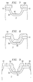
- Figures 1-5, 6A and 7-9 are cross sectional views illustrating a process for forming a bilevel, self aligned, low base resistance structure in accordance with the present invention.
- Figure 6B is a top view of a semiconductor device at the stage of manufacture illustrated by Figure 6A.
- Figure 6B additionally indicates exemplary contact connections.
- Figure 6A is a cross sectional view of Figure 6B taken in the plane X-X'.
- Figures 1-9 An exemplary embodiment of the present invention will now be described more fully with reference to Figures 1-9, in which a semiconductor device is shown during successive stages of manufacture.
- Figures 1-6 show a side view of a relatively large portion of the semiconductor device.
- Figure 6B shows a top view of the semiconductor device.
- Figures 7-9 show a relatively close side view of the device, and in particular, provide a detailed view of a portion of the semiconductor device which includes a single emitter.
- a semiconductor device can be manufactured in accordance with an exemplary embodiment of the present invention, in the following manner.
- the starting material is a semiconductor wafer, in this example of n-type silicon, including n-type epitaxial silicon layer 2 having a thickness of about 5 microns and a resistivity of about 1 ohm cm, which is grown on a substrate 1 of highly doped n-type silicon having a resistivity of, for example, .002 ohm cm.
- the epitaxial growth method is known in the art, and is not described. Other thicknesses and/or dopings are possible and will be chosen by those skilled in the art in accordance with existing conditions.
- oxide layer 3 is formed on epitaxial layer 2.
- Oxide layer 3 in this embodiment is a silicon oxide layer having a thickness of, for example, 1/2 micron and which is formed, for example, by thermal oxidation. Openings 5 are then formed in oxide layer 3 by photolithographic etching.
- Oxide layer 3 selectively masks against this implantation.
- breakdown enhancement regions 9 are optionally formed inside silicon layer 2 and substrate 1 using well known diffusion techniques.
- the wafer is placed in a diffusion furnace so as to diffuse the low conductivity P- diffusion region into the wafer.
- This diffusion step is preferably performed in a nitrogen and an oxygen environment.
- an oxide coating 6 is formed in previously exposed openings 5.
- a photoresist 20 is formed over selected portions of oxide layer 3.
- the wafer is then subjected to an etching ambient, causing the exposed portions of oxide layer 3 to be removed.
- the wafer is then subjected to a P+ implant, such as B11 - 5 x 10¹⁵ - 25 KeV, to form P+ region 10.
- photoresist 20 is removed and another oxide layer 25 is deposited via low temperature (350 - 400 C) glass deposition.
- Oxide layer 25 is preferably formed with a thickness ranging from 1500 to 2500 angstroms.
- selected portions of oxide layer 25 are then removed, thus exposing the sites at which the emitters will be formed.
- selected portions of oxide layer 25 portions 25 a-z
- oxide portions 25 a-z being used as a plurality of masks, the wafer is subjected to isotropic etching. This is shown in Figure 6A.
- surface preparation for the etch is particularly desirable to the generation of a smooth silicon surface for the base and emitter implants. If the surface is damaged, poor radio frequency device performance as well as direct current parameter degradation may result. Furthermore, because it has been determined that the surface prior to etch is desirably exceptionally clean and free of oxide, oxide removal may be accomplished immediately prior to the dry etch step.
- oxide portions 25 a-z each extend above portions of exposed substrate 1.
- oxide portions 25 a-z form a plurality of "overhanging shelves".
- These shelves define a plurality of windows through which ion implantation may occur.
- this etchant is a gas mixture comprising tetrafluoromethane (CF4) halocarbon 13B1 and oxygen (O2) in ratios of approximately 90:5:5 % (by weight).
- this etch is accomplished with a Tegal 700 etcher.
- a two part vertical for one part lateral etch ratio is obtained. It is extremely desirable to obtain this type of "sloped" edge to maintain good step coverage for later metalization.
- a base implant is provided to ensure that there is a continuous current path to the remaining portion of silicon layer 2.
- This continuous current path is extremely desirable because the current flow between the emitter and the base depends on the continuity of the base between the emitter and the P+ implant.
- the base implantation energy is desirably chosen to allow at least partial penetration of the overhanging shelves formed by oxide portions 25 a-z.
- the wafer is treated with a P type doping impurity to diffuse a P-type region 30 into the base site.
- a P type doping impurity to diffuse a P-type region 30 into the base site.
- Figure 6B A top view of the semiconductor device at the stage of manufacture corresponding to Figure 6A is illustrated by Figure 6B.
- Figure 6B additionally indicates exemplary contact connections.
- Figure 6A is a cross sectional view of Figure 6B taken in the plane X-X'.
- Corresponding letters in Figures 6A and 6B are used to refer to corresponding structures.
- n-type (arsenic) ions are implanted to form emitter region 40.
- the portion of the wafer shown in Figure 7 is an enlarged view of the wafer shown in Figure 6.
- the overhanging shelves of oxide layers 25a-z shown in Figure 7 ensure precise positioning (self-alignment) of the emitter peripheries in P+ region 30.
- oxide layer 50 is deposited. This is shown in Figure 8. Selected portions of oxide layer 50 are then removed (using, for example, photolithography) as shown in Figure 9. In this manner, device isolation is achieved. The base, emitter and P+ regions are then driven simultaneously. In another exemplary embodiment of the present invention, the base and P+ regions are partially driven prior to implantation of the emitter region. In a still further exemplary embodiment of the present invention, oxide portions 25 a-z are not removed and oxide layer 50 is deposited directly on oxide portions 25 a-z. This is because, for example, discontinuities may result in metalization layers applied above oxide portions 25a-z. In some devices, however, (for example, overlay devices) the non-removal of oxide portions 25 a-z does not substantially effect device performance.
- the various structures within this device can be carefully aligned.
- the intrinsic base region can be formed with a length of approximately 1000 angstroms, thus resulting in a 40% increase in the maximum frequency capabilities over prior art devices.
- the figure of merit of a device formed using the above described method can be as high as 15. This results in an additional 40% increase in maximum frequency capabilities over prior art devices.
- These increases in frequency capabilities may result in a doubling of gain in the device. This results in a half-octave-improvement in frequency capability (i.e. increasing maximum frequency of operation from 4 GHZ to 6 GHZ for silicon technology).
- processing steps of the present invention are significantly simplified over that of many prior art devices, thus reducing the number of photoresist, process and high temperature steps.
Landscapes
- Bipolar Transistors (AREA)
Applications Claiming Priority (2)
| Application Number | Priority Date | Filing Date | Title |
|---|---|---|---|
| US951162 | 1992-09-25 | ||
| US07/951,162 US5328857A (en) | 1992-09-25 | 1992-09-25 | Method of forming a bilevel, self aligned, low base resistance semiconductor structure |
Publications (2)
| Publication Number | Publication Date |
|---|---|
| EP0589631A1 true EP0589631A1 (fr) | 1994-03-30 |
| EP0589631B1 EP0589631B1 (fr) | 1998-12-02 |
Family
ID=25491349
Family Applications (1)
| Application Number | Title | Priority Date | Filing Date |
|---|---|---|---|
| EP93307352A Expired - Lifetime EP0589631B1 (fr) | 1992-09-25 | 1993-09-17 | Procédé de fabrication d'une structure de base encastrée, auto-alignée, avec une résistance basse |
Country Status (3)
| Country | Link |
|---|---|
| US (1) | US5328857A (fr) |
| EP (1) | EP0589631B1 (fr) |
| DE (1) | DE69322348T2 (fr) |
Cited By (2)
| Publication number | Priority date | Publication date | Assignee | Title |
|---|---|---|---|---|
| WO1999007011A1 (fr) * | 1997-07-31 | 1999-02-11 | Siemens Aktiengesellschaft | Procede de structuration de semi-conducteurs, avec une haute precision, une bonne homogeneite et une bonne reproductibilite |
| GB2385463A (en) * | 2001-10-22 | 2003-08-20 | Asb Inc | Bipolar transistor |
Families Citing this family (3)
| Publication number | Priority date | Publication date | Assignee | Title |
|---|---|---|---|---|
| US5416032A (en) * | 1994-06-24 | 1995-05-16 | Sgs-Thomson Microelectronics, Inc. | Method of making a high conductivity p-plus region for self-aligned, shallow diffused, bipolar transistors |
| US5455449A (en) * | 1994-06-30 | 1995-10-03 | National Semiconductor Corporation | Offset lattice bipolar transistor architecture |
| US5631495A (en) * | 1994-11-29 | 1997-05-20 | International Business Machines Corporation | High performance bipolar devices with plurality of base contact regions formed around the emitter layer |
Citations (2)
| Publication number | Priority date | Publication date | Assignee | Title |
|---|---|---|---|---|
| EP0372476A2 (fr) * | 1988-12-05 | 1990-06-13 | Nec Corporation | Dispositif semi-conducteur ayant une capacité parasite réduite et méthode pour sa fabrication |
| EP0438693A2 (fr) * | 1990-01-26 | 1991-07-31 | Kabushiki Kaisha Toshiba | Procédé de fabrication d'un dispositif semi-conducteur |
Family Cites Families (6)
| Publication number | Priority date | Publication date | Assignee | Title |
|---|---|---|---|---|
| US4433470A (en) * | 1981-05-19 | 1984-02-28 | Tokyo Shibaura Denki Kabushiki Kaisha | Method for manufacturing semiconductor device utilizing selective etching and diffusion |
| US4539742A (en) * | 1981-06-22 | 1985-09-10 | Tokyo Shibaura Denki Kabushiki Kaisha | Semiconductor device and method for manufacturing the same |
| US4433471A (en) * | 1982-01-18 | 1984-02-28 | Fairchild Camera & Instrument Corporation | Method for the formation of high density memory cells using ion implantation techniques |
| US4625388A (en) * | 1982-04-26 | 1986-12-02 | Acrian, Inc. | Method of fabricating mesa MOSFET using overhang mask and resulting structure |
| US4510016A (en) * | 1982-12-09 | 1985-04-09 | Gte Laboratories | Method of fabricating submicron silicon structures such as permeable base transistors |
| JPS63249370A (ja) * | 1987-04-06 | 1988-10-17 | Toshiba Corp | 半導体装置およびその製造方法 |
-
1992
- 1992-09-25 US US07/951,162 patent/US5328857A/en not_active Expired - Lifetime
-
1993
- 1993-09-17 DE DE69322348T patent/DE69322348T2/de not_active Expired - Fee Related
- 1993-09-17 EP EP93307352A patent/EP0589631B1/fr not_active Expired - Lifetime
Patent Citations (2)
| Publication number | Priority date | Publication date | Assignee | Title |
|---|---|---|---|---|
| EP0372476A2 (fr) * | 1988-12-05 | 1990-06-13 | Nec Corporation | Dispositif semi-conducteur ayant une capacité parasite réduite et méthode pour sa fabrication |
| EP0438693A2 (fr) * | 1990-01-26 | 1991-07-31 | Kabushiki Kaisha Toshiba | Procédé de fabrication d'un dispositif semi-conducteur |
Non-Patent Citations (1)
| Title |
|---|
| 1992 SYMPOSIUM ON VLSI TECHNOLOGY 2 June 1992, SEATLLE pages 54 - 55 T. ONAI ET AL. * |
Cited By (3)
| Publication number | Priority date | Publication date | Assignee | Title |
|---|---|---|---|---|
| WO1999007011A1 (fr) * | 1997-07-31 | 1999-02-11 | Siemens Aktiengesellschaft | Procede de structuration de semi-conducteurs, avec une haute precision, une bonne homogeneite et une bonne reproductibilite |
| US6204135B1 (en) | 1997-07-31 | 2001-03-20 | Siced Electronics Development Gmbh & Co Kg | Method for patterning semiconductors with high precision, good homogeneity and reproducibility |
| GB2385463A (en) * | 2001-10-22 | 2003-08-20 | Asb Inc | Bipolar transistor |
Also Published As
| Publication number | Publication date |
|---|---|
| DE69322348T2 (de) | 1999-04-29 |
| EP0589631B1 (fr) | 1998-12-02 |
| DE69322348D1 (de) | 1999-01-14 |
| US5328857A (en) | 1994-07-12 |
Similar Documents
| Publication | Publication Date | Title |
|---|---|---|
| KR100349729B1 (ko) | 바이폴라트랜지스터의베이스형성시의경사주입사용법 | |
| US4619036A (en) | Self-aligned low-temperature emitter drive-in | |
| EP0052198A2 (fr) | Procédé de fabrication de dispositifs semiconducteurs utilisant des techniques d'autoalignement | |
| KR970011641B1 (ko) | 반도체 장치 및 제조방법 | |
| EP0051534A2 (fr) | Procédé de fabrication auto-alignée de structures de circuits intégrés employant différents taux de croissance de l'oxyde | |
| KR0128339B1 (ko) | Cmos 기술을 이용하는 바이폴라 트랜지스터 제조방법 | |
| US5804476A (en) | Method of forming BiCMOS devices having mosfet and bipolar sections therein | |
| EP0137992A2 (fr) | Transistor bipolaire latéral réalisé dans un substrat isolant recouvert de silicium (SOI) | |
| US5328857A (en) | Method of forming a bilevel, self aligned, low base resistance semiconductor structure | |
| KR0154304B1 (ko) | Bicmos장치의 제조방법 | |
| US4721685A (en) | Single layer poly fabrication method and device with shallow emitter/base junctions and optimized channel stopper | |
| EP0036499B1 (fr) | Procédé auto-aligné pour transistor bipolaire à base en polysilicium | |
| KR100245813B1 (ko) | 자기정합형 더블 폴리실리콘 바이폴라 트랜지스터및 그의 제조방법 | |
| US6774455B2 (en) | Semiconductor device with a collector contact in a depressed well-region | |
| JPS62113471A (ja) | バイポ−ラトランジスタに浅く、大量にド−プされた外因性ベ−ス領域を形成する方法 | |
| US5747374A (en) | Methods of fabricating bipolar transistors having separately formed intrinsic base and link-up regions | |
| US6740562B2 (en) | Manufacturing method of a semiconductor device having a polysilicon electrode | |
| US6806159B2 (en) | Method for manufacturing a semiconductor device with sinker contact region | |
| US5376563A (en) | Method of manufacturing an emitter base self alignment structure | |
| KR100210330B1 (ko) | 바이폴라 소자 및 이의 제조 방법 | |
| US7164186B2 (en) | Structure of semiconductor device with sinker contact region | |
| US5013672A (en) | Manufacturing process for high-frequency bipolar transistors | |
| EP0619612B1 (fr) | Méthode de fabrication d'un dispositif semi-conducteur comprenant un transistor bipolaire | |
| KR950000137B1 (ko) | 반도체 장치의 제조방법 | |
| KR940007452B1 (ko) | 반도체 장치의 제조방법 |
Legal Events
| Date | Code | Title | Description |
|---|---|---|---|
| PUAI | Public reference made under article 153(3) epc to a published international application that has entered the european phase |
Free format text: ORIGINAL CODE: 0009012 |
|
| AK | Designated contracting states |
Kind code of ref document: A1 Designated state(s): DE FR GB IT |
|
| 17P | Request for examination filed |
Effective date: 19940901 |
|
| 17Q | First examination report despatched |
Effective date: 19940930 |
|
| GRAG | Despatch of communication of intention to grant |
Free format text: ORIGINAL CODE: EPIDOS AGRA |
|
| GRAG | Despatch of communication of intention to grant |
Free format text: ORIGINAL CODE: EPIDOS AGRA |
|
| GRAH | Despatch of communication of intention to grant a patent |
Free format text: ORIGINAL CODE: EPIDOS IGRA |
|
| GRAH | Despatch of communication of intention to grant a patent |
Free format text: ORIGINAL CODE: EPIDOS IGRA |
|
| GRAA | (expected) grant |
Free format text: ORIGINAL CODE: 0009210 |
|
| RAP1 | Party data changed (applicant data changed or rights of an application transferred) |
Owner name: STMICROELECTRONICS, INC. |
|
| AK | Designated contracting states |
Kind code of ref document: B1 Designated state(s): DE FR GB IT |
|
| REF | Corresponds to: |
Ref document number: 69322348 Country of ref document: DE Date of ref document: 19990114 |
|
| ITF | It: translation for a ep patent filed | ||
| ET | Fr: translation filed | ||
| PG25 | Lapsed in a contracting state [announced via postgrant information from national office to epo] |
Ref country code: GB Free format text: LAPSE BECAUSE OF NON-PAYMENT OF DUE FEES Effective date: 19990917 |
|
| PLBE | No opposition filed within time limit |
Free format text: ORIGINAL CODE: 0009261 |
|
| STAA | Information on the status of an ep patent application or granted ep patent |
Free format text: STATUS: NO OPPOSITION FILED WITHIN TIME LIMIT |
|
| 26N | No opposition filed | ||
| GBPC | Gb: european patent ceased through non-payment of renewal fee |
Effective date: 19990917 |
|
| PG25 | Lapsed in a contracting state [announced via postgrant information from national office to epo] |
Ref country code: FR Free format text: LAPSE BECAUSE OF NON-PAYMENT OF DUE FEES Effective date: 20000531 |
|
| PG25 | Lapsed in a contracting state [announced via postgrant information from national office to epo] |
Ref country code: DE Free format text: LAPSE BECAUSE OF NON-PAYMENT OF DUE FEES Effective date: 20000701 |
|
| REG | Reference to a national code |
Ref country code: FR Ref legal event code: ST |
|
| PG25 | Lapsed in a contracting state [announced via postgrant information from national office to epo] |
Ref country code: IT Free format text: LAPSE BECAUSE OF NON-PAYMENT OF DUE FEES;WARNING: LAPSES OF ITALIAN PATENTS WITH EFFECTIVE DATE BEFORE 2007 MAY HAVE OCCURRED AT ANY TIME BEFORE 2007. THE CORRECT EFFECTIVE DATE MAY BE DIFFERENT FROM THE ONE RECORDED. Effective date: 20050917 |