EP0373832A2 - Dispositif semi-conducteur et appareil de conversion photo-électrique l'utilisant - Google Patents
Dispositif semi-conducteur et appareil de conversion photo-électrique l'utilisant Download PDFInfo
- Publication number
- EP0373832A2 EP0373832A2 EP89312814A EP89312814A EP0373832A2 EP 0373832 A2 EP0373832 A2 EP 0373832A2 EP 89312814 A EP89312814 A EP 89312814A EP 89312814 A EP89312814 A EP 89312814A EP 0373832 A2 EP0373832 A2 EP 0373832A2
- Authority
- EP
- European Patent Office
- Prior art keywords
- emitter
- region
- base
- semiconductor device
- concentration
- Prior art date
- Legal status (The legal status is an assumption and is not a legal conclusion. Google has not performed a legal analysis and makes no representation as to the accuracy of the status listed.)
- Withdrawn
Links
Images




















Classifications
-
- H—ELECTRICITY
- H10—SEMICONDUCTOR DEVICES; ELECTRIC SOLID-STATE DEVICES NOT OTHERWISE PROVIDED FOR
- H10F—INORGANIC SEMICONDUCTOR DEVICES SENSITIVE TO INFRARED RADIATION, LIGHT, ELECTROMAGNETIC RADIATION OF SHORTER WAVELENGTH OR CORPUSCULAR RADIATION
- H10F39/00—Integrated devices, or assemblies of multiple devices, comprising at least one element covered by group H10F30/00, e.g. radiation detectors comprising photodiode arrays
- H10F39/10—Integrated devices
- H10F39/12—Image sensors
- H10F39/197—Bipolar transistor image sensors
-
- H—ELECTRICITY
- H10—SEMICONDUCTOR DEVICES; ELECTRIC SOLID-STATE DEVICES NOT OTHERWISE PROVIDED FOR
- H10F—INORGANIC SEMICONDUCTOR DEVICES SENSITIVE TO INFRARED RADIATION, LIGHT, ELECTROMAGNETIC RADIATION OF SHORTER WAVELENGTH OR CORPUSCULAR RADIATION
- H10F30/00—Individual radiation-sensitive semiconductor devices in which radiation controls the flow of current through the devices, e.g. photodetectors
- H10F30/20—Individual radiation-sensitive semiconductor devices in which radiation controls the flow of current through the devices, e.g. photodetectors the devices having potential barriers, e.g. phototransistors
- H10F30/21—Individual radiation-sensitive semiconductor devices in which radiation controls the flow of current through the devices, e.g. photodetectors the devices having potential barriers, e.g. phototransistors the devices being sensitive to infrared, visible or ultraviolet radiation
- H10F30/24—Individual radiation-sensitive semiconductor devices in which radiation controls the flow of current through the devices, e.g. photodetectors the devices having potential barriers, e.g. phototransistors the devices being sensitive to infrared, visible or ultraviolet radiation the devices having only two potential barriers, e.g. bipolar phototransistors
- H10F30/245—Bipolar phototransistors
Definitions
- the present invention relates to a semiconductor device and a photoelectric conversion apparatus using the device.
- BPT bipolar transistor
- a DOPOSBPT Doped Poly Silicon BPT
- a BPT having a polysilicon emitter is known as a BPT having a shallow junction and a high packing density.
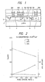
- Fig. 1 is a sectional view showing an example of a conventional BPT.
- reference numeral 1 denotes a substrate made of silicon (Si); 2, an n+-type buried region including material impurity making conductivity into n-type n within Si; 3, an n ⁇ -type region having a low impurity concentration; 4, a p-type region including material (impurity) making conductivity into p-type serving as a base region; 5, an n+-type region including n-type impurity serving as an emitter region; 6, an n-type region serving as a channel stopper; 7, an n+-type region of high impurity concentration for reducing a collector resistance of a bipolar transistor; 101, 102, 103, and 104, insulating films for insulating the element, electrodes, and wirings; 200, an electrode made of a metal, silicide, polycide, or the like.
- the substrate 1 has an n conductivity type upon doping of an impurity such as phosphorus (Ph), antimony (Sb), or arsenic (As), or a p conductivity type upon doping of an impurity such as boron (B), aluminum (Al), or gallium (Ga).
- the buried region 2 need not be necessarily formed. Boron (B), gallium (Ga), or aluminum (Al), and germanium (Ge) are doped in the base region 4.
- the emitter region 5 consists of polysilicon formed by low-pressure chemical vapor deposition (LPCVD).
- the base region 5 consists of a mixed crystal of silicon (Si) and germanium (Ge). Both of Si and Ge are diamond type crystals and perfect solid solutions. Therefore, Si 1-X Ge X is a perfect diamond type crystal for every X (0 to 1). A forbidden band width E g is about 1.1 eV for Si and about 0.7 eV for Ge.
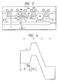
- Fig. 2 is a graph showing a relationship between a mixed crystal ratio X and the forbidden band width E g of Si 1-X Ge X .
- the abscissa represents the mixed crystal ratio X
- the ordinate represents the forbidden band width E g
- a reduction width ⁇ E C at a conduction band side
- a reduction width ⁇ E V at a valence band side As is apparent from Fig. 13, in Si 1-X Ge X , most of a band gap reduction occurs in a valence band. This is very convenient for the hetero BPT because injection of electrons from an emitter to a base is not prevented.
- the BPT of this type comprises a polysilicon emitter region.
- a silicon oxide having a thickness of 10 to 20 ⁇ is formed between the polysilicon emitter region and an emitter region formed by diffusing an impurity from polysilicon to single-crystal silicon.
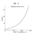
- Fig. 3 is a schematic sectional view showing a conventional BPT.
- reference numeral 1 denotes a substrate; 2, an n+-type buried region; 3, an n ⁇ -type region having a low impurity concentration; 4, a p-type region serving as a base region; 5, an n+-type region serving as an emitter region; 6, an n-type region serving as a channel stopper; 7, an n+-type region for reducing a collector resistance of the bipolar transistor; 8, an oxide film (SiO2) formed between the polysilicon emitter region and the single-crystal emitter region 5; 101, 102, 103, and 104, insulating films for isolating the element, electrodes, and wirings; and 200, electrodes made of a metal, a silicide, a polycide, or the like.
- the substrate 1 has an n conductivity type upon doping of an impurity such as phosphorus (Ph), antimony (Sb), or arsenic (As), or a p conductivity type upon doping of an impurity such as boron (B), aluminum (Al), or gallium (Ga).
- the buried region 2 need not be necessarily formed.
- the n ⁇ -type region 3 is formed by epitaxial techniques. Boron (B), gallium (Ga), or aluminum (Al), and germanium (Ge) are doped in the base region 4.
- the emitter region 5 consists of polysilicon formed by low-pressure chemical vapor deposition (LPCVD).
- This BPT i.e., the BPT having the polysilicon emitter region and the silicon oxide formed between the polysilicon emitter region and the base region, has an advantage in that the oxide film can increase a current gain of the BPT.
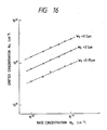
- Fig. 4 shows a diagram showing potentials in the direction of depth of the cross section along the line A-A′ in Fig. 3 in a normal operation.
- reference numeral W E denotes a thickness of an emitter neutral region
- W B a thickness of a base neutral-region.
- a potential barrier is present at a position of W E ′.
- the base current consists of the following two components.
- J B1 (q ⁇ n i 2 ⁇ D P /N E ⁇ L P ) x tanh(W E ′/L P )[exp(V BE /kT)-1]
- Fig. 5 is a schematic sectional view showing a different type of BPT.
- reference numeral 1 denotes a substrate; 2, an n+-type buried region; 3, an n ⁇ -type region having a low impurity concentration; 4, a p-type region serving as a base region; 5, an n+-type region serving as an emitter region; 6, an n-type region serving as a channel stopper; 7, an n+-type region for reducing a collector resistance of the bipolar transistor; 101, 102, 103, and 104, insulating films for insulating the element, electrodes, and wirings; and 200, electrodes made of a metal, a silicide, a polycide, or the like.
- the substrate 1 has an n conductivity type upon doping of an impurity such as phosphorus (Ph), antimony (Sb), or arsenic (As), or a p conductivity type upon doping of an impurity such as boron (B), aluminum (Al), or gallium (Ga).
- the buried region 2 need not be necessarily formed.
- the n ⁇ -type region 3 is formed by epitaxial techniques. Boron (B), gallium (Ga), or aluminum (Al), and germanium (Ge) are doped in the base region 4.
- the emitter region 5 consists of polysilicon.
- the base current consists of the following two components.
- q is a charge
- n i is an intrinsic semiconductor charge density (Si)
- N E is an emitter impurity density
- N B is a base impurity density
- D P is a positive hole diffusion coefficient
- D N is an electron diffusion coefficient
- L P is a positive hole diffusion length ( ⁇ (D P ⁇ P ) 1/2 )
- L N is an electron diffusion length ( D N ⁇ N ) 1/2 )
- k is a Boltzmann constant
- T is an absolute temperature
- V BE represents base-emitter forward biased electrons
- W B is a thickness of the base
- W E is a thickness of the emitter. Note that ⁇ P and ⁇ N are minority carrier lifetimes of the positive
- h FE An influence of the point defect or dislocation on h FE is significantly increased at a low current side of a collector current, and h FE is reduced close to one or below one in some cases.
- the point defect or dislocation at the interface between the Si crystal or Si 1-X Ge X mixed crystal is caused by a difference in lattice coefficients between Si and Si 1-X Ge X .
- FIG. 6 is a graph showing this relationship. Note that this data is obtained when Si 1-X Ge X is deposited on an Si substrate by the MBE method. Since growth is performed at 510°C, a transition region from Si 1-X Ge X to Si is very thin.
- dislocation occurs in the interface if the thickness is not less than that of a hatched region shown in Fig. 6.
- an impurity concentration of the emitter region 5 in the conventional BPT and the conventional DOPOSBPT falls within the range of 1019 to 1021 cm ⁇ 3; an impurity concentration of the base region, 1016 to 1018 cm ⁇ 3; an impurity concentration of the collector region; about 1014 to 1016 cm ⁇ 3.
- a free carrier density is increased (i.e., minority carrier mobility is gradually decreased, and the band gap (forbidden gap width) is decreased).
- the impurity density is 1017 to 1018 or more, band tailing occurs from the ends of the conduction and valence bands in an n- or p-type semiconductor.
- Figs. 7 and 8 are views showing band structures is semiconductors. Energy is plotted along the ordinate and a state density n(E) (i.e., the number of carriers per unit volume) is plotted along the abscissa in each of Figs. 7 and 8.
- Fig. 7 is a view showing a band structure of an n-type semiconductor having a low impurity density. In this case, an n-type donor level is separated from a conduction band.
- Fig. 8 shows a semiconductor containing a high impurity density, and the width of a donor level is increased. The donor level becomes a donor band whose energy is coupled to that of the conduction band unique to the semiconductor. That is, as shown in Fig.
- Band narrowing of the n-type semiconductor has been described in Fig. 8. Similar band tailing occurs on the side of the valence band in a p-type semiconductor having a high impurity concentration, and narrowing of a band width (prohibition band) E g occurs.
- Fig. 9 is a graph showing results of band-gap narrowing width calculations by using equation (5) when boron (B) is doped in Si in a high concentration.
- the impurity density (cm ⁇ 3) of the impurity is plotted along the abscissa in Fig. 9, and the narrowed width ⁇ E g (meV) of the band gap is plotted along the ordinate in Fig. 9.
- the current gain can be expressed when only band-gap narrowing is taken into consideration: h FE ⁇ h FE0 ⁇ exp ⁇ ( ⁇ E gb - ⁇ E ge )/KT ⁇ (8) where h FE0 is a current gain without band-gap narrowing.
- the conventional BPT had an emitter impurity concentration of about 1020 to 1021 cm ⁇ 3, and a base impurity concentration of about 1016 to 1018 cm ⁇ 3. For this reason, ⁇ E ge is large, and ⁇ E gb is almost zero. Therefore, the current gain h FE is smaller than the designed value.
- the impurity concentration of the base When the current gain h FE is to be increased in a shallowed BPT, the impurity concentration of the base must be increased. When the impurity concentration of the base is, however, increased, the base-emitter breakdown voltage is decreased. In addition, the base-emitter capacitance is undesirably increased.
- a frequency f T is only about 1 GHz.
- the photoelectric transducer apparatus of this type is incompatible with HD (high Division; an area sensor coping with high vision).
- a silicon oxide film having a thickness of 10 - 20 ⁇ has been formed between emitter region and base region.
- Such BPT can prevent hall from introducing from base region into emitter region due to a potential barrier formed within a valence band by an oxide film at an interface between the base and emitter. Therefore, the advantage that the current gain can be increased is obtained.
- Fig. 10 shows a potential during a normal operation at A-A′ sectional area wherein a silicon oxide is formed between the emitter and collector regions of semiconductor device in Fig. 6.
- W E denotes a thickness of the emitter nutral area
- W B denotes a thickness of the base nutral area.
- a potential barrier is formed at a position of W E .
- the characteristic variations of the individual BPTs are very important when they occur in a linear IC, a line sensor, and the like.
- the present invention recides in providing a solutions of the above described problems. That is, the present invention provides a semiconductor device not producing a point defect or dislocation in the hetero interface.
- the present invention provides a semiconductor device which has a high current gain h FE , can prevent a decrease in base-emitter breakdown voltage, and has a small capacitance, and a photoelectric transducer apparatus using this semiconductor device.
- the present invention provides a semiconductor device which can minimize characteristic variations and has a high current gain h FE and a high frequency, and a photoelectric transducer apparatus using the same.
- the object of the present invention is to provide a semiconductor device characterized by comprising at least an emitter region of a first conductivity type, a base region of a second conductivity type, and a collector region of a first conductivity type, the base region essentially consisting of Si 1-X Ge X (0 ⁇ X ⁇ 1), further comprising regions formed in a depletion layer close to an interface between the base region and the collector region or in the collector region and in a depletion layer close to an interface between the base region and the emitter region or in the emitter region, and having a larger Ge amount at the base region side and a smaller Ge amount at the emitter and collector sides.
- the another object of the present invention is to achieve in above semiconductor device, that Si 1-X Ge X is 0.0625 ⁇ X ⁇ 0.375.
- the further object of the present invention is to provide a semiconductor device, characterized in that addition of Ge is performed by ion implantation.
- the still further object of the present invention is to provide a photoelectric transducer apparatus characterized by using a semiconductor device.
- the next object of the present invention is to provide a semiconductor device at least having an emitter region of a first conductivity type, a base region of a second conductivity type, and a collector region of a first conductivity type, characterized in that
- the further object of the present invention is to provide a semiconductor device, characterized in that B and Ge are doped in the base region by ion implantation.
- the still further object of the present invention is to provide a semiconductor device, characterized in that N D falls within a range of 1017 to 1019 cm ⁇ 3.
- the still further object of the present invention is to provide a semiconductor device, characterized in that an Si layer having an impurity concentration of 1019 to 1021 cm ⁇ 3 is formed between the emitter region and an electrode.
- the still further object of the present invention is to provide a semiconductor device, characterized in that condition N D ⁇ N B is established.
- the still further object of the present invention is to provide a photoelectric transducer apparatus using the semiconductor device of the first to fifth gists.
- An object of the present invention is to provide a semiconductor device is characterized by a bipolar transistor structure in which an emitter region is deposited on a base region, wherein the emitter region is formed after an oxide on the base region is removed, and the emitter region essentially consists of a single crystal.
- An object of the present invention is to provide a semiconductor device of the present invention, which has at least an emitter of a first conductivity type, a base of a second conductivity type, and a collector of the first conductivity type, is characterized in that at least said base essentially consists of an Si 1-X Ge X crystal (0 ⁇ X ⁇ 1), an interface between the Si 1-X Ge X crystal and an Si crystal is an inclined hetero interface, and a depth of Si 1-X Ge X is the same as or larger than a depth of said base.
- a Ge composition X is smaller in a shallow portion and larger in a deeper portion.
- doping of Ge is performed by ion implantation.
- a photoelectric transducer apparatus of the present invention is characterized by using the above semiconductor device.
- a semiconductor device is characterized by comprising at least an emitter region of a first conductivity type, a base region of a second conductivity type, a collector region of the first conductivity type, and an emitter electrode, wherein the emitter region essentially consists of a single crystal, a carrier concentration at least near an interface between emitter region and the base region in the emitter region is not more than 1 x 1019 cm ⁇ 3, an emitter region having a high impurity concentration of 1 x 10¹⁹ to 1 x 1021 cm ⁇ 3 is formed between the emitter electrode and the emitter region, and B and Ge are doped as impurities in the base region, and a Ge concentration is higher than a B concentration.
- the impurity concentration of the base region is not less than 1 x 1018 cm ⁇ 3.
- the impurity concentration of the base region is not less than 1 x 1020 cm ⁇ 3.
- the Ge concentration is 8.25 times the B concentration.
- N E1 an impurity concentration near an interface with the emitter region having the high impurity concentration in the emitter region
- an impurity concentration of the emitter region having the high impurity concentration is defined as N E2
- a photoelectric transducer apparatus is characterized by using the semiconductor device having the above characteristic part.
- a conventional problem of a point defect or dislocation in a hetero interface between Si forming an emitter region and Si 1-X Ge X forming a base region can be solved, thereby increasing a current gain h FE and a frequency f T .
- an emitter is made of Si
- Analytically theoretical expressions of a base current and a collector current in a BPT of the present invention are as follows (note that the end of the emitter brought into contact with a metal).
- h FE is determined by the following relation: h FE ⁇ 2(L N /W B )2 (5) That is, ⁇ E g no longer has a large influence on h FE . Therefore, h FE is uniquely determined by the value of (L N /W B ).
- a potential of the BPT is obtained as shown in Fig. 11.
- a forward bias is applied between the emitter and the base, and a reverse bias is applied between the base and the collector. Since the Si 1-X Ge X layer is formed halfway in the p-type region, a potential barrier of ⁇ E g is formed in the base.
- the potential barrier as shown in Fig. 11 is formed, an increase of exp( ⁇ E g /kT) in the collector current represented by equation (4) disappears. Minority carriers propagating in the base are interrupted by the potential barrier at a point A in Fig. 11. Carriers passing through the barrier become exp(- ⁇ E g /kT). Therefore, the collector current is the same as that of a BPT of a normal homojunction.
- the interface between Si 1-X Ge X and Si must be formed in the depletion layer of the base and collector junction or in the collector. Alternatively, the interface must be formed in the depletion layer of the emitter and the base or at the emitter side. In this manner, diffusion of the minority carriers injected from the base to the emitter can be interrupted by the barrier at the hetero interface. That is, the hetero interface between Si and Si 1-X Ge X must not be formed at a neutral region of a region serving as a base.
- a Ge concentration X is preferably represented by: 0.0625 ⁇ X ⁇ 0.375
- X is preferably 0.375 or less.
- Fig. 12 is a graph showing a relationship between ⁇ E g and a maximum value (f Tmax ). As is apparent from Fig. 9, since f T is not improved when ⁇ E g > 0.15 eV, ⁇ E g need only be 0.15 eV or less.
- the value of X for obtaining ⁇ E g ⁇ 0.15 eV is X ⁇ 0.375.
- the Ge concentration X is preferably: 0.0625 ⁇ X ⁇ 0.375.
- Doping of Ge in the semiconductor device of the present invention is preferably performed by ion implantation.
- a boron region for defining a base and an Si-Ge region are simultaneously formed by the MBE method or the like. Thereafter, however, when annealing is performed in a formation process, the region of boron as an impurity and the Si-Ge region do not coincide with each other.
- an emitter concentration is as very high as 1017 to 1021 cm ⁇ 3. Therefore, when annealing is performed, a junction moves from the emitter to the base. Since, however, the p-type side of the base-collector junction becomes deeper than the case of Si-Ge, this base-collector junction becomes inconvenient for a BPT.
- Ge doping in the semiconductor device of the present invention is preferably formed by ion implantation.
- F T of a photoelectric transducer apparatus can be improved.
- a nondestructive degree can be improved by increasing a current gain.
- a solid-state image pickup apparatus capable of reading out data from a single element a plurality of times without performing correction and capable of performing high-speed reading.
- a semiconductor device having a high base-emitter breakdown voltage, a small base-emitter capacitance, and a high h FE , and a photoelectric transducer apparatus using the same.
- the impurity concentration near the junction surface between the emitter region and the base region is decreased to 1019 cm ⁇ 3 or less to prevent band-gap narrowing and hence prevent a decrease in current gain.
- the impurity concentration of 1019 cm ⁇ 3 is kept at at least a portion near the junction surface between the emitter and base regions.
- the impurity concentration of the emitter region is kept to be 1019 cm ⁇ 3 due to the following reason.
- the breakdown voltage of the junction between the base and the emitter region is decreased.
- a minimum breakdown voltage is 2 V or more.
- a minimum breakdown voltage is preferably 3 V. Therefore, a case wherein the minimum breakdown voltage is 3 V will be exemplified below.
- a p-n junction breakdown voltage is determined by avalanche amplification when the impurity concentration of an emitter region is 1017 cm ⁇ 3 or less. However, when the impurity concentration of the emitter region is 1017 cm ⁇ 3 or more, an influence of a tunnel current is enhanced. When the impurity concentration of the emitter region is 1018 cm ⁇ 3 or more, the breakdown voltage is determined by only a tunnel current.
- the emitter size in an actual semiconductor device or the like can be reduced (e.g., 3 x 3 ⁇ m2), and an emitter junction depth is decreased (e.g., about 0.5 ⁇ m), a current near the emitter has an influence, and the current becomes larger than those given in equations (1) and (2).
- the impurity concentration (N B ) of the base region is 1018 cm ⁇ 3
- the impurity concentration (N D ) of the emitter region is preferably 4.5 x 1018 cm ⁇ 3 or less.
- N B is 1 x 1018 cm ⁇ 3 or more
- N D is set to be 4.5 x 1018 cm ⁇ 3 or less.
- concentration of 4.5 x 1018 cm ⁇ 3 is a maximum limit.
- condition N D ⁇ 1 x 1019 cm ⁇ 3 or less must be given to satisfy the above condition, as can be apparent from Fig. 11.
- the concentration N D was set to be 1019 or less.
- the impurity concentration of the emitter region preferably has a lower limit of 1017 cm ⁇ 3.
- the preferable lower limit of the impurity concentration of the emitter region will be described below.
- J B2 (qn i 2D n /N B L n )cosech(W B /L n ) x [exp(V BE /kT)-1] (6)
- the collector current J C of 104 to 105 A/cm2 is generally required for any transistor.
- N D is preferably 1017 or more.
- An ohmic contact layer having an impurity concentration of 1019 to 1021 cm ⁇ 3 may be formed on the surface to preferably reduce an ohmic resistance during formation of the emitter region.
- Fig.17A is a view showing a band structure of and n-type semiconductor having a low impurity density.
- an n-type donor level is separated from a conduction band.
- the width of a donor level is increased.
- band narrowing of the n-type semiconductor has been described in Fig.17. Similar band tailing occurs on the side of the valence band in a p-type semiconductor having a high impurity concentration, and narrowing of a band width (prohibition band) E g occurs.
- the current gain can be expressed when only band-gap narrowing is taken into consideration: h FE ⁇ h FE0 exp[( ⁇ E gb - ⁇ E ge )/kT] (16) where h FE0 is a current gain without band-gap narrowing.
- the conventional BPT had an emitter impurity concentration N E of about 1020 to 1021 cm ⁇ 3, and a base impurity concentration N B of about 1016 to 1018 cm ⁇ 3. For this reason, ⁇ E ge is large, and ⁇ E gb is almost zero. Therefore, the current gain h FE is smaller than the designed value.
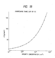
- Fig. 18 is a graph showing results of band-gap narrowing width calculations by using equation (2) when boron is doped in Si in a high concentration.
- the impurity density (cm ⁇ 3) is plotted along the abscissa in Fig. 8, and the narrowed width ⁇ E g (meV) of the band gap is plotted along the ordinate in Fig. 8.
- ⁇ E g ⁇ E gb - ⁇ E ge ⁇ 50 meV. Therefore, h FE ⁇ 7.4 h FE0 .
- the present invention has a great advantage in a base having a high impurity concentration.
- a p-type impurity has low solubility as compared with phosphorus (P) and arsenic (As) as n-type impurities.
- Fig.19 shows data of solubility of a solid-phase impurity in silicon. Temperatures (T °C) are plotted along the abscissa, and the solubility in the solid phase is plotted along the ordinate.
- P-type impurities are exemplified by B, Ga, and Al. Of these impurities, B can be dissolved the highest concentration. When the impurity is doped to exceed the degree of solid solution, the impurity is precipitated in Si during the manufacturing process of the semiconductor device to form crystal defects, thereby adversely affecting the BPT characteristics. However, this depends on process temperatures.
- B can be most stably doped to a high concentration and is most suitable as a p-type impurity.
- a tetrahedral atomic radius of the impurity in Si poses a problem. More specifically, since Si has a diamond type crystal structure, it has tetrahedral bonds. In this case, an atomic radius r presents a problem. If a difference between atomic radii is given as 100 x (r - r Si )/r Si , the difference for B can be given as about -25. Since the atomic radius of B is smaller than that of Si, a stress occurs between a boundary between the B-nondoped emitter and collector having an impurity concentration of 1018 cm ⁇ 3. When this stress is conspicuously increased, dislocation occurs. For this reason, electrical leakage occurs between the base-emitter path or the base-collector path, thereby decreasing a breakdown voltage. The current gain is also decreased.
- B and Ge are simultaneously doped in the base region.
- a value of 100 x (r GE - r Si )/r Si of Ge is almost +4. That is, the Ge value is larger than Si by 4%.
- the semiconductor device since the p-type base region is formed to have an impurity concentration distribution by, e.g., ion implantation, the semiconductor device has a structure in which lattice distortion tends not to occur.
- the Ge concentration is not limited to the one described above.
- the dose of B with respect to the base is continuously changed, and occurrence of defects and dislocation becomes difficult. Therefore, the defect occurrence limit of B has a peak concentration higher than the B concentration of 1018 cm ⁇ 3.
- the main purpose of doping Ge is to reduce a band gap smaller than that of Si upon doping of Ge into Si.
- the concentration which influences the band gap is not satisfied by 8.25 times that of B, but must be 1020 cm ⁇ 3 or more to obtain a satisfactory effect.
- Ge has a band gap smaller than that of Si.
- the band gap of Si is E gSi ⁇ 1.1 eV
- the band gap of Ge is E gGe ⁇ 0.7 eV.
- the Ge concentration is about 5 x 1021 cm ⁇ 3 and is 10 times or more the B concentration.
- Fig. 20 is a graph showing an effect to a Ge band gap.
- a composition ratio X is plotted along the abscissa, and changes in band gap E g , changes on the conduction band side ⁇ E c and the valence band side ⁇ E v in Fig. 20.
- the base band gap can be reduced. Therefore, the current gain of the BPT can be increased.
- Al, Ga, or the like may be used as a p-type impurity to be doped in the base.
- these p-type impurities have a value of 100 x (r - r Si )/r Si to be almost +8 and cannot correct lattice distortion of a substance having a small atomic radius.
- carbon (C) has a small atomic radius
- Si 1-X C X has a direction to increase a band gap. That is, Si 1-X C X has a property opposite to band-gap narrowing. Therefore, the combination of Si and C is not preferable.
- B and Ge is a best combination for a p-type base.
- the base consists of an Si-Ge-B mixed crystal
- injection of positive holes in the emitter can be suppressed, which does not a barrier for injection of electrons from the emitter to the base.
- the oxide film formed between the emitter region and the base region is removed, characteristic variations between the BPTs can be eliminated.
- the current gain h FE can be increased although any oxide film is not formed between the emitter region and the base region.
- the current gain h FE can be increased due to the following reason.
- J B ′ (q ⁇ n i 2 ⁇ D P /N E ⁇ L P ) x coth(W E /L P )[exp(V BE /kT)-1]
- V BE dependency of the current gain h FE can also be eliminated.
- the present inventors measured V BE dependency of the base current J B and the collector current J C of the conventional BPT described above.
- J B was almost proportional to exp(V BE /kT), but J C had a relation represented by J C ⁇ exp(V BE /nkT).
- the n value fell within the range of 1.01 to 1.05. That is, the n value was larger than the normal value by 1 to 5%.
- V BE dependency of h FE is caused by J C .
- This J C characteristic is expected such that the potential barrier on the conduction band side by an Si oxide film in the emitter region influences electron injection from the emitter to the base.
- V BE dependency of h FE greatly influences a ratio ( ⁇ value) of an optical input to an electrical output. This dependency becomes a decisive problem when semiconductor devices are to be manufactured uniformly.
- V BE dependency of h FE preferably falls within the range of 5%, condition ⁇ ⁇ 1.25 x 10 ⁇ 3 must be satisfied.
- the height of the potential barrier can be allowed to be about kT when, e.g, an n+-type emitter is formed.
- kT when the height of the potential barrier exceeds kT, an influence on the electrical characteristics cannot be neglected.
- a potential barrier of a valence band naturally poses a problem in an p+-type emitter.
- the carriers are conducted by a tunnel effect.
- the height of the potential barrier need not be kT or less.
- the potential barriers are not uniform in all regions. However, if the highest potential barrier is kT or less, no problem is posed.
- a conventional problem of a point defect or dislocation in a hetero interface between Si forming an emitter region and Si 1-X Ge X forming a base region can be solved, thereby reducing a base current and increasing a current gain h FE .
- the semiconductor device of the present invention Since the semiconductor device of the present invention has a high current gain as described above, it can increase a frequency f T . Therefore, when the semiconductor device of the present invention is adopted as a photoelectric transducer apparatus for use in a solid-state image pickup apparatus or the like, a read rate of the solid-state image pickup apparatus can be improved.
- an emitter is made of Si
- a base is made of Si 1-X Ge X .
- Analytically theoretical expressions of a base current and a collector current in a BPT of the present invention are as follows (note that the end of the emitter is brought into contact with a metal).
- h FE is uniquely determined by the value of (L N /W B ).
- the present invention is partly characterized in that the depth of Si 1-X Ge X is the same as or larger than that of the base. This feature of the present invention will be described in detail below.
- the Si 1-X Ge X layer and the p-type layer do not always coincide with each other.
- the Si 1-X Ge X layer can be formed in only a region shallower than the p-type layer from the surface, a problem is posed.
- a potential of the BPT is obtained as shown in Fig. 11. Referring to Fig. 11, a forward bias is applied is between the emitter and the base, and a reverse bias is applied between the base and the collector.
- the interface between Si 1-X Ge X and Si must be formed in the depletion layer of the base and collector junction or in the collector.
- the interface must be formed in the depletion layer of the emitter and the base or at the emitter side. In this manner, diffusion of the minority carriers injected from the base to the emitter can be interrupted by the barrier at the hetero interface. That is, the hetero interface between Si and Si 1-X Ge X must not be formed at a neutral region of a region serving as a base.
- an impurity distribution upon ion implantation by, e.g., an SIMS (secondary ion mass analyzer), ion implantation conditions can be easily determined.
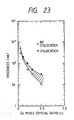
- Fig. 24 shows an analysis example obtained by the SIMS. Comparison is performed with respect to the SIMS analysis result in accordance with a designed mixed crystal ratio X, and the thickness of the heterojunction, i.e., the ion implantation conditions are determined in accordance with data shown in Fig.23.
- the mixed crystal ration X is a ratio between numbers of Si and Ge atoms. Since Si is substantially 5 x 1022 cm ⁇ 3, The ratio X can be easily calculated by a dose of Ge. That is, X is preferably 0.5 or less.
- I C is a collector current
- C be is a base-emitter capacitance
- C bc is a base-collector capacitance
- r EE is an emitter series resistance
- r CC is a collector series resistance
- ⁇ B is a base travel time
- ⁇ C is a travel time in a collector depletion layer.
- the resistance r EE is mostly caused by an ohmic contact and depends of a surface concentration and an electrode. That is, the surface need only be N++.
- r CC is influenced more by the thickness of an n ⁇ -type region 3 than those of n+-type regions denoted by reference numerals 2 and 7 shown in Fig. 25.
- f T is a time delay of carriers from the emitter to the collector.
- a inflection point determined by J1 is a point on which a high-current effect has an influence.
- ⁇ B W B 2/ ⁇ D B (7)
- ⁇ 2D B / ⁇ B W B
- ⁇ 0 kT/qW B
- ⁇ bi ⁇ V/W B
- a region in which the above equation is not satisfied corresponds to a transistor current drive limit.
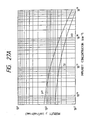
- J C ⁇ q(D n /W B )N D (15) obtained by substituting (n i 2/N B ) ⁇ (V BE + ⁇ E g )/kt ⁇ of equation (13) by an emitter concentration N D is a current drive limit for emitter concentration definition of this transistor.
- N C is 6.2 x 1015 cm ⁇ 3.
- J C is 1 x 10⁵ A/cm2
- N C is 6.2 x 1016 cm ⁇ 3.
- a current represented by J1 in Fig. 26 normally has this value.
- N C is 3 x 1016 cm ⁇ 3, ⁇ ec does not increase at a high rate untill 5 x 10⁴ A/cm2.
- a base impurity concentration will be described below.
- a base carrier concentration is good as long as the number of injected minority carriers is (n i 2/N B )exp ⁇ (V BE + ⁇ E g )/kT ⁇ or more. If the number is larger than this value, neutrality of a charge can be maintained. That is, assuming that a base impurity concentration is N B , the following relation need only be satisfied: N B » (n i 2/N B )exp ⁇ (V BE + ⁇ E g )/kT ⁇ (17) When N B becomes close to n i exp ⁇ (V BE + ⁇ E g )/2kT ⁇ , a space-charge effect appears, and a resistance in the base rises at a high rate.
- N C 3 x 1016 cm ⁇ 3
- W BC 0.35 ⁇ m
- ⁇ VC of equation (10) is 1.75 psec, thereby posing no problem.
- ⁇ B obtained from equation (7) indicates that at least W B must be 0.1 ⁇ m or less.
- X P is at least X P ⁇ W B .
- N B must be about 2 x 1017 cm ⁇ 3 or more.
- the emitter-base voltage is a bias value
- the base-collector voltage +5V
- C be 3.6 fF
- C bc 4.4 fF
- W BC 0.39 ⁇ m. Therefore, ⁇ vc and ⁇ c are sufficiently small.
- ⁇ e is basically in inverse proportion to I C and is vary small in a high-current region. Therefore, the lower limit of ⁇ ec is determined by the base travel time ⁇ B .
- ⁇ B determines the upper limit of f T .
- the hetero BPT of the present invention having a potential gradient can keep its high performance.
- the abscissa represents a distance standardized by a base width W B
- f T of a photoelectric transducer apparatus can be improved, and a nondestructive degree can be improved by increasing a current gain.
- a solid-state image pickup apparatus capable of reading data from the same element a plurality of times without performing correction and capable of performing high-speed reading.
- a semiconductor device having small characteristic variations, a high current gain h FE , and a high frequency, and a photoelectric transducer apparatus using the same.
- the oxide film formed at the interface between the base and the emitter can be eliminated, and the emitter region consists of single-crystal silicon.
- h FE J C (J B1 + J B2 ) (9)
- the diffusion current of positive holes from the base to the emitter is represented by equation (1).
- the diffusion length L p of the positive holes as minority carriers can be reduced, and J B1 is increased accordingly. Therefore, the current gain h FE is lowered.
- the emitter consists of single-crystal silicon according to the present invention.
- the diffusion length L p of positive holes serving as minority carriers in the emitter is increased. Therefore, the current gain h FE is increased as compared with the case wherein the emitter consists of polysilicon without an oxide film.
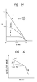
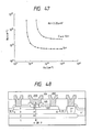
- Fig.30 is a graph illustrating V BE dependency of h FE .
- the current gain h FE is plotted along the ordinate, and the voltage V BE is plotted along the abscissa in Fig. 30.
- a region 1 is a current region generally represented by equations (1) to (3) and (9).
- a region 2 is a large-current region which cannot be represented by equations (1) to (3) and (9).
- the n value was about 1.01 to 1.05 for a thin silicon oxide film (10 to 30 ⁇ ) and was larger than a normal value by about 1 to 5%. For this reason, the current gain h FE depends on V BE . That is, this is the reason why V BE dependency of the current gain h FE can be eliminated by removing the thin silicon oxide film.
- the n value is large in the presence of the thin silicon oxide film because the potential barrier on the conduction band by the silicon oxide film seems to influence injection of electrons from the emitter to the base.
- n 1 + ⁇ ( ⁇ « 1)
- J B J B0 ⁇ exp(V BE /kT) (11)
- J C J C0 ⁇ exp ⁇ V BE /(1 + ⁇ )kT ⁇
- V BE dependency of h FE greatly influences an optical input vs. electrical output ratio ( ⁇ value). This dependency also presents a significant problem when elements are to be uniformly manufactured.
- a maximum height of this potential barrier can be allowed to about kT in a conduction band of an n+-type emitter. When the maximum height exceeds kT, electrical characteristics are adversely affected.
- the potential barrier of the valence band presents a significant problem in a p+-type emitter.
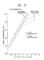
- Equations (14) and (15) can be established within the range of Boltzmann statistics. When an impurity density is high enough to be measured by Fermi-Dirac statistics, equations (14) and (15) cannot be used.
- the impurity concentration is 2.1 x 1019 cm ⁇ 3 for n-type, or 8 x 1018 cm ⁇ 3 for p-type.
- the alternate long and short dashed line in Fig. 3 exhibits a case obtained by using the Boltzmann statistics.
- the normalized energy is higher than -1, a difference between the Boltzmann statistics and the Fermi-Dirac statistics occurs. In this case, unless the Fermi-Dirac statistics is used, Fermi energy cannot be accurately evaluated.
- n- and p-type semiconductors The difference between the n- and p-type semiconductors is caused by different band structures and different effective masses. This value varies depending on the types of material.
- a region having a high impurity concentration of 1019 cm ⁇ 3 or more is formed on the emitter surface.
- the potential distribution is shown in Fig. 32, and a potential barrier ⁇ E B is formed in the emitter, as is apparent from Fig. 32.
- This potential barrier is formed by a Fermi level difference with respect to the carrier concentration, as shown in Fig.32.
- the positive holes injected from the base are blocked by this potential barrier. Therefore, the base current is reduced, and the current gain h FE can be increased.
- the impurity concentration is set to satisfy condition ⁇ E B > kT. If condition ⁇ E B > 2kT is satisfied, this effect is further enhanced.
- a current by recombination of positive holes injected from the base can be represented by equation (1), i.e., the same equation as obtained when the thin silicon oxide film is formed between the base and the emitter. In this case, if W E ′ « L p , then J B1 is decreased, and the h FE of the BPT can be increased.
- N E1 an impurity concentration within the emitter near the base
- N E2 an impurity concentration of the region having a high impurity concentration
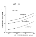
- inequality ⁇ E B ⁇ kT is derived from equation (14) under the following condition: N E2 > eN E1 (16) More accurately, N E1 and N E2 can be obtained by using the data shown in Fig. 3.
- Condition ⁇ E B ⁇ kT is equal to condition N E2 ⁇ eN E1 .
- W E ′ must satisfy condition 2W E ′ ⁇ L p so as to obtain a satisfactory effect.
- the current gain h FE can be increased.
- Equation (8) if the emitter impurity density is given as 1018 cm ⁇ 3 and the base impurity density is given as 1019 cm ⁇ 3, then ⁇ E gb - ⁇ E ge ⁇ 50 meV. Therefore, h FE ⁇ 74h FE0 can be obtained.
- B is preferably used as a base impurity.
- a p-type impurity has low solubility as compared with phosphorus (P) and arsenic (As) as n-type impurities.
- Fig. 19 shows data of solubility of a solid-phase impurity in silicon. Temperatures (T °C) are plotted along the abscissa, and the solubility in the solid phase is plotted along the ordinate.
- P-type impurities are exemplified by B, Ga, and Al. Of these impurities, B can be dissolved in the highest concentration. When the impurity is doped to exceed the degree of solid solution, the impurity is precipitated in Si during the manufacturing process of the semiconductor device to form crystal defects, thereby adversely affecting the BPT characteristics (note that this depends on process temperatures).
- B can be most stably doped up to a high concentration and is most suitable as a p-type impurity.
- Ge together with B is doped in the base.
- the purpose of Ge doping is...
- Ge together with B is doped in the base.
- the purpose of Ge doping is to narrow the band gap.
- the Ge concentration is preferably 8.25 times or more the B concentration due to the following reason.
- a tetrahedral atomic radius of the impurity in Si poses a problem. More specifically, since Si has a diamond type crystal structure, it has tetrahedral bonds. In this case, an atomic radius r presents a problem. If a difference between atomic radii is given as 100 x (r Ge - r Si )/r Si , the difference for B can be given as about -25.
- the atomic radius of Ge i.e., 100 x (r Ge - r Si )/r Si , is about +4. That is, the Ge value is larger than Si by 4%.
- the semiconductor device since the p-type base region is formed to have an impurity concentration distribution by, e.g., ion implantation, the semiconductor device has a structure in which lattice distortion tends not to occur.
- the Ge concentration is not limited to the one described above.
- the Ge dose is preferably 8.25 times or more the B dose.
- Al, Ga, or the like may be used as a p-type impurity to be doped in the base (however, these p-type impurities have 100 x (r - r Si )/r Si ⁇ +8) and cannot correct lattice distortion of a substance having a small atomic radius.
- carbon (C) has a small atomic radius
- Si 1-x C x has a direction to increase a band gap. That is, Si 1-x C x has a property opposite to band-gap narrowing. Therefore, the combination of Si and C is not preferable.
- B and Ge is a best combination for a p-type base.
- the lower limit value of the base concentration is determined by band tailing and is therefore given as 1 x 1018 cm ⁇ 3.
- the upper limit of the base concentration is about 1 x 10²⁰ since the solid solution limit shown in Fig. 19 is given.
- a p-n junction breakdown voltage is determined by avalanche amplification when the impurity concentration of an emitter region is 1017 cm ⁇ 1 or less. However, when the impurity concentration of the emitter region is 1017 cm ⁇ 3 or more, an influence of a tunnel current is enhanced. When the impurity concentration of the emitter region is 1018 cm ⁇ 3 or more, the breakdown voltage is determined by only a tunnel current.
- equation (18) is applied to silicon, it yields the following equation.
- J t 1.649 x 10⁴ ⁇ V ⁇ exp[-3.052 x 10⁹/ ⁇ ] (19)
- a base-emitter breakdown voltage is required to be at least 2 V.
- an emitter size is reduced (e.g., 3 x 3 ⁇ m2) and the emitter junction becomes shallow (0.5 ⁇ m or less)
- a current becomes larger than those given by equations (18) and (11) by an influence of currents near the emitter.
- the lower limit of the emitter impurity concentration will be described below.
- J C ⁇ (q ⁇ n i 2 ⁇ D n )/(N B ⁇ W B ) ⁇ exp(V BE /kT) (20)
- This equation is established within the range approximated by the minority carriers as follows: N D » (n i 2/N B )exp(V BE /kT) (21) (N D is the emitter impurity concentration)
- N D is the emitter impurity concentration
- the current drive limit of the prescribed emitter impurity concentration of this transistor is given by substituting (n i 2/N B )exp(V BE /kT) with the emitter concentration N D as follows: J C ⁇ q ⁇ (D n /W B ) ⁇ N D (22)
- the normal transistor requires J C of 1 x 10⁴ to 105 A/cm2.
- a base-emitter breakdown voltage is required to be at least 2 V.
- an emitter size is reduced (e.g., 3 x 3 ⁇ m2) and the emitter junction becomes shallow (0.5 ⁇ m or less)
- a current becomes larger due to an influence of currents near the emitter.
- the upper limit of the emitter impurity concentration will be described below.
- the emitter concentration is set to be 4.5 x 1018 cm ⁇ 3 or less for the base concentration of 1 x 1018 cm ⁇ 3.
- the base concentration is given as 5 x 1018 cm ⁇ 3
- the emitter concentration is set to be 1 x 1018 cm ⁇ 3 or less.
- the emitter concentration is set to be 9 x 1017 cm ⁇ 3 or less.
- the emitter concentration is set to be 4.5 x 1018 cm ⁇ 3 or less. This emitter concentration is the upper limit.
- the upper limit of the collector concentration is determined by the above breakdown voltage.
- a breakdown voltage in the emitter-collector (E-C) path of the BPT is determined by a base-collector (B-C) breakdown voltage when the base concentration is increased.
- the E-C breakdown voltage is required to be 10 V for a safe margin.
- the collector concentration is set to be N C ⁇ 1.5 x 1017 cm ⁇ 3.
- the breakdown voltage is required to be 6 V or more. Therefore, the collector impurity concentration N C is about 3 x 1017 cm ⁇ 3.
- the lower limit of the collector concentration is determined by the current limit.
- an acceleration electric field is applied to the base-collector junction.
- the collector impurity concentration can be about 6 x 1015 cm ⁇ 3 or more according to equation (25).
- the lower limit is not restricted to the above-mentioned lower limit.
- a base width is determined by an h FE requirement, the base width is not limited to a specific value.
- a cutoff frequency f T of the BPT will be described below.
- I C is a collector current
- C be is an emitter-base capacitance
- C bc is a base-collector capacitance
- r EE is an emitter series resistance
- r CC is a collector series resistance
- L B is a travel time in the base
- L C is a travel time in a collector depletion layer.
- the resistance r EE is a resistance given by almost ohmic contact and depends on a surface concentration and an electrode.
- the impurity concentration of the surface is preferably n++.
- ⁇ 2D B / ⁇ B W B .
- the travel time in the base is long because the carriers travel in the base by diffusion.
- the base and collector concentrations are determined so that W BC is set to be 1 ⁇ m or less.
- the base carrier concentration value need be larger than the number n12/N B exp(V BE + ⁇ E g /kT) of injected minority carriers. In this case, neutrality of the charges can be assured, that is, N B » n12/N B exp(V BE + ⁇ E g /kT) (33)
- a base-collector impurity density will be examined with reference to the width W BC of the base-collector deletion layer.
- W B Since W B must be 0.1 ⁇ m or less according to equation (27) when a voltage of 5 V is applied across the base-collector path, x p satisfies at least condition x p ⁇ W B .
- the concentration N B must be almost 2 x 1017 cm ⁇ 3 or more from Fig. 11.
- a BPT having an arrangement as shown in Fig. 35 is formed by using an ion implantation method.
- Fig. 36 is a graph showing impurity distributions and a Ge distribution at a portion indicated by A - A′ in Fig. 35.
- the abscissa represents a depth
- the ordinate represents impurity concentrations of Ge, P, and B. Note that the ordinate represents logarithmic values while the abscissa represents linear indications.
- Phosphorus (P) is an impurity in an emitter region
- B is an impurity in a base region
- Ge represents the concentration of Si 1-X Ge X in Si.
- P, B, and Ge does not always represent an absolute relationship.
- p and B are used as impurities.
- the impurities are not limited to those used in this embodiment.
- a relationship between the Ge peak value and the depth is uniquely determined by a relationship between the dose and the acceleration voltage.
- the thickness of a transition region between Si and Si 1-X Ge X is mainly determined by the acceleration voltage and annealing in the following process.
- An emitter-base junction surface (E-B surface) is preferably close to a Ge peak concentration.
- Exp( ⁇ E g /kT) represents an effect of the E-B heterojunction.
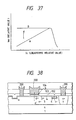
- FIG. 37 shows an improvement according to the present invention.
- A represents a conventional HBT; and B, an HBT of the present invention.
- X is preferably 0.5 or less. If X exceeds 0.5, it is difficult to manufacture a good BPT. In addition, X of 0.5 or less is sufficient in the BPT.
- a heterojunction having an inclined transition region can be formed without using ion implantation, ion implantation is preferably used.
- a heterojunction having an inclined transition region can be formed by a vapor-phase growth method.
- an H2 + SiH2Cl2 + GeH4-based gas for example, is used, and a gas concentration of GeH4 is continuously changed to form a base region.
- a temperature is 900°C or less
- a gas pressure is 100 Torr or less
- an epitaxial rate is 500 ⁇ /min
- the heterojunction is assumed to be obtained by an epitaxial technique in vacuum.
- Ion implantation is superior because a mixed crystal ratio can be stably set, a Ge concentration distribution can be correctly reproduced, and a mass production property is good.
- Si is in the form of amorphous after ion implantation of Ge, it can be easily subjected to solid-phase epitaxy, thereby reducing the temperature of a process. Furthermore, since a diffusion constant of Ge or Si is very small, the Ge concentration distribution does not almost change upon ion implantation in an annealing step at 1,000°C or less.
- a distribution function with respect to a depth direction X in a semiconductor upon ion implantation is approximated as follows: N(X) ⁇ (N o /2.5R P )exp(-(X-R P )2/( ⁇ R P peak position, and ⁇ R P is a distance from the peak to one diffusion amount (1 ⁇ ).
- R P and ⁇ R P are changed by an acceleration voltage.
- Fig. 38 shows another embodiment of the present invention.
- a hetero BPT according to this embodiment is the same as that of Embodiment 1 except that an emitter has a buried structure, a substrate 1 has an n conductivity type, and no buried region is formed.
- h FE can be increased as in the hetero BPT shown in Embodiment 1.
- Fig. 39 shows the third embodiment of the present invention.
- a hetero BPT according to this embodiment differs from Embodiment 1 in that an n+-type contact 8 is formed.
- the n+-type contact 8 is formed to reduce an ohmic resistance of an emitter 5.
- An impurity concentration of the n+-type contact 8 is preferably 1019 to 1021 cm ⁇ 3.
- h FE can be increased as in the hetero BPT shown in Embodiment 1.
- Fig. 40 shows an embodiment in which an emitter 5 is formed on a substrate.
- h FE can be increased.
- Fig. 41 is a circuit diagram showing a case in which the hetero BPT shown in the first embodiment is applied to a solid-state image pickup apparatus in Patent Application (2) filed by the present applicant on December 21, 1987.
- the hetero BPT shown in Embodiment 1 is used in a portion indicated by Tr.
- the hetero BPT is used as a photoelectric transducer element.
- the present invention can improve f T (frequency) of a semiconductor device, the present invention is very effective when it is applied to a photoelectric transducer apparatus.
- F T is determined by a read rate.
- a current photoelectric transducer apparatus has 500 x 640 elements.
- An HD High Division: an area sensor corresponding to a high vision
- An HD has 1,000 x 2,000 elements.
- a horizontal scanning period HT ⁇ 50 ⁇ sec, and a horizontal blanking period HALK is 8 to 10 ⁇ sec.
- HT 3 to 3.7 ⁇ sec
- HBLK 26 ⁇ sec.
- a frequency must be at least six times that of a current television. That is, since a frequency is currently f T ⁇ 1 to 2 GHz, f T > 6 to 16 GHz.
- ⁇ E g is preferably 0.15 eV or less.
- optical information of the same photoelectric transducer element is read a plurality of times. Since information is read from the same element a plurality of times, a ratio between electrical outputs upon first reading and reading from the second time is important. If this value is reduced, correction must be performed.
- the ratio between the first and second read outputs is defined as a nondestructive degree.
- Nondestructive degree (C tot x h FE )/(C tot x h FE + C V )
- C tot is a total capacitance connected to the bases of the photoelectric transducer elements indicated by Tr in Fig. 7 and is determined by a base-emitter capacitance C be , a base-collector capacitance C bc , and C ox .
- C V is a stray capacitance of read lines represented by VL1... VL n . Note that C ox is not present depending on circuit systems.
- the nondestructive degree can be easily improved by increasing h FE . That is, when h FE is increased, the nondestructive degree can be increased.
- h FE is about 1,000. Therefore, no sufficient nondestructive degree can be obtained. In the semiconductors device of the present invention, however, a high nondestructive degree is obtained since h FE can be sufficiently increased.
- the nondestructive degree is more preferably 0.98 or more.
- h FE must be about 10,000. This value cannot be achieved by a conventional hetero BPT or homo BPT. That is, this value can be achieved by only the hetero BPT of the present invention.
- the present invention can be applied to a line sensor.
- the present invention since a heterojunction having an inclined transition region is formed in an interface between an Si 1-X Ge X mixed crystal and Si of a semiconductor device, the number of point defects and dislocations can be significantly reduced. Therefore, a current gain can be significantly improved in a region having a very small collector current.
- an ion implantation method is used. Therefore, a semiconductor device can be very easily manufactured and mass production can be facilitated.
- Embodiments 1 - 5 a high-performance semiconductor device and a photoelectric transducer apparatus using the same can be provided at very low cost.
- a BPT having the same structure as in Fig. 42 was manufactured as an embodiment of the present invention by using an ion doping method.
- the above general steps constitute the manufacturing process of this embodiment.
- the most important step in this embodiment is step 5, i.e., the base formation step.
- the ion implantation method has advantages in that a mixed crystal can be stably set, the Ge concentration distribution can be accurately reproduced, and mass production can be facilitated.
- Si is amorphous, and solid-phase epitaxial growth can be easily performed. Therefore, a low-temperature process can be performed.
- Ge has a small diffusion constant in Si and an advantage in that the Ge concentration distribution at the time of ion implantation is rarely changed when annealing is performed at 1,000°C or less.
- a distribution function of the semiconductor in a direction X of depth during ion implantation can be approximated as follows: N(X) ⁇ (N o /2.5R p ) exp(-(X-R p )2/( ⁇ R p )2) (18) where N o is an implantation amount per unit area, R p is a peak position, and ⁇ R p is a distance at which an implantation amount is reduced to one diffusion amount (1 ⁇ ) from the peak. The position R p and the distance ⁇ R p are changed in accordance with an acceleration voltage.
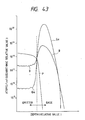
- Fig. 43 is a graph showing B, Ge, and P distributions when ion implantation is performed as described above.
- the depth (relative value) is plotted along the abscissa, and the atomic number/cm ⁇ 3 is plotted along the ordinate in Fig. 43.
- a semiconductor device having a high base-emitter breakdown voltage, a small base-emitter capacitance, and a high h FE .
- Fig. 44 is a view showing another embodiment of the present invention.
- a hetero BPT according to this embodiment is different from that of Embodiment 6 except that an emitter has a buried structure, a substrate 1 has an n conductivity type, and a buried region is eliminated.
- Fig. 45 shows a structure wherein an emitter region 5 is formed on a substrate 1 side.
- Fig. 46 is a view showing the 8th embodiment of the present invention.
- a hetero BPT of this embodiment is different from that of Embodiment 6 except that an n+-type contact 8 is formed.
- the n+-type contact 8 is formed to decrease an ohmic resistance of an emitter 5.
- the n+-type contact 8 has an impurity concentration of 1020 cm ⁇ 3.
- Fig. 41 is a circuit diagram wherein the BPT shown in Embodiment 6 is used in a solid-state image pickup apparatus.
- the BPT shown in Embodiment 6 is used in a portion represented by Tr in Fig. 41.
- the BPT shown in Embodiment 6 is used as a photoelectric transducer element.
- f T (frequency) of the semiconductor device can be increased. Therefore, when the semiconductor device is used in the photoelectric transducer apparatus, it is very effective.
- the frequency f T in the photoelectric transducer apparatus is determined by a read rate.
- An existing photoelectric transducer apparatus has 500 x 640 elements.
- An HD High Diffusion; an area sensor corresponding to high vision
- An HD High Diffusion; an area sensor corresponding to high vision
- a horizontal scan period is HT ⁇ 50 ⁇ sec, and a horizontal blanking period HALK is 8 to 10 ⁇ sec.
- HT 3 to 3.7 ⁇ sec
- HBLK 26 ⁇ sec.
- the frequency is required to be at least six times. That is, in the existing scheme, f T ⁇ 1 to 2 GHz. Therefore, f T > 6 to 16 GHz or more is required.
- the ratio of the first read output to the second read output is defined as a nondestructive degree.
- the nondestructive degree is represented by the following equation.
- Nondestructive Degree (C tot x h FE )/(C tot x h FE + C V )
- C tot is a total capacitance connected to the bases of the photoelectric transducer elements represented by Tr in Fig. 41.
- the total capacitance C tot is determined by a base-emitter capacitance C be , a base-collector capacitance C bc , and C 0x .
- C V is a stray capacitance of read lines represented by VL1... VL n . Note that C ox is not present depending on circuit systems.
- the nondestructive degree can be easily improved by increasing the current gain h FE . That is, when h FE is increased, the nondestructive degree can be increased.
- C V is a stray capacitance of vertical lines
- N B 1019 cm ⁇ 3
- 6.3 x 1017 cm ⁇ 3 for C be 5fF.
- h FE is about 1,000 in a conventional homo BPT, a sufficiently high nondestructive degree could not be obtained.
- a sufficient high h FE can be obtained, an excellent nondestructive degree can be obtained.
- the nondestructive degree is 0.98 or more.
- h FE must be about 10,000. In the conventional homo BPT, this value cannot be obtained but can be obtained by only the BPT of the present invention.
- the above embodiment exemplifies an area sensor, but the present invention is also applicable to a line sensor.
- the impurity concentration of the emitter can be suppressed to be 1019 cm ⁇ 3 or less. Therefore, band-gap narrowing can be suppressed, and efficiency of injection from the emitter can be improved.
- a band-gap narrowing effect obtained by a high boron concentration of the base and a mixed crystal effect obtained by using B together with Ge can cause to decrease a base band gap smaller than the emitter band gap. Therefore, the h FE of the BPT can be increased. In addition, the lattice distortion can be moderated, and therefore, defects at the interface can be minimized.
- Fig. 48 is a view showing a semiconductor device according to an embodiment of the present invention.
- the same reference numerals as in Fig. 4 denote the same parts in Fig. 48.
- the semiconductor device of this embodiment is different from the semiconductor device of Fig. 4 in that an emitter region 5 is formed by growing a single crystal by epitaxial techniques or the like and the oxide 102 is not formed between a base region 4 and the emitter region 5.
- a manufacturing process of the BPT of this embodiment is shown below.
- steps 8 and 9 which represent the manufacturing process of the emitter region.
- steps 8 and 9 which represent the manufacturing process of the emitter region.
- Single-crystal silicon can be grown by an epitaxial method using SiH4, Si2H6, SiCl4, SiHCl3, or SiH3Cl gas and a carrier gas.
- the Si surface must be cleaned beforehand by a gas mixture of H2 gas or HCl gas, or a gas mixture of a halogen gas such as HBr or HF.
- Cleaning and crystal growth can be performed at a low temperature and a low pressure of 10 to 100 Torr. The lower the temperature of cleaning and crystal growth is, the higher the packing density is.
- Surface cleaning can be performed by sputtering of a gas (e.g., Ar) or heating. In epitaxial growth, it is very important to perform perfect surface cleaning.
- a gas e.g., Ar
- the oxide film on the base region 4 must be removed. Although it is difficult to perfectly remove the oxide film, more perfect epitaxial growth can be performed in a smaller content of oxygen contained in the base surface.
- the current gain h FE of the resultant BPT was measured, and a higher gain than the conventional BPT could be obtained.
- Fig. 50 shows another embodiment of the present invention.
- a BPT of this embodiment is different from Embodiment 11 except that an emitter has a buried structure.
- an end portion of an emitter region 5 in the BPT of Embodiment 11 is deposited on the oxide film (insulator 102), the substance on the oxide film is polysilicon.
- the entire emitter region 5 consists of a single crystal, and the current gain h FE can be further increased. (Embodiment 13)
- Fig. 51 is a view showing the embodiment 13 of the present invention.
- This embodiment exemplifies a BPT in which an element isolation region is a groove isolation structure.
- the current gain h FE of this BPT can also be increased.
- Fig. 41 is a circuit diagram wherein the BPT of the embodiment 11 is used in a solid-state image pickup apparatus. Referring to Fig. 41, the BPT shown in Embodiment 11 is used in a portion represented by Tr.
- the BPT is used as a photoelectric transducer element.
- Nondestructive Degree (C tot x h FE )/(C tot x h FE + C V )
- C tot is a total capacitance connected to the bases of the photoelectric transducer elements represented by Tr in Fig. 4.
- the total capacitance C tot is determined by a base-emitter capacitance C be , a base-collector capacitance C bc , and C ox .
- C V is a stray capacitance of read lines represented by VL1... VL n . Note that C ox is not present depending on circuit systems.
- the nondestructive degree can be easily improved by increasing the current gain h FE . That is, when h FE is increased, the nondestructive degree can be increased.
- This embodiment exemplifies an area sensor.
- the present invention is also applicable to a line sensor.
- the current gain h FE can be higher than that of the conventional structure although the oxide film is not formed between the emitter and base regions.
- a BPT having an arrangement as shown in Fig. 35 is formed by using an ion implantation method.
- Fig. 24 is a graph showing impurity distributions and a Ge distribution at a portion indicated by A-A′ in Fig. 35.
- the abscissa represents a depth
- the ordinate represents impurity concentrations of Ge, P, and B.
- the ordinate represents logarithmic values while the abscissa represents linear indications.
- arsenic (As) is an impurity of an emitter region
- B is an impurity of a base region
- Ge represents the concentration of Si 1-X Ge X in Si.
- As, B, and Ge does not always represent an absolute relationship.
- As and B are used as impurities.
- the impurities are not limited to those used in this embodiment.
- a relationship between the Ge peak value and the depth is uniquely determined by a relationship between the dose and the acceleration voltage.
- the thickness of a transition region between Si and Si 1-X Ge X is mainly determined by the acceleration voltage and annealing in the following process.
- An emitter-base junction surface (E-B surface) is preferably close to a Ge peak concentration.
- exp( ⁇ E g /kT) is an effect of an E-B heterojunction.
- a base current is determined by a recombination current J Brec of electrons from an emitter and an injection current J Binj from a base to the emitter.
- Fig. 3 shows an improvement according to the present invention. Referring to Fig. 3, A represents a conventional HBT; and B, an HBT of the present invention.
- X is preferably 0.5 or less. If X exceeds 0.5, it is difficult to manufacture a good BPT. In addition, X of 0.5 or less is sufficient in the BPT.
- a heterojunction having an inclined transition region can be formed without using ion implantation, ion implantation is preferably used.
- a heterojunction having an inclined transition region can be formed by a vapor-phase growth method.
- an H2 + SiH2Cl2 + GeH4-based gas for example, is used, and a gas concentration of GeH4 is continuously changed to form a base region.
- a temperature is 900°C or less
- a gas pressure is 100 Torr or less
- an epitaxial rate is 500 ⁇ /min
- the heterojunction is assumed to be obtained by an epitaxial technique in vacuum.
- Ion implantation is superior because a mixed crystal ratio can be stably set, a Ge concentration distribution can be correctly reproduced, and a mass production property is good.
- Si is in the form of amorphous after ion implantation of Ge, it can be easily subjected to solid-phase epitaxy, thereby reducing the temperature of a process. Furthermore, since a diffusion constant of Ge or Si is very small, the Ge concentration distribution does not almost change upon ion implantation in an annealing step at 1,000°C or less.
- a distribution function with respect to a depth direction X in a semiconductor upon ion implantation is approximated as follows: N(X) ⁇ (N o /2.5R P )exp(-(X-R P )2/( ⁇ R P ) diffusion amount (1 ⁇ ).
- R P and ⁇ R P are changed by an acceleration voltage.
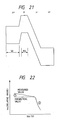
- Fig. 52 is a potential view of a BPT according to this embodiment.
- the band gap is E g ⁇ (E g ′ > E g ⁇ ).
- the drift effect is significant within the range of ⁇ E g2 > kT/q. Since kT/q is 0.025 eV at room temperature, an effect is obtained if the value is larger than that (i.e., a transit velocity V is increased). This effect becomes significant at a lower temperature. When the transit velocity V is increased, carriers in the base move rapidly to improve RF characteristics. In addition, in a drift structure, a moving velocity is not influenced by an operation temperature of a BPT.
- Fig. 53 shows the embodiment 17 of the present invention.
- a hetero BPT according to this embodiment is the same as that of Embodiment 1 except that an emitter has a buried structure, a substrate 1 has an n conductivity type, and no buried region is formed.
- hFE can be increased as in the hetero BPT shown in Embodiment 16.
- Fig. 54 shows an embodiment in which an emitter 5 is formed on a substrate.
- h FE can be increased as in the hetero BPT of Embodiment 16.
- Fig. 41 is a circuit diagram showing a case in which the hetero BPT shown in the first embodiment is applied to a solid-state image pickup apparatus. Referring to Fig. 41, the hetero BPT shown in Embodiment 16 is used in a portion indicated by Tr.
- the hetero BPT is used as a photoelectric transducer element.
- the present invention can improve f T (frequency) of a semiconductor device, the present invention is very effective when it is applied to a photoelectric transducer apparatus.
- f T is determined by a read rate.
- a current photoelectric transducer apparatus has 500 x 640 elements.
- An HD High Division: an area sensor corresponding to a high vision
- An HD has 1,000 x 2,000 elements.
- a horizontal scanning period HT ⁇ 50 ⁇ sec, and a horizontal blanking period HALK is 8 to 10 ⁇ sec.
- HT 3 to 3.7 ⁇ sec
- HBLK 26 ⁇ sec.
- a frequency must be at least six times that of a current television. That is, since a frequency is currently f T ⁇ 1 to 2 GHz, f T > 6 to 16 GHz.
- ⁇ E g is preferably 0.15 eV or less.
- optical information of the same photoelectric transducer element is read a plurality of times. Since information is read from the same element a plurality of times, a ratio between electrical outputs upon first reading and reading from the second time is important. If this value is reduced, correction must be performed.
- the ratio between the first and second read outputs is defined as a nondestructive degree.
- Nondestructive degree (C tot x h FE )/(C tot x h FE + C V )
- C tot is a total capacitance connected to the bases of the photoelectric transducer elements indicated by Tr in Fig. 41 and is determined by a base-emitter capacitance C be , a base-collector capacitance C bc , and C ox .
- C V is a stray capacitance of read lines represented by VL1... VL n . Note that C ox is not present depending on circuit systems.
- the nondestructive degree can be easily improved by increasing h FE . That is, when h FE is increased, the nondestructive degree can be increased.
- h FE is about 1,000. Therefore, no sufficient nondestructive degree can be obtained. In the semiconductor device of the present invention, however, a high nondestructive degree is obtained since h FE can be sufficiently increased.
- the nondestructive degree is more preferably 0.98 or more.
- h FE must be about 10,000. This value cannot be achieved by a conventional hetero BPT or homo BPT. That is, this value can be achieved by only the hetero BPT of the present invention.
- the present invention can be applied to a line sensor.
- a semiconductor device can be very easily manufactured to maintain a good mass production property.
- a high-performance semiconductor device and a photoelectric transducer apparatus using the same can be provided at very low cost.
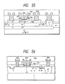
- Fig. 55 is a schematic sectional view showing a semiconductor device according to an embodiment of the present invention.
- the same reference numerals as in Fig. 6 denote the same parts in Fig. 55.
- the semiconductor device of this embodiment differs from the convention semiconductor device in the following points.
- the BPT shown in Fig. 55 was manufactured by the above steps.
- the most important steps in the present invention are step 6 of forming the base, step 7 of forming the single-crystal emitter, and step 8 of forming an impurity distribution the emitter. These steps will be described in more detail below.
- Step 6 of forming the base has effects wherein the shallow base is formed by forming a pre-amorphous base region upon ion implantation of Ge, and crystallization can be achieved upon doping of Ge.
- the base In order to obtain a high-speed BPT, the base must have a high impurity concentration and must be shallow.
- step 7 of forming the emitter when a thin oxide film is formed on underlying silicon, good single-crystal silicon cannot be deposited.
- the natural oxide film is removed by a reduction action in a low-pressure H2 atmosphere.
- surface cleaning may be performed by sputtering or the like using element ions in an HF gas or in a vacuum.
- film formation may be plasma CVD, CVD by sputtering, or the like. It is very important to suppress impurity diffusion from the base to the emitter during film formation. If the process is performed at 900°C or less, this diffusion can be sufficiently suppressed.
- step 8 of forming the impurity distribution in the emitter as a method of forming a region (LO) having a low impurity concentration and an surface area (HI) having a high impurity concentration from the emitter-base junction, an impurity doping method, annealing, or the like may be utilized to form the distribution.
- Deposition of emitter Si, the impurity distribution, impurity activation, and the like can be performed by low-temperature annealing (less than about 900°C) or a rapid annealing (e.g., lamp annealing and laser annealing).
- Fig. 56 shows another embodiment of the present invention.
- Embodiment 19 This embodiment is different from Embodiment 19 except that an emitter is embedded in an insulating film 102.
- the characteristics of the BPT of this type were evaluated, and the same characteristics as in the BPT of Embodiment 19 could be exhibited.
- a photoelectric transducer apparatus using the BPT of Embodiment 19 will be described as the embodiment 21 of the present invention.
- Fig. 57 is a schematic circuit diagram of the photoelectric transducer apparatus of this embodiment.
- This embodiment exemplifies a line sensor in which sensors S (S1, S2, 7) are aligned linearly.
- Each sensor S consists of a bipolar transistor and a reset transistor Q res connected to the base of the bipolar transistor. Carriers excited by light incident on the base of the bipolar transistor are accumulated and are read to the emitter. The reset transistor Q res is turned on to reset the bipolar transistor to a predetermined potential.
- a predetermined positive voltage is kept applied to the collector electrode of each sensor S, and emitter electrodes of the respective sensors S are connected to vertical lines L (L1, L2, ).
- a predetermined voltage V is applied to each vertical line through a transistor Q vrs , and a pulse ⁇ vrs for controlling the ON/OFF operation is input to the gate electrode of the transistor Q vrs .
- Each vertical line L is connected to an accumulation capacitor C t , and a signal is output from a transistor BPT2 through the transistor Q t .
- Fig. 41 is a circuit diagram in which the BPT shown in the embodiment 19 is used in a solid-state image pickup apparatus.
- the BPT shown in Embodiment 19 is used in a portion represented by Tr.
- the BPT is used as a photoelectric transducer element.
- Nondestructive Degree (C tot x h FE )/(C tot x h FE + C V ) (30)
- C tot is a total capacitance connected to the bases of the photoelectric transducer elements represented by Tr in Fig. 14.
- the total capacitance C tot is determined by a base-emitter capacitance C be , a base-collector capacitance C bc and C ox .
- C V is a stray capacitance of read lines represented by VL1... VL n . Note that C ox is not present depending on circuit systems.
- the nondestructive degree can be easily improved by increasing the current gain h FE . That is, when h FE is increased, the nondestructive degree can be increased.
- the current gain and the frequency characteristics of the semiconductor device can be greatly improved.
Landscapes
- Bipolar Transistors (AREA)
- Light Receiving Elements (AREA)
Applications Claiming Priority (10)
| Application Number | Priority Date | Filing Date | Title |
|---|---|---|---|
| JP312726/88 | 1988-12-10 | ||
| JP63312726A JP2664747B2 (ja) | 1988-12-10 | 1988-12-10 | 半導体装置およびこれを用いた光電変換装置 |
| JP63312725A JP2670118B2 (ja) | 1988-12-10 | 1988-12-10 | 半導体装置およびこれを用いた光電変換装置 |
| JP312725/88 | 1988-12-10 | ||
| JP77441/89 | 1989-03-29 | ||
| JP1077441A JP2768970B2 (ja) | 1989-03-29 | 1989-03-29 | 半導体装置およびこれを用いた光電変換装置 |
| JP1077439A JPH02256240A (ja) | 1989-03-29 | 1989-03-29 | 半導体装置およびこれを用いた光電変換装置 |
| JP77439/89 | 1989-03-29 | ||
| JP1079932A JP2559842B2 (ja) | 1989-03-30 | 1989-03-30 | 半導体装置およびこれを用いた光電変換装置 |
| JP79932/89 | 1989-03-30 |
Publications (2)
| Publication Number | Publication Date |
|---|---|
| EP0373832A2 true EP0373832A2 (fr) | 1990-06-20 |
| EP0373832A3 EP0373832A3 (fr) | 1992-03-18 |
Family
ID=27524668
Family Applications (1)
| Application Number | Title | Priority Date | Filing Date |
|---|---|---|---|
| EP19890312814 Withdrawn EP0373832A3 (fr) | 1988-12-10 | 1989-12-08 | Dispositif semi-conducteur et appareil de conversion photo-électrique l'utilisant |
Country Status (2)
| Country | Link |
|---|---|
| US (2) | US5159424A (fr) |
| EP (1) | EP0373832A3 (fr) |
Cited By (3)
| Publication number | Priority date | Publication date | Assignee | Title |
|---|---|---|---|---|
| US5302841A (en) * | 1990-11-28 | 1994-04-12 | Nec Corporation | Heterojunction bipolar transistor |
| US5422502A (en) * | 1993-12-09 | 1995-06-06 | Northern Telecom Limited | Lateral bipolar transistor |
| RU2477413C1 (ru) * | 2009-05-29 | 2013-03-10 | Вавин Б.В. | Разъединяющее приспособление для трубного пуш-фитинга |
Families Citing this family (22)
| Publication number | Priority date | Publication date | Assignee | Title |
|---|---|---|---|---|
| EP0373832A3 (fr) * | 1988-12-10 | 1992-03-18 | Canon Kabushiki Kaisha | Dispositif semi-conducteur et appareil de conversion photo-électrique l'utilisant |
| US6404003B1 (en) | 1999-07-28 | 2002-06-11 | Symetrix Corporation | Thin film capacitors on silicon germanium substrate |
| KR100275544B1 (ko) * | 1995-12-20 | 2001-01-15 | 이계철 | 선택적 컬렉터 박막 성장을 이용한 초자기정렬 바이폴러 트랜지스터의 제조방법 |
| JP2748917B2 (ja) * | 1996-03-22 | 1998-05-13 | 日本電気株式会社 | 半導体装置 |
| DE69941446D1 (de) * | 1998-04-09 | 2009-11-05 | Nxp Bv | Halbleiter mit gleichrichtendem übergang und seine herstellung |
| US6336084B1 (en) * | 1999-05-11 | 2002-01-01 | Ford Global Technologies, Inc. | Three-way catalyst model for an engine air-to-fuel ratio control system |
| US6995068B1 (en) * | 2000-06-09 | 2006-02-07 | Newport Fab, Llc | Double-implant high performance varactor and method for manufacturing same |
| US6362065B1 (en) * | 2001-02-26 | 2002-03-26 | Texas Instruments Incorporated | Blocking of boron diffusion through the emitter-emitter poly interface in PNP HBTs through use of a SiC layer at the top of the emitter epi layer |
| US6426265B1 (en) | 2001-01-30 | 2002-07-30 | International Business Machines Corporation | Incorporation of carbon in silicon/silicon germanium epitaxial layer to enhance yield for Si-Ge bipolar technology |
| JP2003168794A (ja) * | 2001-11-30 | 2003-06-13 | Canon Inc | 放射線検出素子、放射線撮像装置、放射線検出方法、及び放射線撮像方法 |
| US6656809B2 (en) | 2002-01-15 | 2003-12-02 | International Business Machines Corporation | Method to fabricate SiGe HBTs with controlled current gain and improved breakdown voltage characteristics |
| JP3565274B2 (ja) * | 2002-02-25 | 2004-09-15 | 住友電気工業株式会社 | バイポーラトランジスタ |
| US6893931B1 (en) * | 2002-11-07 | 2005-05-17 | Newport Fab, Llc | Reducing extrinsic base resistance in an NPN transistor |
| JP3959695B2 (ja) * | 2003-01-14 | 2007-08-15 | 松下電器産業株式会社 | 半導体集積回路 |
| US7011590B2 (en) * | 2003-07-08 | 2006-03-14 | Shimano, Inc. | Shift assist apparatus for a bicycle transmission |
| KR100781905B1 (ko) * | 2006-10-25 | 2007-12-04 | 한국전자통신연구원 | 헤테로 정션 바이폴라 트랜지스터를 포함하는 이미지 센서및 그 제조 방법 |
| JP5400280B2 (ja) * | 2007-06-07 | 2014-01-29 | パナソニック株式会社 | 固体撮像装置 |
| KR20120034965A (ko) | 2010-10-04 | 2012-04-13 | 삼성전자주식회사 | 태양 전지 |
| US10011920B2 (en) | 2011-02-23 | 2018-07-03 | International Business Machines Corporation | Low-temperature selective epitaxial growth of silicon for device integration |
| US9059212B2 (en) | 2012-10-31 | 2015-06-16 | International Business Machines Corporation | Back-end transistors with highly doped low-temperature contacts |
| US8912071B2 (en) * | 2012-12-06 | 2014-12-16 | International Business Machines Corporation | Selective emitter photovoltaic device |
| US11264526B1 (en) * | 2019-03-27 | 2022-03-01 | Hrl Laboratories, Llc | Infrared photodetector with optical amplification and low dark current |
Family Cites Families (18)
| Publication number | Priority date | Publication date | Assignee | Title |
|---|---|---|---|---|
| US3211970A (en) * | 1957-05-06 | 1965-10-12 | Rca Corp | Semiconductor devices |
| US3275906A (en) * | 1962-08-20 | 1966-09-27 | Nippon Electric Co | Multiple hetero-layer composite semiconductor device |
| US4467519A (en) * | 1982-04-01 | 1984-08-28 | International Business Machines Corporation | Process for fabricating polycrystalline silicon film resistors |
| US4633287A (en) * | 1982-08-09 | 1986-12-30 | Semiconductor Energy Laboratory Co., Ltd. | Semiconductor photoelectric conversion device |
| JPS5988875A (ja) * | 1982-11-12 | 1984-05-22 | Toshiba Corp | 光電変換素子 |
| US4672413A (en) * | 1984-04-16 | 1987-06-09 | Trw Inc. | Barrier emitter transistor |
| US4716445A (en) * | 1986-01-17 | 1987-12-29 | Nec Corporation | Heterojunction bipolar transistor having a base region of germanium |
| US4771326A (en) * | 1986-07-09 | 1988-09-13 | Texas Instruments Incorporated | Composition double heterojunction transistor |
| US4771013A (en) * | 1986-08-01 | 1988-09-13 | Texas Instruments Incorporated | Process of making a double heterojunction 3-D I2 L bipolar transistor with a Si/Ge superlattice |
| JPS63116465A (ja) * | 1986-11-05 | 1988-05-20 | Fujitsu Ltd | バイポ−ラトランジスタ |
| JPS63184364A (ja) * | 1987-01-27 | 1988-07-29 | Toshiba Corp | 半導体装置の製造方法 |
| GB8708926D0 (en) * | 1987-04-14 | 1987-05-20 | British Telecomm | Bipolar transistor |
| US4825259A (en) * | 1988-02-03 | 1989-04-25 | Berry Jr Robert F | Adapter tip for remote measuring device |
| EP0373832A3 (fr) * | 1988-12-10 | 1992-03-18 | Canon Kabushiki Kaisha | Dispositif semi-conducteur et appareil de conversion photo-électrique l'utilisant |
| JP2664747B2 (ja) * | 1988-12-10 | 1997-10-22 | キヤノン株式会社 | 半導体装置およびこれを用いた光電変換装置 |
| US4951115A (en) * | 1989-03-06 | 1990-08-21 | International Business Machines Corp. | Complementary transistor structure and method for manufacture |
| US5140400A (en) * | 1989-03-29 | 1992-08-18 | Canon Kabushiki Kaisha | Semiconductor device and photoelectric converting apparatus using the same |
| US5245204A (en) * | 1989-03-29 | 1993-09-14 | Canon Kabushiki Kaisha | Semiconductor device for use in an improved image pickup apparatus |
-
1989
- 1989-12-08 EP EP19890312814 patent/EP0373832A3/fr not_active Withdrawn
- 1989-12-08 US US07/448,211 patent/US5159424A/en not_active Expired - Fee Related
-
1994
- 1994-11-23 US US08/348,073 patent/US5691546A/en not_active Expired - Fee Related
Cited By (3)
| Publication number | Priority date | Publication date | Assignee | Title |
|---|---|---|---|---|
| US5302841A (en) * | 1990-11-28 | 1994-04-12 | Nec Corporation | Heterojunction bipolar transistor |
| US5422502A (en) * | 1993-12-09 | 1995-06-06 | Northern Telecom Limited | Lateral bipolar transistor |
| RU2477413C1 (ru) * | 2009-05-29 | 2013-03-10 | Вавин Б.В. | Разъединяющее приспособление для трубного пуш-фитинга |
Also Published As
| Publication number | Publication date |
|---|---|
| US5691546A (en) | 1997-11-25 |
| US5159424A (en) | 1992-10-27 |
| EP0373832A3 (fr) | 1992-03-18 |
Similar Documents
| Publication | Publication Date | Title |
|---|---|---|
| EP0373832A2 (fr) | Dispositif semi-conducteur et appareil de conversion photo-électrique l'utilisant | |
| US5708281A (en) | Semiconductor device and photoelectric conversion apparatus using the same | |
| US6049098A (en) | Bipolar transistor having an emitter region formed of silicon carbide | |
| US5557118A (en) | Hetero-junction type bipolar transistor | |
| US4958208A (en) | Bipolar transistor with abrupt potential discontinuity in collector region | |
| US5028973A (en) | Bipolar transistor with high efficient emitter | |
| EP0390521B1 (fr) | Transistor bipolaire et appareil de conversion photoélectrique utilisant le transistor bipolaire | |
| EP0551185A2 (fr) | Transistor bipolaire à hétérojonction | |
| US20070018192A1 (en) | Devices incorporating heavily defected semiconductor layers | |
| US5869851A (en) | Photoelectric conversion device with graded band gap and carrier concentration | |
| EP0327122B1 (fr) | Dispositif semi-conducteur complémentaire bipolaire | |
| EP0246700B1 (fr) | Transistors à porteurs de charge chauds | |
| EP0247667B1 (fr) | Transistors à porteurs de charge chauds | |
| JP2768970B2 (ja) | 半導体装置およびこれを用いた光電変換装置 | |
| JP2670118B2 (ja) | 半導体装置およびこれを用いた光電変換装置 | |
| EP0116652B1 (fr) | Phototransistor | |
| JP2915058B2 (ja) | 半導体装置および該装置を用いた光電変換装置 | |
| JP3145694B2 (ja) | 半導体装置 | |
| EP0431835B1 (fr) | Dispositif semi-conducteur bipolaire | |
| US6320211B1 (en) | Semiconductor device and electronic device by use of the semiconductor | |
| JP2664747B2 (ja) | 半導体装置およびこれを用いた光電変換装置 | |
| JP2770583B2 (ja) | コレクタトップ型ヘテロ接合バイポーラトランジスタの製造方法 | |
| JPH061783B2 (ja) | 半導体装置 | |
| JP2559842B2 (ja) | 半導体装置およびこれを用いた光電変換装置 | |
| JP2800246B2 (ja) | 縦型トランジスタの製造方法 |
Legal Events
| Date | Code | Title | Description |
|---|---|---|---|
| PUAI | Public reference made under article 153(3) epc to a published international application that has entered the european phase |
Free format text: ORIGINAL CODE: 0009012 |
|
| AK | Designated contracting states |
Kind code of ref document: A2 Designated state(s): DE FR GB NL |
|
| 17P | Request for examination filed |
Effective date: 19901231 |
|
| PUAL | Search report despatched |
Free format text: ORIGINAL CODE: 0009013 |
|
| AK | Designated contracting states |
Kind code of ref document: A3 Designated state(s): DE FR GB NL |
|
| 17Q | First examination report despatched |
Effective date: 19940622 |
|
| GRAP | Despatch of communication of intention to grant a patent |
Free format text: ORIGINAL CODE: EPIDOSNIGR1 |
|
| RTI1 | Title (correction) |
Free format text: HETEROJUNCTION BIPOLAR TRANSISTOR |
|
| STAA | Information on the status of an ep patent application or granted ep patent |
Free format text: STATUS: THE APPLICATION IS DEEMED TO BE WITHDRAWN |
|
| 18D | Application deemed to be withdrawn |
Effective date: 20040701 |