EP0374537A2 - Démultiplexeur avec circuit de réduction de la distorsion du temps d'attente - Google Patents
Démultiplexeur avec circuit de réduction de la distorsion du temps d'attente Download PDFInfo
- Publication number
- EP0374537A2 EP0374537A2 EP89121962A EP89121962A EP0374537A2 EP 0374537 A2 EP0374537 A2 EP 0374537A2 EP 89121962 A EP89121962 A EP 89121962A EP 89121962 A EP89121962 A EP 89121962A EP 0374537 A2 EP0374537 A2 EP 0374537A2
- Authority
- EP
- European Patent Office
- Prior art keywords
- synchronous
- counter
- clock
- words
- filter
- Prior art date
- Legal status (The legal status is an assumption and is not a legal conclusion. Google has not performed a legal analysis and makes no representation as to the accuracy of the status listed.)
- Granted
Links
Images


Classifications
-
- H—ELECTRICITY
- H04—ELECTRIC COMMUNICATION TECHNIQUE
- H04Q—SELECTING
- H04Q11/00—Selecting arrangements for multiplex systems
- H04Q11/04—Selecting arrangements for multiplex systems for time-division multiplexing
-
- H—ELECTRICITY
- H04—ELECTRIC COMMUNICATION TECHNIQUE
- H04J—MULTIPLEX COMMUNICATION
- H04J3/00—Time-division multiplex systems
- H04J3/02—Details
- H04J3/06—Synchronising arrangements
- H04J3/0602—Systems characterised by the synchronising information used
-
- H—ELECTRICITY
- H04—ELECTRIC COMMUNICATION TECHNIQUE
- H04J—MULTIPLEX COMMUNICATION
- H04J3/00—Time-division multiplex systems
- H04J3/02—Details
- H04J3/06—Synchronising arrangements
- H04J3/07—Synchronising arrangements using pulse stuffing for systems with different or fluctuating information rates or bit rates
Definitions
- the invention relates to a demultiplexer according to the preamble of patent claim 1.
- Such a demultiplexer is known from DE-A1-34 39 633.
- the synchronizing signal is derived from the word clock of the received sequence of synchronous words in that the word clock is corrected with the aid of additional information transmitted to the demultiplexer such that the spacing between its successive clock pulses are equal to the spacing of the synchronous words of the digital signal to be inserted into the pulse frame by the multiplexer at the transmitting end and asynchronous to the pulse frame.
- the clock fluctuation of the synchronous words caused by the asynchronous insertion of this signal to the pulse frame, the so-called "waiting time jitter" is thus significantly reduced in the demultiplexer.
- a disadvantage of this solution is that a circuit for generating the additional information is necessary on the transmission side and that transmission capacity is lost as a result of its transmission.
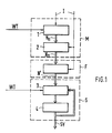
- a pulse I generated in the synchronous word detector for the synchronous word is fed twice to a measuring device M.
- the measuring device M contains a counter 1 and a register 2.
- This counter reading N n is transferred to register 2, which is controlled by the last pulse I.
- the filter F forms from the last received counter reading together with a fixed number of previously received counter readings a rounded to an integer N '.
- a signal generator S which consists of a down counter 3 and a comparator 4.
- the down counter 3 clocked by the word clock WT or by an integer multiple of the word clock WT, counts down from the mean value N' to zero.
- Each numerical value is fed to the comparator 4, which compares it with the numerical value zero.
- the comparator When zero is reached, the comparator generates a synchronizing signal SY from the numerical value, more precisely: the edge of a synchronizing signal SY, the clock period of the synchronizing signal SY being equal to the mean value N '.
- the synchronizing signal SY serves as a phase locked loop (PLL) as an input signal. It is returned to the down counter 3 so that it can record the next average N 'from the filter F.
- PLL phase locked loop
- FIG. 2 shows a first exemplary embodiment of the filter F from FIG. 1.
- a count N n becomes both an adder 21, where it is added to a sum of the register 2 shown in FIG. 1 from m summands of the last counter readings up to N n-1 as well as a shift register 22, in which the last m counter readings N nm to N n-1 are contained.
- the shift register 22 Whenever the shift register 22 is driven by a pulse I, the counter readings N i are shifted by one storage location, the new counter reading N n is set in the free storage location of the counter reading N n-1 , and the "oldest" counter reading N nm becomes given to a subtractor 23.
- This has two inputs, one of which is connected to the output of the shift register 22, the other to the output of the adder 21. It forms the difference from the sum from the output of the adder 21 and the count N nm of the shift register 22:
- the difference formed by the subtractor 23 is fed to a register 24, which is clocked again by the pulses I. From there it arrives on the one hand at a further adder 25, on the other hand back to the adder 21, in this way the new sum is formed.
- the sum of the difference and a rounding error R is formed in the adder 25.
- the sum is fed to a computing circuit 26 with two outputs, which forms the arithmetic mean of the counter readings N i and rounds the value obtained to an integer N ', forwards this to the signal generator S (see FIG. 1) and the rounding error R one Register 25 feeds, which, clocked by the pulses I, supplies the rounding error from the previous rounding to the adder 31 at the same time as the arrival of a new sum.
- the rounding errors R are used to maintain the clock repetition frequency on average.
- FIG. 3 Another embodiment of the filter F is shown in FIG. 3.
- the comparator 32 receives, via its other input, the counter reading from the output of a counter 33, which it compares with the value from the adder 31. If this is less than the counter reading of the counter 33, the comparator 32 lowers its counter reading by 1; conversely, if the value from the adder 31 is greater than the counter reading of the counter 33, it increases its counter reading. If both values are the same, it leaves it.
- the counter 33 is set to an assumed average counter reading via a line L before the circuit is started up, so that the filter F can work from the beginning.
- the counter 33 is clocked by the pulses I. Its output is connected to the input of the signal generator S shown in FIG. 1 and the subtractor 34.
- the subtractor 34 forms the difference between the counter reading of the counter 33 and the sum obtained from the adder 31.
- the difference formed by the subtractor 34 represents the error signal FS, which is fed to the register 35 clocked by the pulses I, which it supplies when the next counter reading N n + 1 arrives at the input of the adder 31.
- the adder 31 then again forms the sum of the counter reading N n + 1 and the error signal FS.
- the counter therefore passes on the output side much smaller fluctuations in the counter readings to the signal generator S than are present on the adder 31 on the input side.
Landscapes
- Engineering & Computer Science (AREA)
- Computer Networks & Wireless Communication (AREA)
- Signal Processing (AREA)
- Synchronisation In Digital Transmission Systems (AREA)
- Time-Division Multiplex Systems (AREA)
Applications Claiming Priority (2)
| Application Number | Priority Date | Filing Date | Title |
|---|---|---|---|
| DE3842694A DE3842694A1 (de) | 1988-12-19 | 1988-12-19 | Demultiplexer mit schaltung zur verringerung des wartezeitjitters |
| DE3842694 | 1988-12-19 |
Publications (3)
| Publication Number | Publication Date |
|---|---|
| EP0374537A2 true EP0374537A2 (fr) | 1990-06-27 |
| EP0374537A3 EP0374537A3 (fr) | 1991-10-09 |
| EP0374537B1 EP0374537B1 (fr) | 1995-04-26 |
Family
ID=6369516
Family Applications (1)
| Application Number | Title | Priority Date | Filing Date |
|---|---|---|---|
| EP89121962A Expired - Lifetime EP0374537B1 (fr) | 1988-12-19 | 1989-11-28 | Démultiplexeur avec circuit de réduction de la distorsion du temps d'attente |
Country Status (10)
| Country | Link |
|---|---|
| US (1) | US5062107A (fr) |
| EP (1) | EP0374537B1 (fr) |
| JP (1) | JP2510307B2 (fr) |
| KR (1) | KR970000066B1 (fr) |
| CN (1) | CN1014197B (fr) |
| AT (1) | ATE121886T1 (fr) |
| AU (1) | AU623458B2 (fr) |
| CA (1) | CA2005194C (fr) |
| DE (2) | DE3842694A1 (fr) |
| ES (1) | ES2074070T3 (fr) |
Cited By (1)
| Publication number | Priority date | Publication date | Assignee | Title |
|---|---|---|---|---|
| FR2737367A1 (fr) * | 1995-07-28 | 1997-01-31 | Thomson Multimedia Sa | Procede et dispositif de synchronisation d'horloges d'encodeurs et decodeurs numeriques |
Families Citing this family (4)
| Publication number | Priority date | Publication date | Assignee | Title |
|---|---|---|---|---|
| JPH0771060B2 (ja) * | 1990-04-10 | 1995-07-31 | シャープ株式会社 | フレーム同期保護回路 |
| IT1265424B1 (it) * | 1993-12-22 | 1996-11-22 | Alcatel Italia | Metodo e disposizione ciruitale di realizzazione della funzione di hpa negli apparati sdh |
| JP3203978B2 (ja) * | 1994-07-25 | 2001-09-04 | ソニー株式会社 | データ送受信装置、データ受信装置及びデータ送信装置 |
| US8094685B2 (en) * | 2006-10-04 | 2012-01-10 | Siemens Medical Solutions Usa, Inc. | Systems and methods for synchronizing multiple video streams |
Family Cites Families (11)
| Publication number | Priority date | Publication date | Assignee | Title |
|---|---|---|---|---|
| JPS4842917U (fr) * | 1971-09-25 | 1973-06-02 | ||
| GB1508986A (en) * | 1974-05-29 | 1978-04-26 | Post Office | Digital network synchronising system |
| US4144414A (en) * | 1978-01-23 | 1979-03-13 | Rockwell International Corporation | Network synchronization apparatus |
| JPS594900B2 (ja) * | 1979-09-03 | 1984-02-01 | 日本電気株式会社 | クロック再生回路 |
| FR2537363B1 (fr) * | 1982-12-02 | 1988-09-02 | Nippon Telegraph & Telephone | Dispositif de retablissement de signal d'horloge pour un systeme de telecommunication par satellite a acces multiple par repartition dans le temps |
| US4596024A (en) * | 1983-05-23 | 1986-06-17 | At&T Bell Laboratories | Data detector using probabalistic information in received signals |
| DE3439633A1 (de) * | 1984-10-30 | 1986-04-30 | Standard Elektrik Lorenz Ag, 7000 Stuttgart | Zeitmultiplex-uebertragungssystem, insbesondere fuer dienstintegrierte digitale breitbandnetze |
| US4718074A (en) * | 1986-03-25 | 1988-01-05 | Sotas, Inc. | Dejitterizer method and apparatus |
| US4746920A (en) * | 1986-03-28 | 1988-05-24 | Tandem Computers Incorporated | Method and apparatus for clock management |
| US4803726A (en) * | 1986-12-31 | 1989-02-07 | Motorola, Inc. | Bit synchronization method for a digital radio telephone system |
| BE1000415A7 (nl) * | 1987-03-18 | 1988-11-22 | Bell Telephone Mfg | Asynchroon op basis van tijdsverdeling werkend communicatiesysteem. |
-
1988
- 1988-12-19 DE DE3842694A patent/DE3842694A1/de not_active Withdrawn
-
1989
- 1989-11-28 EP EP89121962A patent/EP0374537B1/fr not_active Expired - Lifetime
- 1989-11-28 DE DE58909201T patent/DE58909201D1/de not_active Expired - Fee Related
- 1989-11-28 AT AT89121962T patent/ATE121886T1/de not_active IP Right Cessation
- 1989-11-28 ES ES89121962T patent/ES2074070T3/es not_active Expired - Lifetime
- 1989-12-12 CA CA002005194A patent/CA2005194C/fr not_active Expired - Fee Related
- 1989-12-13 AU AU46117/89A patent/AU623458B2/en not_active Ceased
- 1989-12-16 KR KR1019890018740A patent/KR970000066B1/ko not_active Expired - Fee Related
- 1989-12-18 US US07/452,212 patent/US5062107A/en not_active Expired - Lifetime
- 1989-12-19 JP JP1329373A patent/JP2510307B2/ja not_active Expired - Lifetime
- 1989-12-19 CN CN89109393A patent/CN1014197B/zh not_active Expired
Cited By (2)
| Publication number | Priority date | Publication date | Assignee | Title |
|---|---|---|---|---|
| FR2737367A1 (fr) * | 1995-07-28 | 1997-01-31 | Thomson Multimedia Sa | Procede et dispositif de synchronisation d'horloges d'encodeurs et decodeurs numeriques |
| EP0756394A3 (fr) * | 1995-07-28 | 1997-04-16 | Thomson Multimedia Sa | Procédé et dispositif de synchronisation d'horloges d'encodeurs et décodeurs numériques |
Also Published As
| Publication number | Publication date |
|---|---|
| KR970000066B1 (ko) | 1997-01-04 |
| CN1043840A (zh) | 1990-07-11 |
| DE58909201D1 (de) | 1995-06-01 |
| ATE121886T1 (de) | 1995-05-15 |
| EP0374537A3 (fr) | 1991-10-09 |
| JPH02217035A (ja) | 1990-08-29 |
| JP2510307B2 (ja) | 1996-06-26 |
| KR910013967A (ko) | 1991-08-08 |
| US5062107A (en) | 1991-10-29 |
| ES2074070T3 (es) | 1995-09-01 |
| AU4611789A (en) | 1990-06-21 |
| CN1014197B (zh) | 1991-10-02 |
| CA2005194A1 (fr) | 1990-06-19 |
| CA2005194C (fr) | 1994-08-16 |
| DE3842694A1 (de) | 1990-06-21 |
| AU623458B2 (en) | 1992-05-14 |
| EP0374537B1 (fr) | 1995-04-26 |
Similar Documents
| Publication | Publication Date | Title |
|---|---|---|
| DE3004799C2 (fr) | ||
| EP0141194A2 (fr) | Dispositif pour la synchronisation de trames et de phase d'une horloge d'échantillonnage du coté réception | |
| DE3111555C2 (de) | Verfahren und Vorrichtung zur Informationsspeicherung unter Anwendung früherer Aufzeichnung | |
| DE2437390B2 (de) | Verfahren zur Übertragung von binären Daten | |
| DE68921706T2 (de) | Synchrone Multiplexübertragungseinrichtung. | |
| EP0023331B1 (fr) | Circuit pour la synchronisation d'un dispositif subordonné, en particulier un poste d'abonné numérique par un dispositif d'ordre supérieur, en particulier un central de communication numérique d'un réseau de télécommunication MIC | |
| DE1226635B (de) | Verfahren und Schaltungsanordnung zur Fest-stellung fehlerhafter Impulsregenerierverstaerker | |
| DE3732287A1 (de) | Verfahren und schaltungsanordnung zum ableiten des worttaktes eines pulslagemodulierten signals | |
| EP0374537B1 (fr) | Démultiplexeur avec circuit de réduction de la distorsion du temps d'attente | |
| DE68909717T2 (de) | Verfahren zur Synchronisation und Anordnung zur Synchronisationsrückgewinnung für Übertragung in Zeitgetrenntlage. | |
| DE3881621T2 (de) | Jitterregelung in digitalen uebertragungsstrecken. | |
| DE68919437T2 (de) | Schaltungsanordnung zur Detektion von Kodeverletzungen in AMI-Signalübertragung. | |
| DE3246211C2 (de) | Schaltungsanordnung zur Detektion von Folgen identischer Binärwerte | |
| DE2613930B2 (de) | Digitaler Phasenregelkreis | |
| DE2933322A1 (de) | Schaltungsanordnung zum ableiten eines bittaktsignals aus einem digitalsignal | |
| DE3131406C2 (de) | Schaltung zur Synchronisation einer Sende/Empfangsstelle auf das Datennetz eines digitalen Nachrichtensystems | |
| EP0301481A1 (fr) | Dispositif de synchronisation pour un démultiplexeur de signaux numériques | |
| DE3590008T1 (de) | Gerät zur Synchronisierung von Impulsketten in einem digitalen Telefonsystem | |
| DE68927363T2 (de) | Datenübertragungssteuerungsschaltung | |
| DE2633031C3 (de) | Schaltungsanordnung zur Einstellung eines Binärzählers | |
| DE3202945C2 (de) | Verfahren und Anordnung zur Erzeugung von Fensterimpulsen (Daten- und gegebenenfalls Taktfensterimpulsen) für eine Separatorschaltung zur Trennung der Datenimpulse von Begleitimpulsen beim Lesen von Magnetband- oder Plattenspeichern, insbesondere von Floppy-Disk-Speichern | |
| DE2840952C2 (fr) | ||
| DE2350669C3 (de) | Verfahren zur Übertragung von Nachrichten mit wiederholter Übertragung gestörter Nachrichtenteile | |
| EP0508070B1 (fr) | Méthode et dispositif de reconnaissance de perte de synchronisation entre deux suites de mots d'un signal de référence et d'un signal de mesure | |
| EP0872974A2 (fr) | Dispositif de détection de motif d'erreur de bit |
Legal Events
| Date | Code | Title | Description |
|---|---|---|---|
| PUAI | Public reference made under article 153(3) epc to a published international application that has entered the european phase |
Free format text: ORIGINAL CODE: 0009012 |
|
| AK | Designated contracting states |
Kind code of ref document: A2 Designated state(s): AT BE CH DE ES FR GB IT LI NL SE |
|
| PUAL | Search report despatched |
Free format text: ORIGINAL CODE: 0009013 |
|
| AK | Designated contracting states |
Kind code of ref document: A3 Designated state(s): AT BE CH DE ES FR GB IT LI NL SE |
|
| 17P | Request for examination filed |
Effective date: 19911004 |
|
| 17Q | First examination report despatched |
Effective date: 19931018 |
|
| GRAA | (expected) grant |
Free format text: ORIGINAL CODE: 0009210 |
|
| AK | Designated contracting states |
Kind code of ref document: B1 Designated state(s): AT BE CH DE ES FR GB IT LI NL SE |
|
| REF | Corresponds to: |
Ref document number: 121886 Country of ref document: AT Date of ref document: 19950515 Kind code of ref document: T |
|
| REF | Corresponds to: |
Ref document number: 58909201 Country of ref document: DE Date of ref document: 19950601 |
|
| GBT | Gb: translation of ep patent filed (gb section 77(6)(a)/1977) |
Effective date: 19950515 |
|
| ITF | It: translation for a ep patent filed | ||
| ET | Fr: translation filed | ||
| REG | Reference to a national code |
Ref country code: ES Ref legal event code: FG2A Ref document number: 2074070 Country of ref document: ES Kind code of ref document: T3 |
|
| PLBE | No opposition filed within time limit |
Free format text: ORIGINAL CODE: 0009261 |
|
| STAA | Information on the status of an ep patent application or granted ep patent |
Free format text: STATUS: NO OPPOSITION FILED WITHIN TIME LIMIT |
|
| 26N | No opposition filed | ||
| PGFP | Annual fee paid to national office [announced via postgrant information from national office to epo] |
Ref country code: CH Payment date: 19991014 Year of fee payment: 11 Ref country code: NL Payment date: 19991014 Year of fee payment: 11 |
|
| PGFP | Annual fee paid to national office [announced via postgrant information from national office to epo] |
Ref country code: AT Payment date: 19991021 Year of fee payment: 11 |
|
| PGFP | Annual fee paid to national office [announced via postgrant information from national office to epo] |
Ref country code: BE Payment date: 19991122 Year of fee payment: 11 |
|
| PG25 | Lapsed in a contracting state [announced via postgrant information from national office to epo] |
Ref country code: AT Free format text: LAPSE BECAUSE OF NON-PAYMENT OF DUE FEES Effective date: 20001128 |
|
| PG25 | Lapsed in a contracting state [announced via postgrant information from national office to epo] |
Ref country code: LI Free format text: LAPSE BECAUSE OF NON-PAYMENT OF DUE FEES Effective date: 20001130 Ref country code: BE Free format text: LAPSE BECAUSE OF NON-PAYMENT OF DUE FEES Effective date: 20001130 Ref country code: CH Free format text: LAPSE BECAUSE OF NON-PAYMENT OF DUE FEES Effective date: 20001130 |
|
| BERE | Be: lapsed |
Owner name: ALCATEL N.V. Effective date: 20001130 |
|
| PG25 | Lapsed in a contracting state [announced via postgrant information from national office to epo] |
Ref country code: NL Free format text: LAPSE BECAUSE OF NON-PAYMENT OF DUE FEES Effective date: 20010601 |
|
| REG | Reference to a national code |
Ref country code: CH Ref legal event code: PL |
|
| NLV4 | Nl: lapsed or anulled due to non-payment of the annual fee |
Effective date: 20010601 |
|
| REG | Reference to a national code |
Ref country code: GB Ref legal event code: IF02 |
|
| PGFP | Annual fee paid to national office [announced via postgrant information from national office to epo] |
Ref country code: ES Payment date: 20071129 Year of fee payment: 19 Ref country code: DE Payment date: 20071123 Year of fee payment: 19 |
|
| PGFP | Annual fee paid to national office [announced via postgrant information from national office to epo] |
Ref country code: IT Payment date: 20071126 Year of fee payment: 19 |
|
| PGFP | Annual fee paid to national office [announced via postgrant information from national office to epo] |
Ref country code: SE Payment date: 20071114 Year of fee payment: 19 |
|
| PGFP | Annual fee paid to national office [announced via postgrant information from national office to epo] |
Ref country code: GB Payment date: 20071120 Year of fee payment: 19 Ref country code: FR Payment date: 20071122 Year of fee payment: 19 |
|
| EUG | Se: european patent has lapsed | ||
| GBPC | Gb: european patent ceased through non-payment of renewal fee |
Effective date: 20081128 |
|
| PG25 | Lapsed in a contracting state [announced via postgrant information from national office to epo] |
Ref country code: IT Free format text: LAPSE BECAUSE OF NON-PAYMENT OF DUE FEES Effective date: 20081128 |
|
| REG | Reference to a national code |
Ref country code: FR Ref legal event code: ST Effective date: 20090731 |
|
| PG25 | Lapsed in a contracting state [announced via postgrant information from national office to epo] |
Ref country code: DE Free format text: LAPSE BECAUSE OF NON-PAYMENT OF DUE FEES Effective date: 20090603 |
|
| PG25 | Lapsed in a contracting state [announced via postgrant information from national office to epo] |
Ref country code: GB Free format text: LAPSE BECAUSE OF NON-PAYMENT OF DUE FEES Effective date: 20081128 |
|
| REG | Reference to a national code |
Ref country code: ES Ref legal event code: FD2A Effective date: 20081129 |
|
| PG25 | Lapsed in a contracting state [announced via postgrant information from national office to epo] |
Ref country code: ES Free format text: LAPSE BECAUSE OF NON-PAYMENT OF DUE FEES Effective date: 20081129 |
|
| PG25 | Lapsed in a contracting state [announced via postgrant information from national office to epo] |
Ref country code: SE Free format text: LAPSE BECAUSE OF NON-PAYMENT OF DUE FEES Effective date: 20081129 |
|
| PG25 | Lapsed in a contracting state [announced via postgrant information from national office to epo] |
Ref country code: FR Free format text: LAPSE BECAUSE OF NON-PAYMENT OF DUE FEES Effective date: 20081130 |