EP0374537B1 - Démultiplexeur avec circuit de réduction de la distorsion du temps d'attente - Google Patents
Démultiplexeur avec circuit de réduction de la distorsion du temps d'attente Download PDFInfo
- Publication number
- EP0374537B1 EP0374537B1 EP89121962A EP89121962A EP0374537B1 EP 0374537 B1 EP0374537 B1 EP 0374537B1 EP 89121962 A EP89121962 A EP 89121962A EP 89121962 A EP89121962 A EP 89121962A EP 0374537 B1 EP0374537 B1 EP 0374537B1
- Authority
- EP
- European Patent Office
- Prior art keywords
- sync
- signal
- sync words
- counter
- demultiplexer
- Prior art date
- Legal status (The legal status is an assumption and is not a legal conclusion. Google has not performed a legal analysis and makes no representation as to the accuracy of the status listed.)
- Expired - Lifetime
Links
- 238000012935 Averaging Methods 0.000 claims 1
- 230000001360 synchronised effect Effects 0.000 description 9
- 230000005540 biological transmission Effects 0.000 description 5
- 238000000034 method Methods 0.000 description 2
- 230000003044 adaptive effect Effects 0.000 description 1
- 238000010586 diagram Methods 0.000 description 1
- 238000003780 insertion Methods 0.000 description 1
- 230000037431 insertion Effects 0.000 description 1
- 230000003068 static effect Effects 0.000 description 1
- 230000002123 temporal effect Effects 0.000 description 1
Images


Classifications
-
- H—ELECTRICITY
- H04—ELECTRIC COMMUNICATION TECHNIQUE
- H04Q—SELECTING
- H04Q11/00—Selecting arrangements for multiplex systems
- H04Q11/04—Selecting arrangements for multiplex systems for time-division multiplexing
-
- H—ELECTRICITY
- H04—ELECTRIC COMMUNICATION TECHNIQUE
- H04J—MULTIPLEX COMMUNICATION
- H04J3/00—Time-division multiplex systems
- H04J3/02—Details
- H04J3/06—Synchronising arrangements
- H04J3/0602—Systems characterised by the synchronising information used
-
- H—ELECTRICITY
- H04—ELECTRIC COMMUNICATION TECHNIQUE
- H04J—MULTIPLEX COMMUNICATION
- H04J3/00—Time-division multiplex systems
- H04J3/02—Details
- H04J3/06—Synchronising arrangements
- H04J3/07—Synchronising arrangements using pulse stuffing for systems with different or fluctuating information rates or bit rates
Definitions
- the invention relates to a demultiplexer according to the preamble of patent claim 1.
- Such a demultiplexer is known from DE-A1-34 39 633.
- the synchronous signal is derived from the word clock of the received sequence of synchronous words in that the word clock is corrected with the aid of additional information transmitted to the demultiplexer such that the spacing between its successive clock pulses are equal to the intervals of the synchronous words of the digital signal to be inserted into the pulse frame by the multiplexer at the transmission end and asynchronous to the pulse frame.
- the clock fluctuation of the synchronous words caused by the insertion of this signal asynchronously to the pulse frame, the so-called "waiting time jitter" is thus significantly reduced in the demultiplexer.
- a disadvantage of this solution is that a circuit for generating the additional information is necessary on the transmission side and that transmission capacity is lost as a result of its transmission.
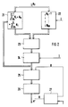
- a pulse I generated in the synchronous word detector for the synchronous word is fed twice to a measuring device M.
- the measuring device M contains a counter 1 and a register 2.
- Kalman filter for reporting the estimated clock frequency error ⁇ f (K) is described.
- the above article describes complex static methods for determining the desired clock frequency f2 (K).
- a device with means for demultiplexing a data signal asynchronous to a pulse frame and disturbed by a waiting time jitter is not described.
- This counter reading N n is transferred to register 2, which is controlled by the last pulse I.
- the filter F forms from the last received counter reading together with a fixed number of previously received counter readings a rounded to an integer N '.
- a signal generator S which consists of a down counter 3 and a comparator 4.
- the down counter 3 clocked by the word clock WT or by an integer multiple of the word clock WT, counts down to zero from the mean value N'.
- Each numerical value is fed to the comparator 4, which compares it with the numerical value zero.
- the comparator When zero is reached, the comparator generates a synchronizing signal SY from the numerical value, more precisely: the edge of a synchronizing signal SY, the clock period of the synchronizing signal SY being equal to the mean value N '.
- the synchronizing signal SY serves as a phase locked loop (PLL) as an input signal. It is returned to the down counter 3 so that it can record the next mean N 'from the filter F.
- PLL phase locked loop
- FIG. 2 shows a first exemplary embodiment of the filter F from FIG. 1.
- a counter reading N n becomes both an adder 21, where it is added to a sum of the register 2 shown in FIG. 1 from m summands of the last counter readings up to N n-1 as well as a shift register 22, in which the last m counter readings N nm to N n-1 are contained.
- the shift register 22 Whenever the shift register 22 is driven by a pulse I, the counter readings N i are shifted by one storage location, the new counter reading N n is set in the free storage location of the counter reading N n-1 , and the "oldest" counter reading N nm becomes given to a subtractor 23.
- This has two inputs, one of which is connected to the output of the shift register 22, the other to the output of the adder 21. It forms the difference from the sum from the output of the adder 21 and the count N nm of the shift register 22:
- the difference formed by the subtractor 23 is fed to a register 24, which is clocked again by the pulses I. From there it arrives on the one hand at a further adder 25, on the other hand back to the adder 21, in this way the new sum is formed.
- the sum of the difference and a rounding error R is formed in the adder 25.
- the sum is fed to a computing circuit 26 with two outputs, which forms the arithmetic mean of the counter readings N i and rounds the value obtained to an integer N ', forwards this to the signal generator S (see FIG. 1) and the rounding error R one Register 25 feeds, which, clocked by the pulses I, supplies the rounding error from the previous rounding to the adder 31 at the same time as the arrival of a new sum.
- the rounding errors R are used to maintain the clock repetition frequency on average.
- FIG. 3 Another embodiment of the filter F is shown in FIG. 3.
- the comparator 32 receives, via its other input, the counter reading from the output of a counter 33, which it compares with the value from the adder 31. If this is less than the counter reading of the counter 33, the comparator 32 lowers its counter reading by 1; conversely, if the value from the adder 31 is greater than the counter reading of the counter 33, it increases its counter reading. If both values are the same, it leaves it.
- the counter 33 is set to an assumed average counter reading via a line L before the circuit is started up, so that the filter F can work from the beginning.
- the counter 33 is clocked by the pulses I. Its output is connected to the input of the signal generator S shown in FIG. 1 and the subtractor 34.
- the subtractor 34 forms the difference between the counter reading of the counter 33 and the sum obtained from the adder 31.
- the difference formed by the subtractor 34 represents the error signal FS, which is fed to the register 35 clocked by the pulses I, which it supplies to the adder 31 when the next counter reading N n + 1 arrives.
- the adder 31 then again forms the sum of the counter reading N n + 1 and the error signal FS.
- the counter therefore passes on the output side much smaller fluctuations in the counter readings to the signal generator S than are present on the adder 31 on the input side.
Landscapes
- Engineering & Computer Science (AREA)
- Computer Networks & Wireless Communication (AREA)
- Signal Processing (AREA)
- Synchronisation In Digital Transmission Systems (AREA)
- Time-Division Multiplex Systems (AREA)
Claims (3)
- Démultiplexeur pour un système numérique de transmission de l'information en multiplexage par répartition dans le temps, dans le cas duquel on insère dans le train d'impulsions un signal numérique qui est asynchrone par rapport au train d'impulsions, qui est constitué de blocs successifs et dont les débuts de bloc sont chacun repérés par un mot de synchronisation, comportant un circuit qui, à partir du rythme de la suite, reçue, des mots de synchronisation, dérive un signal de synchronisation (SY) qui présente une fluctuation de rythme plus faible que celle du rythme de la suite, reçue, des mots de synchronisation,
caractérisé
par le fait qu'il contient: un dispositif de mesure (M) qui mesure les intervalles de temps (N) entre les mots de synchronisation reçus, un filtre (F) qui, à partir des intervalles de temps (N) des mots de synchronisation, forme une valeur moyenne (N′), et un producteur de signaux (S) qui, à partir de la valeur moyenne (N′), forme un signal de synchronisation (SY) de façon telle que sa période de rythme est égale à la valeur moyenne (N′). - Démultiplexeur selon la revendication 1,
caractérisé
par le fait que le filtre (F) forme la moyenne arithmétique (N′) des intervalles de temps pour les différents intervalles de temps (Ni), différents et successivement mesurés au cours d'une période de temps prescrite, des mots de synchronisation successifs, et arrondit cette valeur moyenne à un nombre entier N′, l'erreur d'arrondi (R), qui résulte de l'arrondi lors de la formation de la valeur moyenne, étant prise en compte, au moyen d'une rétroaction d'erreur, pour la formation de la valeur moyenne qui suit. - Démultiplexeur selon la revendication 1,
caractérisé
par le fait que le filtre (F) contient un compteur (33) dans lequel, avant mise en service du circuit, on mémorise un intervalle de temps moyen, admis, des mots de synchronisation, par le fait que le compteur (33) ne peut qu'élever ou abaisser, d'une valeur fixe, une fois pendant un intervalle de temps entre deux mots de synchronisation, I'état de comptage (N′) qui y est justement contenu, ou bien le laisser inchangé, et par le fait que cette modification est déterminée à partir du résultat d'une comparaison d'états de comptage entre d'une part l'état de comptage (N′) mémorisé dans le compteur (33) et d'autre part la somme d'un état de comptage suivant (Nn+1) à l'entrée du filtre (F) et d'un signal d'erreur (FS).
Applications Claiming Priority (2)
| Application Number | Priority Date | Filing Date | Title |
|---|---|---|---|
| DE3842694 | 1988-12-19 | ||
| DE3842694A DE3842694A1 (de) | 1988-12-19 | 1988-12-19 | Demultiplexer mit schaltung zur verringerung des wartezeitjitters |
Publications (3)
| Publication Number | Publication Date |
|---|---|
| EP0374537A2 EP0374537A2 (fr) | 1990-06-27 |
| EP0374537A3 EP0374537A3 (fr) | 1991-10-09 |
| EP0374537B1 true EP0374537B1 (fr) | 1995-04-26 |
Family
ID=6369516
Family Applications (1)
| Application Number | Title | Priority Date | Filing Date |
|---|---|---|---|
| EP89121962A Expired - Lifetime EP0374537B1 (fr) | 1988-12-19 | 1989-11-28 | Démultiplexeur avec circuit de réduction de la distorsion du temps d'attente |
Country Status (10)
| Country | Link |
|---|---|
| US (1) | US5062107A (fr) |
| EP (1) | EP0374537B1 (fr) |
| JP (1) | JP2510307B2 (fr) |
| KR (1) | KR970000066B1 (fr) |
| CN (1) | CN1014197B (fr) |
| AT (1) | ATE121886T1 (fr) |
| AU (1) | AU623458B2 (fr) |
| CA (1) | CA2005194C (fr) |
| DE (2) | DE3842694A1 (fr) |
| ES (1) | ES2074070T3 (fr) |
Families Citing this family (5)
| Publication number | Priority date | Publication date | Assignee | Title |
|---|---|---|---|---|
| JPH0771060B2 (ja) * | 1990-04-10 | 1995-07-31 | シャープ株式会社 | フレーム同期保護回路 |
| IT1265424B1 (it) * | 1993-12-22 | 1996-11-22 | Alcatel Italia | Metodo e disposizione ciruitale di realizzazione della funzione di hpa negli apparati sdh |
| JP3203978B2 (ja) * | 1994-07-25 | 2001-09-04 | ソニー株式会社 | データ送受信装置、データ受信装置及びデータ送信装置 |
| FR2737367B1 (fr) * | 1995-07-28 | 1997-10-17 | Thomson Multimedia Sa | Procede et dispositif de synchronisation d'horloges d'encodeurs et decodeurs numeriques |
| US8094685B2 (en) * | 2006-10-04 | 2012-01-10 | Siemens Medical Solutions Usa, Inc. | Systems and methods for synchronizing multiple video streams |
Family Cites Families (11)
| Publication number | Priority date | Publication date | Assignee | Title |
|---|---|---|---|---|
| JPS4842917U (fr) * | 1971-09-25 | 1973-06-02 | ||
| GB1508986A (en) * | 1974-05-29 | 1978-04-26 | Post Office | Digital network synchronising system |
| US4144414A (en) * | 1978-01-23 | 1979-03-13 | Rockwell International Corporation | Network synchronization apparatus |
| JPS594900B2 (ja) * | 1979-09-03 | 1984-02-01 | 日本電気株式会社 | クロック再生回路 |
| FR2537363B1 (fr) * | 1982-12-02 | 1988-09-02 | Nippon Telegraph & Telephone | Dispositif de retablissement de signal d'horloge pour un systeme de telecommunication par satellite a acces multiple par repartition dans le temps |
| US4596024A (en) * | 1983-05-23 | 1986-06-17 | At&T Bell Laboratories | Data detector using probabalistic information in received signals |
| DE3439633A1 (de) * | 1984-10-30 | 1986-04-30 | Standard Elektrik Lorenz Ag, 7000 Stuttgart | Zeitmultiplex-uebertragungssystem, insbesondere fuer dienstintegrierte digitale breitbandnetze |
| US4718074A (en) * | 1986-03-25 | 1988-01-05 | Sotas, Inc. | Dejitterizer method and apparatus |
| US4746920A (en) * | 1986-03-28 | 1988-05-24 | Tandem Computers Incorporated | Method and apparatus for clock management |
| US4803726A (en) * | 1986-12-31 | 1989-02-07 | Motorola, Inc. | Bit synchronization method for a digital radio telephone system |
| BE1000415A7 (nl) * | 1987-03-18 | 1988-11-22 | Bell Telephone Mfg | Asynchroon op basis van tijdsverdeling werkend communicatiesysteem. |
-
1988
- 1988-12-19 DE DE3842694A patent/DE3842694A1/de not_active Withdrawn
-
1989
- 1989-11-28 AT AT89121962T patent/ATE121886T1/de not_active IP Right Cessation
- 1989-11-28 DE DE58909201T patent/DE58909201D1/de not_active Expired - Fee Related
- 1989-11-28 EP EP89121962A patent/EP0374537B1/fr not_active Expired - Lifetime
- 1989-11-28 ES ES89121962T patent/ES2074070T3/es not_active Expired - Lifetime
- 1989-12-12 CA CA002005194A patent/CA2005194C/fr not_active Expired - Fee Related
- 1989-12-13 AU AU46117/89A patent/AU623458B2/en not_active Ceased
- 1989-12-16 KR KR1019890018740A patent/KR970000066B1/ko not_active Expired - Fee Related
- 1989-12-18 US US07/452,212 patent/US5062107A/en not_active Expired - Lifetime
- 1989-12-19 CN CN89109393A patent/CN1014197B/zh not_active Expired
- 1989-12-19 JP JP1329373A patent/JP2510307B2/ja not_active Expired - Lifetime
Also Published As
| Publication number | Publication date |
|---|---|
| JPH02217035A (ja) | 1990-08-29 |
| AU623458B2 (en) | 1992-05-14 |
| CA2005194A1 (fr) | 1990-06-19 |
| DE3842694A1 (de) | 1990-06-21 |
| EP0374537A2 (fr) | 1990-06-27 |
| EP0374537A3 (fr) | 1991-10-09 |
| CA2005194C (fr) | 1994-08-16 |
| ES2074070T3 (es) | 1995-09-01 |
| CN1043840A (zh) | 1990-07-11 |
| AU4611789A (en) | 1990-06-21 |
| DE58909201D1 (de) | 1995-06-01 |
| KR910013967A (ko) | 1991-08-08 |
| KR970000066B1 (ko) | 1997-01-04 |
| CN1014197B (zh) | 1991-10-02 |
| ATE121886T1 (de) | 1995-05-15 |
| JP2510307B2 (ja) | 1996-06-26 |
| US5062107A (en) | 1991-10-29 |
Similar Documents
| Publication | Publication Date | Title |
|---|---|---|
| DE69132924T2 (de) | Anordnung für synchrone Informationsübertragung über ein asynchrones Netzwerk, insbesondere über ein ATM-Netzwerk | |
| DE4017494C2 (fr) | ||
| DE3875484T2 (de) | Asynchrones zeitmultiplex-kommunikationssystem. | |
| DE69621725T2 (de) | System zur bereitstellung eines vorgegebenen zeitbezugs zwischen eingabe und ausgabe von daten sowie sender und empfänger für ein solches system | |
| EP0507385B1 (fr) | Système de transmission pour la hiérarchie numérique synchrone | |
| DE3687133T2 (de) | Schaltung und verfahren zur geschwindigkeitsanpassung fuer asynchrone daten in digitalen netzwerken. | |
| EP0141194A2 (fr) | Dispositif pour la synchronisation de trames et de phase d'une horloge d'échantillonnage du coté réception | |
| DE69115563T2 (de) | Verfahren zum Vermindern von Niederfrequenz-Zitterkomponenten in einem digitalen Daten-Übertragungssystem | |
| EP0475498A2 (fr) | Circuit d'adaption du débit binaire de deux signaux numériques | |
| EP0356548A1 (fr) | Procédé et circuit pour contrôler numériquement la fréquence et/ou la phase des impulsions d'une horloge d'échantillonnage | |
| DE68921706T2 (de) | Synchrone Multiplexübertragungseinrichtung. | |
| DE1226635B (de) | Verfahren und Schaltungsanordnung zur Fest-stellung fehlerhafter Impulsregenerierverstaerker | |
| EP0374537B1 (fr) | Démultiplexeur avec circuit de réduction de la distorsion du temps d'attente | |
| DE3881621T2 (de) | Jitterregelung in digitalen uebertragungsstrecken. | |
| DE68909717T2 (de) | Verfahren zur Synchronisation und Anordnung zur Synchronisationsrückgewinnung für Übertragung in Zeitgetrenntlage. | |
| DE3888133T2 (de) | Datenmustersynchronisiereinrichtung. | |
| DE3435097C2 (fr) | ||
| DE2855082A1 (de) | Uebertragungssystem fuer digitale signale | |
| EP0301481B1 (fr) | Dispositif de synchronisation pour un démultiplexeur de signaux numériques | |
| DE4132325C2 (de) | Anordnung zum automatischen Taktabgleich bei integrierten Schaltkreisen | |
| DE3131406C2 (de) | Schaltung zur Synchronisation einer Sende/Empfangsstelle auf das Datennetz eines digitalen Nachrichtensystems | |
| DE2933322A1 (de) | Schaltungsanordnung zum ableiten eines bittaktsignals aus einem digitalsignal | |
| DE4111176C1 (fr) | ||
| DE69425029T2 (de) | Anordnung zur Filterung des Phasenzitterns wegen Entfernen positiver Stopfbits und Anwendung zur Filterung des Phasenzitterns wegen Entfernen positiver und negativer Stopfbits einer digitalen Impulsfolge | |
| DE68905630T2 (de) | Verfahren und anordnung zur synchronisation von terminals, die ueber eine kette ohne zeittransparenz kommunizieren. |
Legal Events
| Date | Code | Title | Description |
|---|---|---|---|
| PUAI | Public reference made under article 153(3) epc to a published international application that has entered the european phase |
Free format text: ORIGINAL CODE: 0009012 |
|
| AK | Designated contracting states |
Kind code of ref document: A2 Designated state(s): AT BE CH DE ES FR GB IT LI NL SE |
|
| PUAL | Search report despatched |
Free format text: ORIGINAL CODE: 0009013 |
|
| AK | Designated contracting states |
Kind code of ref document: A3 Designated state(s): AT BE CH DE ES FR GB IT LI NL SE |
|
| 17P | Request for examination filed |
Effective date: 19911004 |
|
| 17Q | First examination report despatched |
Effective date: 19931018 |
|
| GRAA | (expected) grant |
Free format text: ORIGINAL CODE: 0009210 |
|
| AK | Designated contracting states |
Kind code of ref document: B1 Designated state(s): AT BE CH DE ES FR GB IT LI NL SE |
|
| REF | Corresponds to: |
Ref document number: 121886 Country of ref document: AT Date of ref document: 19950515 Kind code of ref document: T |
|
| REF | Corresponds to: |
Ref document number: 58909201 Country of ref document: DE Date of ref document: 19950601 |
|
| GBT | Gb: translation of ep patent filed (gb section 77(6)(a)/1977) |
Effective date: 19950515 |
|
| ITF | It: translation for a ep patent filed | ||
| ET | Fr: translation filed | ||
| REG | Reference to a national code |
Ref country code: ES Ref legal event code: FG2A Ref document number: 2074070 Country of ref document: ES Kind code of ref document: T3 |
|
| PLBE | No opposition filed within time limit |
Free format text: ORIGINAL CODE: 0009261 |
|
| STAA | Information on the status of an ep patent application or granted ep patent |
Free format text: STATUS: NO OPPOSITION FILED WITHIN TIME LIMIT |
|
| 26N | No opposition filed | ||
| PGFP | Annual fee paid to national office [announced via postgrant information from national office to epo] |
Ref country code: CH Payment date: 19991014 Year of fee payment: 11 Ref country code: NL Payment date: 19991014 Year of fee payment: 11 |
|
| PGFP | Annual fee paid to national office [announced via postgrant information from national office to epo] |
Ref country code: AT Payment date: 19991021 Year of fee payment: 11 |
|
| PGFP | Annual fee paid to national office [announced via postgrant information from national office to epo] |
Ref country code: BE Payment date: 19991122 Year of fee payment: 11 |
|
| PG25 | Lapsed in a contracting state [announced via postgrant information from national office to epo] |
Ref country code: AT Free format text: LAPSE BECAUSE OF NON-PAYMENT OF DUE FEES Effective date: 20001128 |
|
| PG25 | Lapsed in a contracting state [announced via postgrant information from national office to epo] |
Ref country code: LI Free format text: LAPSE BECAUSE OF NON-PAYMENT OF DUE FEES Effective date: 20001130 Ref country code: BE Free format text: LAPSE BECAUSE OF NON-PAYMENT OF DUE FEES Effective date: 20001130 Ref country code: CH Free format text: LAPSE BECAUSE OF NON-PAYMENT OF DUE FEES Effective date: 20001130 |
|
| BERE | Be: lapsed |
Owner name: ALCATEL N.V. Effective date: 20001130 |
|
| PG25 | Lapsed in a contracting state [announced via postgrant information from national office to epo] |
Ref country code: NL Free format text: LAPSE BECAUSE OF NON-PAYMENT OF DUE FEES Effective date: 20010601 |
|
| REG | Reference to a national code |
Ref country code: CH Ref legal event code: PL |
|
| NLV4 | Nl: lapsed or anulled due to non-payment of the annual fee |
Effective date: 20010601 |
|
| REG | Reference to a national code |
Ref country code: GB Ref legal event code: IF02 |
|
| PGFP | Annual fee paid to national office [announced via postgrant information from national office to epo] |
Ref country code: ES Payment date: 20071129 Year of fee payment: 19 Ref country code: DE Payment date: 20071123 Year of fee payment: 19 |
|
| PGFP | Annual fee paid to national office [announced via postgrant information from national office to epo] |
Ref country code: IT Payment date: 20071126 Year of fee payment: 19 |
|
| PGFP | Annual fee paid to national office [announced via postgrant information from national office to epo] |
Ref country code: SE Payment date: 20071114 Year of fee payment: 19 |
|
| PGFP | Annual fee paid to national office [announced via postgrant information from national office to epo] |
Ref country code: GB Payment date: 20071120 Year of fee payment: 19 Ref country code: FR Payment date: 20071122 Year of fee payment: 19 |
|
| EUG | Se: european patent has lapsed | ||
| GBPC | Gb: european patent ceased through non-payment of renewal fee |
Effective date: 20081128 |
|
| PG25 | Lapsed in a contracting state [announced via postgrant information from national office to epo] |
Ref country code: IT Free format text: LAPSE BECAUSE OF NON-PAYMENT OF DUE FEES Effective date: 20081128 |
|
| REG | Reference to a national code |
Ref country code: FR Ref legal event code: ST Effective date: 20090731 |
|
| PG25 | Lapsed in a contracting state [announced via postgrant information from national office to epo] |
Ref country code: DE Free format text: LAPSE BECAUSE OF NON-PAYMENT OF DUE FEES Effective date: 20090603 |
|
| PG25 | Lapsed in a contracting state [announced via postgrant information from national office to epo] |
Ref country code: GB Free format text: LAPSE BECAUSE OF NON-PAYMENT OF DUE FEES Effective date: 20081128 |
|
| REG | Reference to a national code |
Ref country code: ES Ref legal event code: FD2A Effective date: 20081129 |
|
| PG25 | Lapsed in a contracting state [announced via postgrant information from national office to epo] |
Ref country code: ES Free format text: LAPSE BECAUSE OF NON-PAYMENT OF DUE FEES Effective date: 20081129 |
|
| PG25 | Lapsed in a contracting state [announced via postgrant information from national office to epo] |
Ref country code: SE Free format text: LAPSE BECAUSE OF NON-PAYMENT OF DUE FEES Effective date: 20081129 |
|
| PG25 | Lapsed in a contracting state [announced via postgrant information from national office to epo] |
Ref country code: FR Free format text: LAPSE BECAUSE OF NON-PAYMENT OF DUE FEES Effective date: 20081130 |