EP0375231A2 - Silicium-Trägerstruktur für optische Halbleitervorrichtungen - Google Patents
Silicium-Trägerstruktur für optische Halbleitervorrichtungen Download PDFInfo
- Publication number
- EP0375231A2 EP0375231A2 EP89312877A EP89312877A EP0375231A2 EP 0375231 A2 EP0375231 A2 EP 0375231A2 EP 89312877 A EP89312877 A EP 89312877A EP 89312877 A EP89312877 A EP 89312877A EP 0375231 A2 EP0375231 A2 EP 0375231A2
- Authority
- EP
- European Patent Office
- Prior art keywords
- substrate
- stripline
- optical device
- silicon
- semiconductor optical
- Prior art date
- Legal status (The legal status is an assumption and is not a legal conclusion. Google has not performed a legal analysis and makes no representation as to the accuracy of the status listed.)
- Granted
Links
Images

Classifications
-
- H—ELECTRICITY
- H01—ELECTRIC ELEMENTS
- H01S—DEVICES USING THE PROCESS OF LIGHT AMPLIFICATION BY STIMULATED EMISSION OF RADIATION [LASER] TO AMPLIFY OR GENERATE LIGHT; DEVICES USING STIMULATED EMISSION OF ELECTROMAGNETIC RADIATION IN WAVE RANGES OTHER THAN OPTICAL
- H01S5/00—Semiconductor lasers
- H01S5/02—Structural details or components not essential to laser action
- H01S5/022—Mountings; Housings
- H01S5/0233—Mounting configuration of laser chips
- H01S5/02345—Wire-bonding
-
- H—ELECTRICITY
- H01—ELECTRIC ELEMENTS
- H01S—DEVICES USING THE PROCESS OF LIGHT AMPLIFICATION BY STIMULATED EMISSION OF RADIATION [LASER] TO AMPLIFY OR GENERATE LIGHT; DEVICES USING STIMULATED EMISSION OF ELECTROMAGNETIC RADIATION IN WAVE RANGES OTHER THAN OPTICAL
- H01S5/00—Semiconductor lasers
- H01S5/04—Processes or apparatus for excitation, e.g. pumping, e.g. by electron beams
- H01S5/042—Electrical excitation ; Circuits therefor
- H01S5/0427—Electrical excitation ; Circuits therefor for applying modulation to the laser
-
- H—ELECTRICITY
- H01—ELECTRIC ELEMENTS
- H01S—DEVICES USING THE PROCESS OF LIGHT AMPLIFICATION BY STIMULATED EMISSION OF RADIATION [LASER] TO AMPLIFY OR GENERATE LIGHT; DEVICES USING STIMULATED EMISSION OF ELECTROMAGNETIC RADIATION IN WAVE RANGES OTHER THAN OPTICAL
- H01S5/00—Semiconductor lasers
- H01S5/06—Arrangements for controlling the laser output parameters, e.g. by operating on the active medium
- H01S5/062—Arrangements for controlling the laser output parameters, e.g. by operating on the active medium by varying the potential of the electrodes
- H01S5/06226—Modulation at ultra-high frequencies
-
- H—ELECTRICITY
- H10—SEMICONDUCTOR DEVICES; ELECTRIC SOLID-STATE DEVICES NOT OTHERWISE PROVIDED FOR
- H10W—GENERIC PACKAGES, INTERCONNECTIONS, CONNECTORS OR OTHER CONSTRUCTIONAL DETAILS OF DEVICES COVERED BY CLASS H10
- H10W72/00—Interconnections or connectors in packages
- H10W72/50—Bond wires
- H10W72/531—Shapes of wire connectors
- H10W72/533—Cross-sectional shape
- H10W72/534—Cross-sectional shape being rectangular
-
- H—ELECTRICITY
- H10—SEMICONDUCTOR DEVICES; ELECTRIC SOLID-STATE DEVICES NOT OTHERWISE PROVIDED FOR
- H10W—GENERIC PACKAGES, INTERCONNECTIONS, CONNECTORS OR OTHER CONSTRUCTIONAL DETAILS OF DEVICES COVERED BY CLASS H10
- H10W72/00—Interconnections or connectors in packages
- H10W72/50—Bond wires
- H10W72/531—Shapes of wire connectors
- H10W72/536—Shapes of wire connectors the connected ends being ball-shaped
-
- Y—GENERAL TAGGING OF NEW TECHNOLOGICAL DEVELOPMENTS; GENERAL TAGGING OF CROSS-SECTIONAL TECHNOLOGIES SPANNING OVER SEVERAL SECTIONS OF THE IPC; TECHNICAL SUBJECTS COVERED BY FORMER USPC CROSS-REFERENCE ART COLLECTIONS [XRACs] AND DIGESTS
- Y10—TECHNICAL SUBJECTS COVERED BY FORMER USPC
- Y10S—TECHNICAL SUBJECTS COVERED BY FORMER USPC CROSS-REFERENCE ART COLLECTIONS [XRACs] AND DIGESTS
- Y10S257/00—Active solid-state devices, e.g. transistors, solid-state diodes
- Y10S257/903—FET configuration adapted for use as static memory cell
- Y10S257/904—FET configuration adapted for use as static memory cell with passive components,, e.g. polysilicon resistors
Definitions
- the present invention relates to a semiconductor optical device mounting structure and, more particularly, to a silicon-based stripline structure for providing an interconnection between the semiconductor optical device and a high frequency modulation current source.
- Semiconductor optical devices such as lasers and light emitting diodes (LEDs) are used in a wide variety of applications, due to their compactness, relatively high efficiency, and well-controlled output.
- LEDs light emitting diodes
- a number of requirements are imposed upon these devices.
- cooling of the optical device is necessary, since prolonged high temperature operation can seriously damage and even destroy the device.
- the output light intensity from the device is a function of its junction temperature, the supporting structure must be able to dissipate the tremendous amount of heat generated by the high current density in the device in its operating state.
- thermo-electric cooler While it is relatively simple to solve these temperature related problems (by use of a thermo-electric cooler, for example), other problems develop when a semiconductor optical device is operated at extremely high bit rates, for example, above 1 Gb/s. At these speeds, the low impedance of the laser relative to that of the modulation current source, as well as the parasitics associated with the interconnecting network, become critical factors. Minimizing these parasitics by matching the network impedance to the optical device impedance over a broad bandwidth must be performed in order to achieve acceptable performance. It is well-known that semiconductor devices such as lasers exhibit an impedance in the range of 2-8 ⁇ , while most high frequency modulation current sources have a relatively high output impedance (»50 ⁇ , typically).
- a problem with this approach is that since every laser exhibits a slightly different impedance (related to processing variations), each stripline of the Selway et al. design would have to be individually designed to match the particular laser to which it is being coupled. Further, in trying to use the stripline to directly match the impedance of the laser to the modulation current source, other problems develop. In general, to provide impedance matching, the ideal solution is either to decrease the impedance looking back from the laser to the source (so that the source appears to the laser as an equivalent load) or, alternatively, to increase the resistance of the laser as seen by the supply. For many reasons, however, these alternatives are impractical, if not impossible.
- the present invention relates to a mounting structure for semiconductor optical devices and, more particularly, to a silicon-based stripline structure for providing an interconnection with improved impedance matching between the optical device and a high frequency modulation current source.
- It is an aspect of the present invention to provide a stripline interconnection with reduced parasitic elements comprising a silicon substrate as the dielectric, with the top and bottom surfaces of the silicon metallized to form the signal and ground conductors of the stripline.
- the thickness of the silicon substrate and the width of the signal conductor are chosen to provide a stripline having the desired characteristic impedance, as will be described in detail below.
- the value of the deposited thin film resistor may be individually tailored such that matching will be provided, regardless of the laser's specific resistance. By forming the resistor adjacent to the laser, the value of the parasitic inductor associated with the spacing between these two elements will be significantly reduced.
- An advantage of the present invention is that the interconnection is silicon-based, allowing well-known silicon processing techniques to be used in the formation of the laser/modulation source interconnection.
- a metallized via is formed through the silicon substrate to facilitate the interconnection of the bottom conductor of the stripline to the top side of the laser chip.
- the use of the via technique has been found to significantly shorten this interconnection (otherwise formed by means of a number of wirebonds).
- the length of these wirebond interconnections increases the parasitic inductance of the interconnection and therefore becomes a serious concern at high bit rates. Shortening these interconnection paths in accordance with the invention decreases the parasitic elements mentioned above, thus providing improved performance of the mounted laser, in terms of bandwidth.
- the silicon fabrication techniques allow for the impedance matching resistor to be formed adjacent to the laser. This close placement thus reduces parasitics by reducing the spacing between the resistor and the laser.
- the silicon-based stripline mounts may be produced in mass quantities, with thousands being included on a single wafer. This volume represents orders of magnitude increase in fabrication efficiency over previous arrangements which used ceramics or other materials and required individual fabrication. The commensurate savings in expense is obvious.
- a silicon-based stripline mount 10 of the present invention for providing an interconnection between a semiconductor optical device and a high frequency modulation current source is illustrated in FIG. 1.
- an exemplary semiconductor optical device such as a laser 12 and impedance matching resistor 14 are located on the top surface 17 of a silicon substrate 16.
- a similar mount formed in accordance with the present invention may be utilized with other semiconductor optical devices, such as edge-emitting LEDs.
- the thickness t of substrate 16 is chosen to provide the desired characteristic impedance Z S of the transmission line.
- First and second conductors 18 and 24 provide, in conjunction with substrate 16, a first transmission line section A from the edge of mount 10 to resistor 14, where conductors 18 and 24 are coupled to separate terminal connections of the external modulation current source (not shown).
- the width w of first conductor 18 is also a factor in determining the impedance Z S of the stripline.
- a second, relatively small transmission line section B provides the connection between resistor 14 and a first side (for example, n-side) of laser 12.
- Second section B is formed by the combination of metal layer 26, substrate 16, and second conductor 24.
- resistor 14 is positioned adjacent to laser 12 so as to minimize the effect, in terms of impedance mismatch introduced by inductive parasitic elements, between resistor 14 and laser 12 by minimizing the length of transmission line section B.
- a metallized via 20 is utilized in conjunction with a metal contact 22 to provide the electrical connection between the top layer (p-side, for example) of laser 12 and second conductor 24.
- the physical dimensions t and w are controlled to provide the desired stripline impedance Z S for a substrate 16 of known permeability ⁇ and permittivity ⁇ .
- FIG. 2 An equivalent circuit representation of mount 10 is illustrated in FIG. 2.
- a typical value for Z S as illustrated in FIG. 2, is 25 ⁇ .
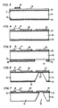
- FIGS. 3-11 An exemplary fabrication process of forming a silicon-based stripline laser mount will be described below in association with FIGS. 3-11. It is to be understood that this process is exemplary only and there exist various other techniques of creating the stripline mount structure depicted in FIG. 1. Further, although only one such mount is illustrated in the following figures, thousands of such mounts are actually being fabricated simultaneously on a single silicon wafer.
- a (100) silicon substrate 16 is formed so as to have a ⁇ 110> orientation as a lithographic reference, so as to aid in later steps in the fabrication process.
- a relatively thick oxide layer 30 is grown (or deposited) on top surface 17 of substrate 16.
- a thick oxide layer 32 is formed on bottom surface 15 of substrate 16. Oxide layers 30 and 32 may be formed simultaneously.
- a layer 34 of resistive material, tantalum nitride, for example, is next deposited to cover oxide layer 30.
- Layer 34 may be deposited utilizing plasma-enhanced chemical vapor deposition (PECVD) techniques to comprise a thickness of approximately 600 ⁇ .
- PECVD plasma-enhanced chemical vapor deposition
- the thickness of layer 34 is related to the relative range of resistivities required to perform impedance matching of the laser to the stripline, where Ta2N is known to comprise a resistivity of 64 ⁇ / ⁇ .
- a photoresist layer 35 is next deposited on resistance layer 34 so as to delineate the final position of the thin film matching resistor.
- FIG. 3 The structure of FIG. 3 is then illuminated and the exposed portions of resistance layer 34 are removed. Photoresist 35 is subsequently removed to uncover impedance matching resistor 14, as illustrated in FIG. 4.
- Metallic conductor areas 18,26 and 22 are next formed, where these areas may consist of tri-level structures of titanium, titanium nitride, and platinum; the titanium nitride being a relatively thin layer which is used to prevent the formation of the compound TiPt.
- the compound TiPt is resistant to etching and has been found to be problematic during subsequent operations.
- a layer of gold may then be deposited as the top layer of metal areas 18,26 and 22, where a thicker layer of gold is usually formed on areas 18 and 22 which will serve as wirebond pad sites.
- area 18, also referred to as first conductor 18, is used as a wirebond connection site between the external modulation current source (not shown) and section A of the transmission line.
- Metal area 26 defines the location of laser 12 and provides the bottom side (e.g., n-side) contact to laser 12.
- the connection to the top side of laser 12 (e.g., p-side) is provided by a wirebond between the top of laser 12 and metal contact 22, where metal contact 22 is coupled through metalized via 20 to the bottom conductive layer 24 of mount 10 (see FIG. 1).
- any of the wirebond connections mentioned in the present context may actually consist of a number of parallel wirebonds or ribbon bonds.
- the parasitic inductance of each separate bond results in further reducing the overall parasitic inductance, another important means for reducing the parasitic inductance of the interconnection network. This technique is applicable to all of the illustrated wirebonds.
- a layer of photoresist 40 is deposited to cover oxide layer 32, with an opening 42 defining the location of via 20, as illustrated in FIG. 5.
- the portion of oxide 32 exposed by photoresist 40 is subsequently removed with an appropriate etch.
- the exposed surface of silicon substrate 16 is then etched with a substance which, by virtue of the (100) plane of the substrate, will form an inverted V-groove structure as illustrated in FIG. 6. That is, the etching substance will cause the substrate to etch along the ⁇ 100> axis faster than the ⁇ III> axis, resulting in a pyramid structure bound by (111) planes.
- ethylenediamine pyrocatechol is one known compound which will form this inverted V-groove structure.
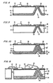
- Silicon dioxide layer 30 acts as an etch stop for this process. Once the substrate has been etched, portion 30′ of oxide layer 30 exposed by via 20, as well as oxide layer 32, are removed by an appropriate etch. The removal of portion 30′ of oxide layer 30 thus exposes metal contact area 22 to via 20, as shown in FIG. 7.
- the next step in the fabrication process is to form the metallized inner walls on via 20.
- the metallization is accomplished in two separate process sequences.
- a metal contact 44 is formed to cover the exposed bottom surface 15 of substrate 16, as well as covering the exposed sidewalls of via 20.
- metal contact 44 may consist of a first layer of titanium 41 and a second layer of platinum 43, each layer being sequentially sputtered onto the bottom surface of the structure, as illustrated in FIG. 8. In this case, no intermediate layer of titanium nitride is required, since this combination of layers will require no further etching. As shown in FIG.
- metal contact 44 is disposed to cover the inner walls of via 20 such that a portion of contact 44 (in this case, a portion of titanium layer 41) comes into direct contact with metal contact 22.
- This meeting of the two layers is extremely important, since the electrical coupling of layers 44 and 22 is required to provide the electrical connection to the top side of laser 12. It is to be noted that in the preferred arrangement, the bottom-most layer of metal contact 22 is also formed of titanium.
- a grinding (or polishing) operation is performed to reduce the overall thickness of substrate 16 (in actuality, the measured thickness defines the complete dielectric thickness of substrate 16 and overlying oxide layer 30).
- a thickness t of approximately 0.010 inches ( ⁇ 0.0001) is preferred and provides a stripline with an impedance of approximately 25 ⁇ .
- substrate 16 is initially formed to comprise the conventional wafer thickness of 0.020 inches, where all of the fabrication steps are performed on a wafer of this thickness.
- the substrate may be thinned to the appropriate value.
- FIG. 9 illustrates mount 10 subsequent to this thinning operation. As shown, the horizontal portions of metal contact 44 will be completely removed, but the walls of via 20 remain metalized, as denoted 44′ in FIG. 9.
- conductor 24 may consist of a tri-level structure including a first layer 48 of titanium, a second layer 50 of platinum and a third layer 52 of gold. If these layers are deposited by a conventional sputtering technique, layers 48,50 and 52 will cover not only exposed bottom surface 46, but will also fill in, to some extent, via 20.
- the wafer may be diced to separate the thousands of mounts so formed.
- the individual laser chips 12 are then mounted on metal contact 26 and the necessary wirebond connections are formed, as shown in FIG. 11.
Landscapes
- Physics & Mathematics (AREA)
- Condensed Matter Physics & Semiconductors (AREA)
- General Physics & Mathematics (AREA)
- Electromagnetism (AREA)
- Optics & Photonics (AREA)
- Semiconductor Lasers (AREA)
- Led Device Packages (AREA)
Applications Claiming Priority (2)
| Application Number | Priority Date | Filing Date | Title |
|---|---|---|---|
| US287778 | 1988-12-21 | ||
| US07/287,778 US4937660A (en) | 1988-12-21 | 1988-12-21 | Silicon-based mounting structure for semiconductor optical devices |
Publications (3)
| Publication Number | Publication Date |
|---|---|
| EP0375231A2 true EP0375231A2 (de) | 1990-06-27 |
| EP0375231A3 EP0375231A3 (en) | 1990-12-27 |
| EP0375231B1 EP0375231B1 (de) | 1994-10-12 |
Family
ID=23104310
Family Applications (1)
| Application Number | Title | Priority Date | Filing Date |
|---|---|---|---|
| EP89312877A Expired - Lifetime EP0375231B1 (de) | 1988-12-21 | 1989-12-11 | Silicium-Trägerstruktur für optische Halbleitervorrichtungen |
Country Status (6)
| Country | Link |
|---|---|
| US (1) | US4937660A (de) |
| EP (1) | EP0375231B1 (de) |
| JP (1) | JPH07114304B2 (de) |
| CA (1) | CA2005788C (de) |
| DE (1) | DE68918824T2 (de) |
| ES (1) | ES2060793T3 (de) |
Cited By (5)
| Publication number | Priority date | Publication date | Assignee | Title |
|---|---|---|---|---|
| EP0505842A1 (de) * | 1991-03-28 | 1992-09-30 | Alcatel SEL Aktiengesellschaft | Einrichtung mit einem Trägerteil, einem Halbleiterlaser und Zuleitungen |
| EP0579440A3 (de) * | 1992-07-15 | 1994-02-09 | AT&T Corp. | Verfahren zur Herstellung eines Aufbaus mit einem aus einem strukturierten Film bestehenden Träger und einem darauf selbstausgerichteten elektronischen Gerät |
| WO1998052255A1 (de) * | 1997-05-12 | 1998-11-19 | Robert Bosch Gmbh | Hochfrequenz-halbleiterlasermodul |
| WO1999062150A3 (de) * | 1998-05-27 | 2000-01-13 | Siemens Ag | Gehäuseanordnung für lasermodul |
| GB2386252A (en) * | 2001-12-06 | 2003-09-10 | Linear Techn Inc | Component containing light emitting and impedance elements |
Families Citing this family (13)
| Publication number | Priority date | Publication date | Assignee | Title |
|---|---|---|---|---|
| US5151776A (en) * | 1989-03-28 | 1992-09-29 | General Electric Company | Die attachment method for use in high density interconnected assemblies |
| US5061987A (en) * | 1990-01-09 | 1991-10-29 | Northrop Corporation | Silicon substrate multichip assembly |
| US5652460A (en) * | 1995-10-06 | 1997-07-29 | California Micro Devices Corporation | Integrated resistor networks having reduced cross talk |
| US5706163A (en) * | 1995-11-28 | 1998-01-06 | California Micro Devices Corporation | ESD-protected thin film capacitor structures |
| US5760662A (en) * | 1996-02-28 | 1998-06-02 | California Micro Devices Corporation | Methods and apparatus for improving frequency response of integrated RC filters with additional ground pins |
| US5706303A (en) * | 1996-04-09 | 1998-01-06 | Lawrence; Zachary Andrew | Laser diode coupling and bias circuit and method |
| US5982793A (en) * | 1996-05-20 | 1999-11-09 | Matsushita Electric Industrial Co., Ltd. | Semiconductor laser module with internal matching circuit |
| US6320706B1 (en) | 2000-02-24 | 2001-11-20 | Lightwave Electronics | Method and apparatus for positioning and fixating an optical element |
| US7151036B1 (en) * | 2002-07-29 | 2006-12-19 | Vishay-Siliconix | Precision high-frequency capacitor formed on semiconductor substrate |
| US6538300B1 (en) * | 2000-09-14 | 2003-03-25 | Vishay Intertechnology, Inc. | Precision high-frequency capacitor formed on semiconductor substrate |
| US7061949B1 (en) * | 2002-08-16 | 2006-06-13 | Jds Uniphase Corporation | Methods, apparatus, and systems with semiconductor laser packaging for high modulation bandwidth |
| JP4828103B2 (ja) * | 2004-07-28 | 2011-11-30 | 三菱電機株式会社 | 光送受信モジュール |
| CN114792928A (zh) * | 2021-01-25 | 2022-07-26 | 华为技术有限公司 | 激光器载体及其制作方法 |
Family Cites Families (12)
| Publication number | Priority date | Publication date | Assignee | Title |
|---|---|---|---|---|
| US3757259A (en) * | 1972-04-28 | 1973-09-04 | Us Army | Novel mounting technique for glass package diodes |
| JPS5137548A (en) * | 1974-09-26 | 1976-03-29 | Daiichi Denshi Kogyo | Dojikugatainpiidansuhenkanpatsudoyokaadoatsuteneeta narabini dojikugatainpiidansuhenkanpatsudo |
| GB1487010A (en) * | 1975-04-01 | 1977-09-28 | Standard Telephones Cables Ltd | Laser stud mounts |
| US4301429A (en) * | 1979-06-07 | 1981-11-17 | Raytheon Company | Microwave diode with high resistance layer |
| US4379273A (en) * | 1981-06-25 | 1983-04-05 | Mcdonnell Douglas Corporation | Pulse transformer laser diode package |
| JPS594175A (ja) * | 1982-06-30 | 1984-01-10 | Fujitsu Ltd | 電界効果半導体装置 |
| US4485361A (en) * | 1982-12-23 | 1984-11-27 | The United States Of America As Represented By The Secretary Of The Air Force | Pulse transformer package for impedance matching a laser diode to a transmission line |
| JPS59172787A (ja) * | 1983-03-22 | 1984-09-29 | Sharp Corp | 半導体レ−ザのサブマウント装置 |
| JPS6154674A (ja) * | 1984-08-25 | 1986-03-18 | Fujitsu Ltd | 超高周波集積回路装置 |
| US4761788A (en) * | 1985-10-28 | 1988-08-02 | American Telephone And Telegraph Company | Stripline mount for semiconductor lasers |
| JPS63104453A (ja) * | 1986-10-22 | 1988-05-09 | Hitachi Ltd | 半導体装置およびその製造方法 |
| JPS63110001U (de) * | 1987-01-08 | 1988-07-15 |
-
1988
- 1988-12-21 US US07/287,778 patent/US4937660A/en not_active Expired - Lifetime
-
1989
- 1989-12-11 DE DE68918824T patent/DE68918824T2/de not_active Expired - Fee Related
- 1989-12-11 EP EP89312877A patent/EP0375231B1/de not_active Expired - Lifetime
- 1989-12-11 ES ES89312877T patent/ES2060793T3/es not_active Expired - Lifetime
- 1989-12-18 CA CA002005788A patent/CA2005788C/en not_active Expired - Fee Related
- 1989-12-21 JP JP1329792A patent/JPH07114304B2/ja not_active Expired - Lifetime
Cited By (8)
| Publication number | Priority date | Publication date | Assignee | Title |
|---|---|---|---|---|
| EP0505842A1 (de) * | 1991-03-28 | 1992-09-30 | Alcatel SEL Aktiengesellschaft | Einrichtung mit einem Trägerteil, einem Halbleiterlaser und Zuleitungen |
| EP0579440A3 (de) * | 1992-07-15 | 1994-02-09 | AT&T Corp. | Verfahren zur Herstellung eines Aufbaus mit einem aus einem strukturierten Film bestehenden Träger und einem darauf selbstausgerichteten elektronischen Gerät |
| WO1998052255A1 (de) * | 1997-05-12 | 1998-11-19 | Robert Bosch Gmbh | Hochfrequenz-halbleiterlasermodul |
| WO1999062150A3 (de) * | 1998-05-27 | 2000-01-13 | Siemens Ag | Gehäuseanordnung für lasermodul |
| US6422766B1 (en) | 1998-05-27 | 2002-07-23 | Siemens Aktiengesellschaft Ag | Housing configuration for a laser module |
| GB2386252A (en) * | 2001-12-06 | 2003-09-10 | Linear Techn Inc | Component containing light emitting and impedance elements |
| FR2837059A1 (fr) * | 2001-12-06 | 2003-09-12 | Linear Techn Inc | Circuits et procedes pour ameliorer la performance d'un element emetteur de lumiere |
| GB2386252B (en) * | 2001-12-06 | 2005-05-04 | Linear Techn Inc | Circuitry and methods for improving the performance of a light emitting element |
Also Published As
| Publication number | Publication date |
|---|---|
| JPH02220491A (ja) | 1990-09-03 |
| ES2060793T3 (es) | 1994-12-01 |
| CA2005788A1 (en) | 1990-06-21 |
| CA2005788C (en) | 1993-06-22 |
| US4937660A (en) | 1990-06-26 |
| DE68918824T2 (de) | 1995-03-02 |
| DE68918824D1 (de) | 1994-11-17 |
| JPH07114304B2 (ja) | 1995-12-06 |
| EP0375231B1 (de) | 1994-10-12 |
| EP0375231A3 (en) | 1990-12-27 |
Similar Documents
| Publication | Publication Date | Title |
|---|---|---|
| US5024966A (en) | Method of forming a silicon-based semiconductor optical device mount | |
| EP0375231B1 (de) | Silicium-Trägerstruktur für optische Halbleitervorrichtungen | |
| US5463246A (en) | Large scale high density semiconductor apparatus | |
| US5648684A (en) | Endcap chip with conductive, monolithic L-connect for multichip stack | |
| US5063177A (en) | Method of packaging microwave semiconductor components and integrated circuits | |
| JP3947406B2 (ja) | 半導体レーザモジュール | |
| US5451818A (en) | Millimeter wave ceramic package | |
| JP2000012948A (ja) | 高周波レ―ザモジュ―ル、光電子素子および高周波レ―ザモジュ―ルの製造方法 | |
| JP2004356233A (ja) | 半導体レーザモジュールおよび半導体レーザ装置 | |
| JP2000353846A (ja) | ステム型半導体レーザ装置 | |
| US4996588A (en) | Device for interconnection and protection of a bare microwave component chip | |
| JPH09172221A (ja) | 光半導体素子の実装構造 | |
| US5160907A (en) | Multiple layer semiconductor circuit module | |
| JP7109454B2 (ja) | マルチビーム光電子アレイ用の整合性ドライブデバイス | |
| JP3823102B2 (ja) | 光伝送モジュール | |
| JP2002374028A (ja) | 配線基板 | |
| JP3434473B2 (ja) | 光モジュール用シリコンプラットフォーム | |
| JP3039463B2 (ja) | 半導体装置及びその製造方法 | |
| JP2003078196A (ja) | 光モジュール | |
| JP2000164970A (ja) | 光素子モジュール | |
| CN223297204U (zh) | 一种用于激光器芯片封装的基板 | |
| JP3769388B2 (ja) | 光半導体装置 | |
| JP2000114641A (ja) | 光半導体装置 | |
| JP2575382B2 (ja) | 集積回路装置 | |
| Müller et al. | Improved design options and microwave performance by combining thin film with LTCC |
Legal Events
| Date | Code | Title | Description |
|---|---|---|---|
| PUAI | Public reference made under article 153(3) epc to a published international application that has entered the european phase |
Free format text: ORIGINAL CODE: 0009012 |
|
| AK | Designated contracting states |
Kind code of ref document: A2 Designated state(s): DE ES FR GB NL |
|
| PUAL | Search report despatched |
Free format text: ORIGINAL CODE: 0009013 |
|
| AK | Designated contracting states |
Kind code of ref document: A3 Designated state(s): DE ES FR GB NL |
|
| 17P | Request for examination filed |
Effective date: 19910619 |
|
| 17Q | First examination report despatched |
Effective date: 19930629 |
|
| RAP3 | Party data changed (applicant data changed or rights of an application transferred) |
Owner name: AT&T CORP. |
|
| GRAA | (expected) grant |
Free format text: ORIGINAL CODE: 0009210 |
|
| AK | Designated contracting states |
Kind code of ref document: B1 Designated state(s): DE ES FR GB NL |
|
| ET | Fr: translation filed | ||
| REF | Corresponds to: |
Ref document number: 68918824 Country of ref document: DE Date of ref document: 19941117 |
|
| REG | Reference to a national code |
Ref country code: ES Ref legal event code: FG2A Ref document number: 2060793 Country of ref document: ES Kind code of ref document: T3 |
|
| PLBE | No opposition filed within time limit |
Free format text: ORIGINAL CODE: 0009261 |
|
| STAA | Information on the status of an ep patent application or granted ep patent |
Free format text: STATUS: NO OPPOSITION FILED WITHIN TIME LIMIT |
|
| 26N | No opposition filed | ||
| PGFP | Annual fee paid to national office [announced via postgrant information from national office to epo] |
Ref country code: NL Payment date: 20001130 Year of fee payment: 12 |
|
| PGFP | Annual fee paid to national office [announced via postgrant information from national office to epo] |
Ref country code: ES Payment date: 20001204 Year of fee payment: 12 |
|
| PGFP | Annual fee paid to national office [announced via postgrant information from national office to epo] |
Ref country code: FR Payment date: 20011121 Year of fee payment: 13 |
|
| PGFP | Annual fee paid to national office [announced via postgrant information from national office to epo] |
Ref country code: GB Payment date: 20011126 Year of fee payment: 13 |
|
| PGFP | Annual fee paid to national office [announced via postgrant information from national office to epo] |
Ref country code: DE Payment date: 20011230 Year of fee payment: 13 |
|
| REG | Reference to a national code |
Ref country code: GB Ref legal event code: IF02 |
|
| PG25 | Lapsed in a contracting state [announced via postgrant information from national office to epo] |
Ref country code: NL Free format text: LAPSE BECAUSE OF NON-PAYMENT OF DUE FEES Effective date: 20020701 |
|
| NLV4 | Nl: lapsed or anulled due to non-payment of the annual fee |
Effective date: 20020701 |
|
| PG25 | Lapsed in a contracting state [announced via postgrant information from national office to epo] |
Ref country code: GB Free format text: LAPSE BECAUSE OF NON-PAYMENT OF DUE FEES Effective date: 20021211 |
|
| PG25 | Lapsed in a contracting state [announced via postgrant information from national office to epo] |
Ref country code: ES Free format text: LAPSE BECAUSE OF NON-PAYMENT OF DUE FEES Effective date: 20021212 |
|
| PG25 | Lapsed in a contracting state [announced via postgrant information from national office to epo] |
Ref country code: DE Free format text: LAPSE BECAUSE OF NON-PAYMENT OF DUE FEES Effective date: 20030701 |
|
| GBPC | Gb: european patent ceased through non-payment of renewal fee | ||
| PG25 | Lapsed in a contracting state [announced via postgrant information from national office to epo] |
Ref country code: FR Free format text: LAPSE BECAUSE OF NON-PAYMENT OF DUE FEES Effective date: 20030901 |
|
| REG | Reference to a national code |
Ref country code: FR Ref legal event code: ST |
|
| REG | Reference to a national code |
Ref country code: ES Ref legal event code: FD2A Effective date: 20030113 |