EP0375247B1 - Einen metastabilen Zustand zulassende Kippschaltung - Google Patents
Einen metastabilen Zustand zulassende Kippschaltung Download PDFInfo
- Publication number
- EP0375247B1 EP0375247B1 EP89312956A EP89312956A EP0375247B1 EP 0375247 B1 EP0375247 B1 EP 0375247B1 EP 89312956 A EP89312956 A EP 89312956A EP 89312956 A EP89312956 A EP 89312956A EP 0375247 B1 EP0375247 B1 EP 0375247B1
- Authority
- EP
- European Patent Office
- Prior art keywords
- transistors
- transistor
- flip
- electrode
- output
- Prior art date
- Legal status (The legal status is an assumption and is not a legal conclusion. Google has not performed a legal analysis and makes no representation as to the accuracy of the status listed.)
- Expired - Lifetime
Links
- 230000004044 response Effects 0.000 claims description 3
- 230000008878 coupling Effects 0.000 claims 1
- 238000010168 coupling process Methods 0.000 claims 1
- 238000005859 coupling reaction Methods 0.000 claims 1
- 230000001629 suppression Effects 0.000 claims 1
- 230000008901 benefit Effects 0.000 description 6
- 230000007704 transition Effects 0.000 description 5
- 230000010355 oscillation Effects 0.000 description 4
- 238000010276 construction Methods 0.000 description 2
- 230000000694 effects Effects 0.000 description 2
- 238000005516 engineering process Methods 0.000 description 2
- 238000007667 floating Methods 0.000 description 2
- 230000009286 beneficial effect Effects 0.000 description 1
- 230000003247 decreasing effect Effects 0.000 description 1
- 238000010586 diagram Methods 0.000 description 1
- 230000001902 propagating effect Effects 0.000 description 1
- 238000011084 recovery Methods 0.000 description 1
- 230000001360 synchronised effect Effects 0.000 description 1
Images


Classifications
-
- H—ELECTRICITY
- H03—ELECTRONIC CIRCUITRY
- H03K—PULSE TECHNIQUE
- H03K3/00—Circuits for generating electric pulses; Monostable, bistable or multistable circuits
-
- H—ELECTRICITY
- H03—ELECTRONIC CIRCUITRY
- H03K—PULSE TECHNIQUE
- H03K3/00—Circuits for generating electric pulses; Monostable, bistable or multistable circuits
- H03K3/01—Details
- H03K3/013—Modifications of generator to prevent operation by noise or interference
-
- H—ELECTRICITY
- H03—ELECTRONIC CIRCUITRY
- H03K—PULSE TECHNIQUE
- H03K3/00—Circuits for generating electric pulses; Monostable, bistable or multistable circuits
- H03K3/02—Generators characterised by the type of circuit or by the means used for producing pulses
- H03K3/26—Generators characterised by the type of circuit or by the means used for producing pulses by the use, as active elements, of bipolar transistors with internal or external positive feedback
- H03K3/28—Generators characterised by the type of circuit or by the means used for producing pulses by the use, as active elements, of bipolar transistors with internal or external positive feedback using means other than a transformer for feedback
- H03K3/281—Generators characterised by the type of circuit or by the means used for producing pulses by the use, as active elements, of bipolar transistors with internal or external positive feedback using means other than a transformer for feedback using at least two transistors so coupled that the input of one is derived from the output of another, e.g. multivibrator
- H03K3/286—Generators characterised by the type of circuit or by the means used for producing pulses by the use, as active elements, of bipolar transistors with internal or external positive feedback using means other than a transformer for feedback using at least two transistors so coupled that the input of one is derived from the output of another, e.g. multivibrator bistable
- H03K3/287—Generators characterised by the type of circuit or by the means used for producing pulses by the use, as active elements, of bipolar transistors with internal or external positive feedback using means other than a transformer for feedback using at least two transistors so coupled that the input of one is derived from the output of another, e.g. multivibrator bistable using additional transistors in the feedback circuit
Definitions
- the present invention relates generally to latches and flip-flops, and more particularly relates to a flip-flop capable of suppressing and compensating for metastable conditions.
- Flip-flops are often used by system designers to synchronize signals operating at different frequencies to a local clock. However, since the signals are asynchronous to the local clock, the setup and hold time specifications associated with the flip-flop are sure to be violated. When the setup and hold time is violated, the output response of the flip-flop is uncertain.
- the output may assume a "metastable" state, defined as the time period during which the output of a digital logic device is not at logic level 1 or logic level 0, but instead resides at an output level between logic level 0 and logic level 1.
- the voltage ranges corresponding to different logic levels are specified by the manufacturer of the device. For bipolar TTL technology, for example, the metastable region might lie between 0.8 volts and 2.0 volts.
- the metastable problem occurs when the signal being input to the flip-flop is undergoing a transition from one logic level to the other simultaneously with the active edge of the local clock pulse, causing the latch section of the flip-flop to latch at an intermediate voltage level. Since the input data is changing while it is being clocked, the system designer does not care if the flip-flop goes to either a high or low logic level in this instance, just so long as the output does not "hang-up" in the metastable region. Neither level would be valid since the setup and hold was violated; so the actual result in this case is immaterial.
- the output of the flip-flop will stabilize at a valid logic level; however, logic circuitry following the flip-flop depends upon the delay specification (stated time period from the clock pulse to a valid output) being met. A metastable output may cause this logic circuitry to fail. Thus, the metastable characteristics of the flip-flop used to synchronize an asynchronous data stream can influence overall system reliability.
- the disclosed flip-flop suppresses and effectively compensates for the occurrence of metastable phenomena.
- the present invention provides a flip-flop circuit including, first and second input terminals and a clock input terminal, first and second output terminals, and first and second transistors each having first and second electrodes and a control electrode for controlling the conductance of the transistor between its first and second electrodes, the first and second input terminals being respectively connected to the control electrodes of the first and second transistors, the transistors being cross connected in that the there is a first feedback path from the first electrode of the first transistor to the control electrode of the second transistor and a second feedback path from the first electrode of the second transistor to the control electrode of the first transistor, the clock input terminal being connected to the second electrodes of the transistors, and the first and second output terminals being respectively connected to points on the second and first feedback paths, characterised in that the circuit includes means responsive to the voltage at the first electrode of the second transistor to interrupt the first feedback path at a point before the connection to the second output terminal and means responsive to the voltage
- the means may comprise output loading transistors coupled to the output terminals to ensure clamping of the cross coupled transistors.
- these transistors may be schottky transistors .
- Output glitch removal or suppressing circuitry may be added to the present invention to enhance its beneficial aspects.
- FIGUREs 1-5 of the drawings like numerals being used for like and-corresponding parts of the various drawings.
- FIGURE 1 illustrates the use of a D flip-flop to synchronize an asynchronous data stream.
- a D flip-flop 10 has a data input 11 receiving an asynchronous data stream 12.
- the output of a system clock 14 is also received by the clock input 15 of the D flop-flop 10.
- a synchrous data output 16 is transmitted from the terminal 17.
- the output 16 of the D flip-flop 10 is equal to the value of the asynchronous data stream 12 at the beginning of the clock pulse.
- the D flip-flop 10 outputs synchronized output data 16 which is equal to the asynchronous data stream 12 sampled at the system clock rate.
- the output of the D flip-flop 10 is valid after a specified time delay from the active edge of the clock pulse.
- the metastability problem occurs when the asynchronous data stream 12 is undergoing a transition between two logic levels fails the set up or hold time constraints with respect to the active edge of the system clock 14.
- the data stream is undergoing a logic low to logic high transition.
- the shaded region 18 represents the time period during which the asynchronous data stream 12 has not scttled into a valid logic level.
- the input data In order to ensure a valid output, the input data must be stable at a valid logic level for a time period represented by the setup time 20 and hold time 22 requirements.
- the setup time requirement 20 represents the time prior to the active edge of the clock pulse 24 during which the input data should be stable at a valid logic level.
- the hold time 22 represents the time period during which the input data must remain stable after the active edge of the clock pulse 24.
- the value of the output 16 is uncertain. While the output 16 may lock into a logical high or logical low value, it may also "hang up" at a voltage in the metastable region which is neither a logical high nor a logical low. Under conditions in which the setup and hold requirements 20 and 22 are met, a valid output will appear after a propagation time delay 26. However, if the output hangs up in the metastable region, an additional metastable time delay 28 is necessary before the output 16 assumes a valid logic level. It should be noted that since asynchronous data stream 12 is being sampled at a point between logic levels, either a logical high or logical low output is valid. It should also be noted that while the metastable time delay characteristic represents a time during which most metastable signals will lock into either a high or low logic level in most cases, it would still be possible for the output to hang up for periods greater than the metastable time delay 28.
- FIGURE 2b illustrates a signal which violates the setup and hold requirements during a logic high to logic low transition.
- FIGURE 3 illustrates a previously developed flip-flop circuit 30.
- the input 11 is connected to a bifurcating input section 31 which produces an inverted input 32 and non-inverted input 34, which are connected to a master latch section 35.
- the non-inverted input 34 is connected to the cathode of a first diode 36.
- the anode of the first diode 36 is connected to the base 38 of a first transistor 40 and to a resistor 42.
- the other lead of the resistor 42 is connected to a pullup resistor 44, the collector 46 of a second transistor 48, and a non-inverting output 50.
- the other lead of the pullup resistor 44 is connected to the power supply voltage, V cc 52.
- the inverting input 32 is connected to a cathode of a second diode 54.
- the anode of the second diode 54 is connected to the base 56 of the second transistor 48 and to a resistor 58.
- the other lead of the resistor 58 is connected to the collector 60 of the transistor 40, to a pullup resistor 62 and to an inverting output 64.
- the other lead of the pullup resistor 62 is connected to the power supply voltage, V cc 52.
- the emitters 66 and 68 of the transistors 40 and 48, respectively, are connected to an inverted clock 70, which is the inverted signal of the system clock 15.
- the non-inverted output 50 and inverted output 64 are connected to a slave latch output section 72.
- the system clock 15 is inverted in order to produce a falling edge in response to the active edge of the system clock. If the flip-flop is designed such that the falling edge is the active edge, no such inversion is necessary.
- the master section 35 comprises a latching circuit for locking in the values of the inverted and non-inverted inputs 32 and 34 at the time of the clock pulse.
- the slave output section 72 prevents false outputs from occurring when the inverted clock 70 is in a high state, by latching the outputs 50 and 64 at valid states.
- the slave output section can be implemented using two NAND gates, each having the output of the other as one input. The other inputs are supplied by the outputs 50 and 64 of the master section 35.
- the resistor combinations 42 and 44, and 58 and 62 are proportioned to divide the power supply voltage in a desired ratio.
- the resistors 42 and 58 should not be so large as to prevent the collectors 46 and 60 from drawing current therethrough.
- the input from the asynchronous data stream 11 is bifurcated into an inverted input 32 and a non-inverted input 34.
- the non-inverted input 34 has a logic high voltage
- the inverted input 32 has a logical low voltage.
- the voltage at the base 38 of the first transistor 40 is substantially higher than the voltage at the base 56 of the second transistor 48.
- the inverted clock signal 70 changes from a high to a low voltage
- the first transistor 40 turns on when the voltage differential between the base 38 and the inverted clock signal 70 exceeds the base-emitter threshold voltage, V be , of about .7 volts.
- the transistor 40 will turn on when the inverted clock 70 is at a voltage of 3.1 volts.
- the transistor 40 will conduct from collector 60 to emitter 66, drawing current away from the base 56 of the transistor 48.
- the second transistor 48 is prevented from turning on while the first transistor 40 is conducting.
- the metastability problem occurs when the asynchronous data stream is undergoing a transition during the active edge of the system clock signal 15. If the inverted input 32 and non-inverted input 34 have an equal voltage as the inverted clock signal 70 is decreasing, it is possible that both transistors 40 and 48 will turn on simultaneously. For example, if the bases 38 and 56 both have a voltage of 1.8 volts at precisely the time that the inverted clock signal 70 is at 1.1. volts, then both transistors will conduct simultaneously. Since neither transistor will be able to turn the other off, both inverted and non-inverted outputs 64 and 50 will have the same value, resulting in a metastable output. The transistors 40 and 48 will remain on until the system is perturbed by noise on one of the lines. At that point, one transistor will begin conducting more strongly than the other and will eventually draw enough current lorm the other transistor so as to turn the other transistor off.
- the present invention prevents metastable conditions occurring at the master portion from affecting the slave portion.
- the invention can be better understood by the following conceptual example, as applied to the prior art latch of FIGURE 3.
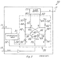
- the master section 74 of the present invention has similar construction to the master section 35 of the D flip-flop 30 previously described in connection with FIGURE 3, with the addition of transistors 76 and 78 coupled between the collectors of transistors 40 and 48 and resistors 100 and 102.
- transistor 76 has its emitter connected to the collector of transistor 48 and to the base of transistor 78.
- the collector of 76 is provided as Q output 1.
- Transistor 78 has its emitter connected to the collector of transistor 40 and to the base of transistor 76.
- the collector of 78 is provided as the Q ⁇ output 2.
- the respective bases of transistors 76 and 78 are also connected through pull up resistors 100 and 102 respectively to power supply voltage, V cc 52.
- the glitch removal circuit depicted in Fig. 5 can be connected between respective outputs 50 and 64 of master portion 74 and respective input 80 and 82 of slave portion 72.
- Glitch removal circuit 79 includes OR gate 92 having one input adapted to receive the Q ⁇ output of master portion 74, and another input having delay elements 88 and 90, such as inverters, serially connected to Q output 50.
- OR gate 104 connected between Q ⁇ output 64 of master portion 74 and input 82 of slave portion 72 is OR gate 104 having delay element 100 and 102 connected to one input and the other input connected directly to Q ⁇ output 64.
- the master section 74 of the present invention has been shown as an emitter-coupled cross latch, the invention works with any type latch which may assume an equilibrium state causing a metastable output.
- a technical advantage of the disclosed apparatus is that invalid metastable conditions can be prevented from propagating to the flip-flop output. This allows the flip-flop to hold steady until the next valid clock signal.
- Another technical advantage of the invention is that the output stage of the master can be clamped during a metastable occurrence at a voltage level insufficient to affect the slave portion of a master-slave flip-flop configuration.
- Another attendant advantage is that a valid output can be ensured after a definite time period, despite the occurrence of metastable conditions.
- the present invention is applicable to all types of flip-flops, including TTL, ECL, MOS, CMOS, and other technologies, and can be used with other flip-flop configurations, such as R-S flip-flops.
Landscapes
- Engineering & Computer Science (AREA)
- Power Engineering (AREA)
- Logic Circuits (AREA)
- Electronic Switches (AREA)
Claims (11)
- Flipflopschaltung miteinem ersten und einem zweiten Eingangsanschluß (34, 32) und einem Takteingangsanschluß (70),einem ersten und einem zweiten Ausgangsanschluß (OUT1, OUT2) undeinem ersten und einem zweiten Transistor (40, 48) mit jeweils einer ersten und einer zweiten Elektrode (60, 66, 46, 68) und einer Steuerelektrode (38, 56) zum Steuern der Leitfähigkeit des Transistors zwischen seiner ersten und seiner zweiten Elektrode,wobei der erste und der zweite Eingangsanschluß (34, 32) mit der Steuerelektrode des ersten bzw. des zweiten Transistors (40, 48) verbunden sind,wobei die Transistoren kreuzweise so verbunden sind, daß ein Rückkopplungsweg von der ersten Elektrode (60) des ersten Transistors (40) zur Steuerelektrode (56) des zweiten Transistors (48) und ein zweiter Rückkopplungsweg von der ersten Elektrode (46) des zweiten Transistors (48) zur Steuerelektrode (38) des ersten Transistors (40) vorhanden ist,wobei der Takteinangansanschluß (70) mit den zweiten Elektroden (66, 68) der Transistoren verbunden ist, undwobei der erste und der zweite Ausgangsanschluß (OUT1, OUT2) jeweils mit einem Punkt am zweiten bzw. ersten Rückkopplungsweg verbunden sind,dadurch gekennzeichnet, daß die Schaltung ein Mittel (78) enthält, das abhängig von der Spannung an der ersten Elektrode (46) des zweiten Transistors (48) den Rückkopplungsweg an einem Punkt vor der Verbindung mit dem zweiten Ausgangsanschluß (OUT2) unterbricht, sowie ein Mittel (76) enthält, das abhängig von der Spannung an der ersten Elektrode (60) des ersten Transistors (40) den zweiten Rückkopplungsweg an einem Punkt vor der Verbindung mit dem ersten Ausgangsanschluß (OUT1) unterbricht.
- Flipflopschaltung nach Anspruch 1, bei welcher das Mittel einen ersten und einen zweiten Lasttransistor (76, 78) mit jeweils einer Steuerelektrode und einer zweiten Elektrode sowie zwei Spannungsteilerschaltungen (42, 44 und 58, 60) zum selektiven Verbinden der ersten Elektrode jedes der ersten und zweiten Transistoren (40, 48) mit der Steuerelektrode des jeweils anderen der ersten und zweiten Transistoren und mit einem der Ausgangsanschlüsse (OUT1, OUT2) umfaßt, wobei die Steuerelektroden des ersten und des zweiten Lasttransistors an eine Referenzspannung gelegt sind, die erste Elektrode der gesteuerten Strombahn des ersten und des zweiten Lasttransistors (76, 78) mit einer jeweiligen ersten Elektrode des ersten und des zweiten Transistors (40, 48) und mit der Steuerelektrode des anderen Lasttransistors verbunden ist, und die zweite Elektrode des ersten und des zweiten Lasttransistors (76, 78) mit einem der Ausgangsanschlüsse (OUT1, OUT2) und mit den Spannungsteilerschaltungen (42, 44 und 58, 62) verbunden ist.
- Flipflopschaltung nach Anspruch 2, bei welcher die Spannungsteilerschaltungen enthalten:einen ersten Widerstand (44), der eine Referenzspannung (Vcc) an die zweite Elektrode des ersten Lasttransistors (76), an den mit der zweiten Elektrode des ersten Lasttransistors (76) verbundenen Ausgangsanschluß (OUT1) und an eine erste Klemme eines zweiten Widerstands (42) anlegt;eine erste Diode (36), die eine erste Eingangssignalleitung (34) mit einer zweiten Klemme des zweiten Widerstands (42) und mit der Steuerelektrode des ersten Transistors (40) verbindet;einen dritten Widerstand (62), der die Referenzspannung (Vcc) an die zweite Elektrode des zweiten Lasttransistors (78), an den mit der zweiten Elektrode des zweiten Lasttransistors (78) verbundenen Ausgangsanschluß (OUT2) und an eine erste Klemme eines vierten Widerstands (58) anlegt; undeine zweite Diode (54), die eine zweite Eingangssignalleitung (32) mit einer zweiten Klemme des vierten Widerstands (58) und mit der Steuerelektrode des zweiten Transistors (48) verbindet.
- Flipflopschaltung nach Anspruch 1, 2 oder 3, bei welcher die Steuerelektrode des ersten oder des zweiten Transistors (40, 48) so angeschlossen ist, daß sie ein invertiertes Eingangssignal enthält und die Steuerelektrode des anderen der Transistoren so angeschlossen ist, daß sie ein nicht invertiertes Eingangssignal empfängt.
- Flipflopschaltung nach Anspruch 2, bei welcher der erste und der zweite Lasttransistor (76, 78) Schottky-Transistoren sind.
- Flipflopschaltung nach Anspruch 5, bei welcher das Mittel die Spannungen an den Ausgangsanschlüssen (OUT1, OUT2) abhängig davon, daß die Eingangssignale gleiche Spannungen haben, auf einem konstanten Wert hält.
- Flipflopschaltung nach einem der vorhergehenden Ansprüche, ferner enthaltend eine SLAVE-Speicher-Flipflopschaltung (72), die mit den Ausgangsanschlüssen (OUT1, OUT2) verbunden ist.
- Flipflopschaltung nach Anspruch 7, ferner enthaltend eine erste und eine zweite Störimpulsunterdrückungsschaltung (Fig. 5), die jeweils die Ausgangsanschlüsse (OUT1, OUT2) mit der SLAVE-Speicher-Flipflopschaltung (72) koppeln.
- Flipflopschaltung nach Anspruch 6, bei welcher der konstante Wert ein gültiger Logikpegel ist.
- Flipflopschaltung nach Anspruch 9, bei welcher der gültige Logikpegel ein hoher Logikpegel ist.
- Flipflopschaltung nach Anspruch 9, bei welcher der gültige Logikpegel ein niedriger Logikpegel ist.
Applications Claiming Priority (2)
| Application Number | Priority Date | Filing Date | Title |
|---|---|---|---|
| US28854588A | 1988-12-21 | 1988-12-21 | |
| US288545 | 1988-12-21 |
Publications (3)
| Publication Number | Publication Date |
|---|---|
| EP0375247A2 EP0375247A2 (de) | 1990-06-27 |
| EP0375247A3 EP0375247A3 (de) | 1991-07-31 |
| EP0375247B1 true EP0375247B1 (de) | 1996-02-28 |
Family
ID=23107586
Family Applications (1)
| Application Number | Title | Priority Date | Filing Date |
|---|---|---|---|
| EP89312956A Expired - Lifetime EP0375247B1 (de) | 1988-12-21 | 1989-12-12 | Einen metastabilen Zustand zulassende Kippschaltung |
Country Status (5)
| Country | Link |
|---|---|
| US (1) | US5485112A (de) |
| EP (1) | EP0375247B1 (de) |
| JP (1) | JP2887898B2 (de) |
| KR (1) | KR0160954B1 (de) |
| DE (1) | DE68925799T2 (de) |
Families Citing this family (8)
| Publication number | Priority date | Publication date | Assignee | Title |
|---|---|---|---|---|
| US5789945A (en) * | 1996-02-27 | 1998-08-04 | Philips Electronics North America Corporation | Method and circuit for improving metastable resolving time in low-power multi-state devices |
| US5754070A (en) * | 1996-11-19 | 1998-05-19 | Vlsi Technology, Inc. | Metastableproof flip-flop |
| US6642763B2 (en) * | 2001-12-19 | 2003-11-04 | Intel Corporation | Long setup flip-flop for improved synchronization capabilities |
| US6986748B2 (en) * | 2002-08-15 | 2006-01-17 | Scimed Life Systems, Inc. | Multiple biopsy apparatus and related method of use |
| US7634749B1 (en) * | 2005-04-01 | 2009-12-15 | Cadence Design Systems, Inc. | Skew insensitive clocking method and apparatus |
| US7977975B1 (en) * | 2009-09-18 | 2011-07-12 | Altera Corporation | Apparatus for using metastability-hardened storage circuits in logic devices and associated methods |
| US8904336B1 (en) * | 2013-06-29 | 2014-12-02 | Synopsys, Inc. | Determination of meta-stable latch bias voltages |
| CN107276587B (zh) * | 2017-08-16 | 2020-04-14 | 电子科技大学 | 一种具有外部同步功能的振荡器电路 |
Family Cites Families (32)
| Publication number | Priority date | Publication date | Assignee | Title |
|---|---|---|---|---|
| US3292014A (en) * | 1965-01-11 | 1966-12-13 | Hewlett Packard Co | Logic circuit having inductive elements to improve switching speed |
| US3474263A (en) * | 1966-06-28 | 1969-10-21 | Texas Instruments Inc | Floating latch |
| US3591856A (en) * | 1967-11-07 | 1971-07-06 | Texas Instruments Inc | J-k master-slave flip-flop |
| US3558931A (en) * | 1968-04-05 | 1971-01-26 | Westinghouse Electric Corp | Flip-flop circuit particularly for integration |
| US3796831A (en) * | 1972-11-13 | 1974-03-12 | Rca Corp | Pulse modulation and detection communications system |
| US3835336A (en) * | 1973-03-23 | 1974-09-10 | Rca Corp | Pulse width sensing circuit |
| US3849673A (en) * | 1973-11-09 | 1974-11-19 | Bell Telephone Labor Inc | Compensated igfet flip-flop amplifiers |
| US3971960A (en) * | 1975-03-05 | 1976-07-27 | Motorola, Inc. | Flip-flop false output rejection circuit |
| US4150392A (en) * | 1976-07-31 | 1979-04-17 | Nippon Gakki Seizo Kabushiki Kaisha | Semiconductor integrated flip-flop circuit device including merged bipolar and field effect transistors |
| JPS5329057A (en) * | 1976-08-30 | 1978-03-17 | Nec Corp | Master slave type flip flop circuit |
| US4093878A (en) * | 1976-11-29 | 1978-06-06 | Ncr Corporation | De-glitchablenon-metastable flip-flop circuit |
| JPS53114651A (en) * | 1977-03-17 | 1978-10-06 | Fujitsu Ltd | Electronic circuit |
| JPS5544228A (en) * | 1978-09-25 | 1980-03-28 | Hitachi Ltd | Flip flop |
| JPS5632824A (en) * | 1979-08-24 | 1981-04-02 | Mitsubishi Electric Corp | Pulse eliminating circuit |
| DE3364452D1 (de) * | 1982-01-20 | 1986-08-21 | Matsushita Electric Industrial Co Ltd | Fet circuits |
| US4491745A (en) * | 1982-08-12 | 1985-01-01 | Motorola, Inc. | TTL flip-flop with clamping diode for eliminating race conditions |
| US4591737A (en) * | 1982-12-13 | 1986-05-27 | Advanced Micro Devices, Inc. | Master-slave multivibrator with improved metastable response characteristic |
| US4583008A (en) * | 1983-02-25 | 1986-04-15 | Harris Corporation | Retriggerable edge detector for edge-actuated internally clocked parts |
| US4578599A (en) * | 1983-06-02 | 1986-03-25 | Motorola, Inc. | Flip-flop having improved synchronous reset |
| US4517475A (en) * | 1983-08-29 | 1985-05-14 | Motorola, Inc. | Master-slave flip-flop arrangement with slave section having a faster output transistion and a greater resistance to output degradation |
| DE3407509A1 (de) * | 1984-03-01 | 1985-09-05 | A. Nattermann & Cie GmbH, 5000 Köln | Neue arzneimittelkombination zur behandlung von bluthochdruck und thromboembolischen erkrankungen |
| US4622475A (en) * | 1984-03-05 | 1986-11-11 | Tektronix, Inc. | Data storage element having input and output ports isolated from regenerative circuit |
| JPS60230714A (ja) * | 1984-04-28 | 1985-11-16 | Fujitsu Ltd | マスタ・スレ−ブ・フリツプフロツプ回路 |
| US4710648A (en) * | 1984-05-09 | 1987-12-01 | Hitachi, Ltd. | Semiconductor including signal processor and transient detector for low temperature operation |
| US4771187A (en) * | 1985-05-17 | 1988-09-13 | Nec Corporation | Bistable circuit |
| US4719366A (en) * | 1985-10-11 | 1988-01-12 | Advanced Micro Devices, Inc. | Output state protection network for D-type flip-flop |
| US4777388A (en) * | 1986-04-24 | 1988-10-11 | Tektronix, Inc. | Fast latching flip-flop |
| US4855617A (en) * | 1986-12-19 | 1989-08-08 | Texas Instruments Incorporated | Schottky transistor logic floating latch flip-flop |
| US4800296A (en) * | 1987-05-05 | 1989-01-24 | Texas Instruments Incorporated | Metastable defeating fli-flop |
| JPS63290046A (ja) * | 1987-05-21 | 1988-11-28 | Pioneer Electronic Corp | パルス幅ひずみ補正回路 |
| US4929850A (en) * | 1987-09-17 | 1990-05-29 | Texas Instruments Incorporated | Metastable resistant flip-flop |
| US4820939A (en) * | 1987-11-24 | 1989-04-11 | National Semiconductor Corporation | Finite metastable time synchronizer |
-
1989
- 1989-12-12 EP EP89312956A patent/EP0375247B1/de not_active Expired - Lifetime
- 1989-12-12 DE DE68925799T patent/DE68925799T2/de not_active Expired - Fee Related
- 1989-12-20 KR KR1019890019006A patent/KR0160954B1/ko not_active Expired - Fee Related
- 1989-12-20 JP JP1328551A patent/JP2887898B2/ja not_active Expired - Fee Related
-
1994
- 1994-07-28 US US08/278,715 patent/US5485112A/en not_active Expired - Lifetime
Also Published As
| Publication number | Publication date |
|---|---|
| JPH02218211A (ja) | 1990-08-30 |
| KR0160954B1 (ko) | 1999-03-20 |
| JP2887898B2 (ja) | 1999-05-10 |
| EP0375247A2 (de) | 1990-06-27 |
| DE68925799T2 (de) | 1996-07-11 |
| KR900011143A (ko) | 1990-07-11 |
| DE68925799D1 (de) | 1996-04-04 |
| US5485112A (en) | 1996-01-16 |
| EP0375247A3 (de) | 1991-07-31 |
Similar Documents
| Publication | Publication Date | Title |
|---|---|---|
| US4929850A (en) | Metastable resistant flip-flop | |
| KR940005506B1 (ko) | 플립플롭회로 | |
| US5543735A (en) | Method of controlling signal transfer between self-resetting logic circuits | |
| KR101374916B1 (ko) | 클럭 에지 복원을 갖는 펄스 카운터 | |
| US5867049A (en) | Zero setup time flip flop | |
| CA1290406C (en) | Finite metastable time synchronizer | |
| EP0477706B1 (de) | Schaltung zum Synchronisieren von asynchronen Zustandsmaschinen | |
| US6703881B2 (en) | Flip-flop circuit | |
| EP0375247B1 (de) | Einen metastabilen Zustand zulassende Kippschaltung | |
| US4435654A (en) | Output level adjustment means for low fanout ECL lacking emitter follower output | |
| US4282489A (en) | Metastable detector | |
| US6204708B1 (en) | Apparatus and method for an improved master-slave flip-flop with non-overlapping clocks | |
| US4651038A (en) | Gate having temperature-stabilized delay | |
| US4800296A (en) | Metastable defeating fli-flop | |
| CA1281088C (en) | Dynamic cmos current surge control | |
| US5391935A (en) | Assertive latching flip-flop | |
| US3679915A (en) | Polarity hold latch with common data input-output terminal | |
| US4274017A (en) | Cascode polarity hold latch having integrated set/reset capability | |
| JP2831788B2 (ja) | フリップフロップ回路 | |
| JPS61101113A (ja) | フリツプフロツプ回路 | |
| JP2870629B2 (ja) | 論理回路 | |
| US4578599A (en) | Flip-flop having improved synchronous reset | |
| US3845330A (en) | Bistable electronic circuit | |
| EP0523747A1 (de) | Verriegelungsschaltung | |
| US6683479B2 (en) | Multiphase comparator |
Legal Events
| Date | Code | Title | Description |
|---|---|---|---|
| PUAI | Public reference made under article 153(3) epc to a published international application that has entered the european phase |
Free format text: ORIGINAL CODE: 0009012 |
|
| AK | Designated contracting states |
Kind code of ref document: A2 Designated state(s): DE FR GB IT NL |
|
| PUAL | Search report despatched |
Free format text: ORIGINAL CODE: 0009013 |
|
| AK | Designated contracting states |
Kind code of ref document: A3 Designated state(s): DE FR GB IT NL |
|
| 17P | Request for examination filed |
Effective date: 19920114 |
|
| 17Q | First examination report despatched |
Effective date: 19931130 |
|
| GRAA | (expected) grant |
Free format text: ORIGINAL CODE: 0009210 |
|
| ITF | It: translation for a ep patent filed | ||
| AK | Designated contracting states |
Kind code of ref document: B1 Designated state(s): DE FR GB IT NL |
|
| REF | Corresponds to: |
Ref document number: 68925799 Country of ref document: DE Date of ref document: 19960404 |
|
| ET | Fr: translation filed | ||
| PLBE | No opposition filed within time limit |
Free format text: ORIGINAL CODE: 0009261 |
|
| STAA | Information on the status of an ep patent application or granted ep patent |
Free format text: STATUS: NO OPPOSITION FILED WITHIN TIME LIMIT |
|
| 26N | No opposition filed | ||
| REG | Reference to a national code |
Ref country code: GB Ref legal event code: IF02 |
|
| PGFP | Annual fee paid to national office [announced via postgrant information from national office to epo] |
Ref country code: NL Payment date: 20041111 Year of fee payment: 16 |
|
| PGFP | Annual fee paid to national office [announced via postgrant information from national office to epo] |
Ref country code: FR Payment date: 20041201 Year of fee payment: 16 |
|
| PGFP | Annual fee paid to national office [announced via postgrant information from national office to epo] |
Ref country code: DE Payment date: 20041230 Year of fee payment: 16 |
|
| PG25 | Lapsed in a contracting state [announced via postgrant information from national office to epo] |
Ref country code: IT Free format text: LAPSE BECAUSE OF NON-PAYMENT OF DUE FEES;WARNING: LAPSES OF ITALIAN PATENTS WITH EFFECTIVE DATE BEFORE 2007 MAY HAVE OCCURRED AT ANY TIME BEFORE 2007. THE CORRECT EFFECTIVE DATE MAY BE DIFFERENT FROM THE ONE RECORDED. Effective date: 20051212 |
|
| PG25 | Lapsed in a contracting state [announced via postgrant information from national office to epo] |
Ref country code: NL Free format text: LAPSE BECAUSE OF NON-PAYMENT OF DUE FEES Effective date: 20060701 Ref country code: DE Free format text: LAPSE BECAUSE OF NON-PAYMENT OF DUE FEES Effective date: 20060701 |
|
| PG25 | Lapsed in a contracting state [announced via postgrant information from national office to epo] |
Ref country code: FR Free format text: LAPSE BECAUSE OF NON-PAYMENT OF DUE FEES Effective date: 20060831 |
|
| NLV4 | Nl: lapsed or anulled due to non-payment of the annual fee |
Effective date: 20060701 |
|
| PGFP | Annual fee paid to national office [announced via postgrant information from national office to epo] |
Ref country code: GB Payment date: 20061106 Year of fee payment: 18 |
|
| REG | Reference to a national code |
Ref country code: FR Ref legal event code: ST Effective date: 20060831 |
|
| GBPC | Gb: european patent ceased through non-payment of renewal fee |
Effective date: 20071212 |
|
| PG25 | Lapsed in a contracting state [announced via postgrant information from national office to epo] |
Ref country code: GB Free format text: LAPSE BECAUSE OF NON-PAYMENT OF DUE FEES Effective date: 20071212 |