EP0375251B1 - Methode des Aufbaus eines optoelektronischen Gehäuses und Vorrichtung - Google Patents
Methode des Aufbaus eines optoelektronischen Gehäuses und Vorrichtung Download PDFInfo
- Publication number
- EP0375251B1 EP0375251B1 EP89312976A EP89312976A EP0375251B1 EP 0375251 B1 EP0375251 B1 EP 0375251B1 EP 89312976 A EP89312976 A EP 89312976A EP 89312976 A EP89312976 A EP 89312976A EP 0375251 B1 EP0375251 B1 EP 0375251B1
- Authority
- EP
- European Patent Office
- Prior art keywords
- angle
- monocrystalline
- optoelectronic device
- optical fiber
- further characterized
- Prior art date
- Legal status (The legal status is an assumption and is not a legal conclusion. Google has not performed a legal analysis and makes no representation as to the accuracy of the status listed.)
- Expired - Lifetime
Links
- 230000005693 optoelectronics Effects 0.000 title claims description 34
- 238000000034 method Methods 0.000 title claims description 14
- 239000013307 optical fiber Substances 0.000 claims description 39
- 229910052710 silicon Inorganic materials 0.000 claims description 26
- 239000010703 silicon Substances 0.000 claims description 26
- 238000005530 etching Methods 0.000 claims description 18
- 230000003287 optical effect Effects 0.000 claims description 12
- 229910021421 monocrystalline silicon Inorganic materials 0.000 claims description 11
- 230000000873 masking effect Effects 0.000 claims description 8
- 230000005540 biological transmission Effects 0.000 claims description 7
- 239000013078 crystal Substances 0.000 claims description 5
- XUIMIQQOPSSXEZ-UHFFFAOYSA-N Silicon Chemical compound [Si] XUIMIQQOPSSXEZ-UHFFFAOYSA-N 0.000 description 16
- 239000000835 fiber Substances 0.000 description 14
- VYPSYNLAJGMNEJ-UHFFFAOYSA-N Silicium dioxide Chemical compound O=[Si]=O VYPSYNLAJGMNEJ-UHFFFAOYSA-N 0.000 description 10
- 238000004891 communication Methods 0.000 description 7
- 230000008878 coupling Effects 0.000 description 7
- 238000010168 coupling process Methods 0.000 description 7
- 238000005859 coupling reaction Methods 0.000 description 7
- 235000012239 silicon dioxide Nutrition 0.000 description 5
- 239000000377 silicon dioxide Substances 0.000 description 5
- PCHJSUWPFVWCPO-UHFFFAOYSA-N gold Chemical compound [Au] PCHJSUWPFVWCPO-UHFFFAOYSA-N 0.000 description 3
- 239000010931 gold Substances 0.000 description 3
- 229910052737 gold Inorganic materials 0.000 description 3
- 239000004065 semiconductor Substances 0.000 description 3
- VYZAMTAEIAYCRO-UHFFFAOYSA-N Chromium Chemical compound [Cr] VYZAMTAEIAYCRO-UHFFFAOYSA-N 0.000 description 2
- 239000004593 Epoxy Substances 0.000 description 2
- KRHYYFGTRYWZRS-UHFFFAOYSA-N Fluorane Chemical compound F KRHYYFGTRYWZRS-UHFFFAOYSA-N 0.000 description 2
- YCIMNLLNPGFGHC-UHFFFAOYSA-N catechol Chemical compound OC1=CC=CC=C1O YCIMNLLNPGFGHC-UHFFFAOYSA-N 0.000 description 2
- 229910052804 chromium Inorganic materials 0.000 description 2
- 239000011651 chromium Substances 0.000 description 2
- 229910052681 coesite Inorganic materials 0.000 description 2
- 239000004020 conductor Substances 0.000 description 2
- 229910052906 cristobalite Inorganic materials 0.000 description 2
- 239000000463 material Substances 0.000 description 2
- 238000001465 metallisation Methods 0.000 description 2
- 238000004806 packaging method and process Methods 0.000 description 2
- 229910052682 stishovite Inorganic materials 0.000 description 2
- 239000000126 substance Substances 0.000 description 2
- 229910052905 tridymite Inorganic materials 0.000 description 2
- PIICEJLVQHRZGT-UHFFFAOYSA-N Ethylenediamine Chemical compound NCCN PIICEJLVQHRZGT-UHFFFAOYSA-N 0.000 description 1
- 238000005452 bending Methods 0.000 description 1
- 239000011248 coating agent Substances 0.000 description 1
- 238000000576 coating method Methods 0.000 description 1
- 238000010276 construction Methods 0.000 description 1
- 229910021419 crystalline silicon Inorganic materials 0.000 description 1
- 230000001419 dependent effect Effects 0.000 description 1
- 238000011161 development Methods 0.000 description 1
- 229910052732 germanium Inorganic materials 0.000 description 1
- GNPVGFCGXDBREM-UHFFFAOYSA-N germanium atom Chemical compound [Ge] GNPVGFCGXDBREM-UHFFFAOYSA-N 0.000 description 1
- 230000010354 integration Effects 0.000 description 1
- 238000012544 monitoring process Methods 0.000 description 1
- 238000013021 overheating Methods 0.000 description 1
- 229920002120 photoresistant polymer Polymers 0.000 description 1
- 238000004544 sputter deposition Methods 0.000 description 1
- 238000012360 testing method Methods 0.000 description 1
Images


Classifications
-
- G—PHYSICS
- G02—OPTICS
- G02B—OPTICAL ELEMENTS, SYSTEMS OR APPARATUS
- G02B6/00—Light guides; Structural details of arrangements comprising light guides and other optical elements, e.g. couplings
- G02B6/24—Coupling light guides
- G02B6/42—Coupling light guides with opto-electronic elements
- G02B6/4201—Packages, e.g. shape, construction, internal or external details
- G02B6/4204—Packages, e.g. shape, construction, internal or external details the coupling comprising intermediate optical elements, e.g. lenses, holograms
- G02B6/4214—Packages, e.g. shape, construction, internal or external details the coupling comprising intermediate optical elements, e.g. lenses, holograms the intermediate optical element having redirecting reflective means, e.g. mirrors, prisms for deflecting the radiation from horizontal to down- or upward direction toward a device
Definitions
- This invention relates to lightwave communication apparatus and, more particularly, to methods for making packages for optoelectronic devices, such as light-emitting diodes (LEDs).
- LEDs light-emitting diodes
- Optical or lightwave communications systems are presently being intensively explored because of their promise for delivering greater quantities of information over a transmission medium than is possible with conventional electrical communications systems.
- a lightwave source such as a laser or an LED
- a transmission medium such as an optical fiber
- a detector such as a semiconductor photodetector.
- Optical couplers are commonly used between the source and the detector for operating on the transmitted information (e.g., monitoring, amplifying).
- Devices such as lasers, LEDs and photodetectors that operate both electronically and optically are known as optoelectronic devices.
- the supports for various optoelectronic devices and the reflecting surfaces may, for example, be defined in monocrystalline silicon by taking advantage of known anisotropic etching properties of silicon. Because silicon etches preferentially along predictable crystallographic planes, various grooves, cavities and alignment detents can be quickly and easily made with great precision by masking and etching various surfaces of monocrystalline silicon support structures.
- LEDs differ from semiconductor LEDs in that they emit tight from a junction periphery in a direction parallel to the junction; whereas, LEDs emit light in a direction transverse to the junction through the "top" of the device.
- LEDs are commonly used in conjunction with multi-mode optical fibers for providing data communications (e.g., communication between computers); whereas, lasers are commonly used in conjunction with single-mode optical fibers to provide voice and voice-related communications.
- LEDs emit light in the vertical direction
- LED packages are somewhat difficult to make because, for structural reasons, it is preferred that the optical fiber extend from the package in a horizontal direction. Bending the fiber 90° is poor practice for both structural and optical reasons.
- the LED package contain a reflector for changing the direction of the emitted light prior to transmission by the optical fiber (see e.g. DE-A-3 543 558, which discloses a package method and apparatus according to the preamble of present claims 1 and 10, respectively.)
- efficient coupling between an optoelectronic device and an optical fiber is obtained by using different monocrystalline elements of different crystallographic orientation for mounting, respectively, the fiber and the optoelectronic device.
- the crystallographic orientation of an upper monocrystalline element is chosen such that a horizontal groove for supporting the optical fiber and a reflecting surface for directing fight into the fiber may both be made by anisotropic etching.
- the crystallographic orientation of a lower monocrystalline silicon element is chosen such that appropriate etching will yield a mounting surface for an optoelectronic device which is suitable for directing fight from the reflecting surface into the optical fiber with maximum efficiency.
- the upper monocrystalline element is ⁇ 100 ⁇ silicon
- the second monocrystalline element is ⁇ 112 ⁇ silicon.
- anisotropic etching so as to form a V-groove that supports a horizontally-extending optic fiber, a reflecting surface that extends at 54.74°, and a support surface for the optoelectronic device that extends at 19.48° with respect to the horizontal.
- These relative angles provide for optimum optical coupling between the optoelectronic device and the optical fiber, while providing horizontal surfaces for supporting both electronic circuitry and the optical fiber, as is desired for secure packaging and integration of the package apparatus into a lightwave communications system.
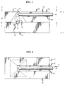
- the package 11 comprises an upper monocrystalline silicon element 17 and a lower monocrystalline silicon element 18, which have relative crystallographic orientations chosen to provide optimum mounting surfaces.
- a reflecting surface 19 is formed in the upper crystalline silicon element which is metallized, as is known in the art, so as to reflect light from the LED 13 into the fiber 15.
- the fiber 15 is contained within upper silicon element 17 by a V -groove 20 having side walls 21 that extend at 54.74° angles with the horizontal as shown.
- the upper silicon element 17 is ⁇ 100 ⁇ oriented monocrystalline silicon while the lower element is ⁇ 112 ⁇ monocrystalline silicon.
- the V -groove shown in FIG. 4 can easily be made by photolithographic masking and etching of the ⁇ 100 ⁇ element. That is, with all of element 17 masked, except for an opening in the upper surface 22 corresponding to the desired location of the groove as can he appreciated from FIG. 4, an etchant will preferentially etch along the ⁇ 111 ⁇ crystallographic planes so as to leave side walls 21 that correspond to such planes and are at 54.74° with respect to the horizontal.
- the element 17 is likewise masked with a rectangular opening in the lower surface of the mask.
- a polyhedron or pyramid of four surfaces is formed, with surface 19 having a slope at 54.74° with respect to the horizontal as a necessary consequence of the elements' crystallographic orientation.
- Surface 19 corresponds to the ⁇ 111 ⁇ plane.
- the ⁇ 112 ⁇ oriented silicon element 18 is masked except for an opening at its upper surface and etched so as to form a surface 23 which is parallel with the ⁇ 111 ⁇ crystallographic plane. It can be shown that one of the ⁇ 111 ⁇ planes in ⁇ 112 ⁇ oriented silicon is at an angle with respect to the horizontal of 19.48°.
- surface 23 After surface 23 has been formed, it is metallized, and LED 13 is mounted on it. With reflecting surface 19 extending at 54.74 degrees, the light projected normally with respect to surface 23 will be reflected from surface 19 in a direction parallel to the V -groove in element 17, and thus parallel to the central axis of optical fiber 15 as required for maximum coupling efficiency.
- FIG. 5 illustrates the relevant geometry.
- line 19' to extend at the same angle ⁇ with respect to the horizontal as does the reflecting surface 19 of FIG. 1.
- the exercise is to determine the angle ⁇ which accomplishes this desired result.
- ⁇ 1 ⁇ 2
- the lower silicon element 18 was stripped of its silicon dioxide, and a new oxide layer 0.1 micrometers thick was regrown.
- the sample was then coated by sputtering with a 0.03 micrometer thick layer of chromium, followed by a 0.2 micrometer thick layer of gold. Careful coating with photoresist and multiple exposures and development allowed a conductor pattern to be formed which preserved the metallization over the lip of the recess. After etching away the exposed gold and chromium, the sample was re-plated with gold to a 5 micrometer thickness. This extra thickness was provided to insure sufficient current-carrying capacity for the performance of the LED without overheating the conductors and to provide a good bonding pad for the LED.
- LEDs were epoxy bonded into the etched recesses and wire bonded.
- a simple jig was designed and fabricated to hold the surface 23 at a horizontal angle so that the LED could be positioned, epoxied, and wire bonded with standard equipment.
- Spherical lenses were epoxied onto the LEDs, and the submounts were attached to a header.
- the headers made convenient test vehicles for holding devices and making electrical connections.
- the upper monocrystalline element 17 is identical to a corresponding element described in U.S.-A-4,897,711 and so its construction will not be reviewed in detail.
- the masking and etching may proceed as generally described with respect to the lower element 18; that is, the same SiO 2 masking and etch and silicon etch may be used as described above.
- a lid may he included on the top surface 22 as generally described in U.S.-A-4,897,711.
- Various other mounting structures and electrical contacts may be made as generally described in the Blonder et al. patent application and elsewhere in the literature.
- the package of FIG. 1 provides for optimum optical coupling between the LED device 23 and the optical fiber 15, in a manner that is consistent with the use of a horizontally-extending V -groove for supporting the fiber and conventional metallization for making electrical contact to the LED 23.
- the final result is a package in which it is not necessary to bend the optical fiber to make it extend in a horizontal direction. This would not be true, for example, if the LED were made to be supported on a flat horizontal surface and the optical fiber extended axially in a vertical direction.
- the resulting 90° bend that would be required to bring the fiber to a horizontal position would be a source of mechanical stress, as well as optical transmission losses.
- Other designs could be configured in which the optical fiber extends at other angles from the package, but such configurations would normally be inferior to the ones shown in which the fiber extends in a horizontal direction.
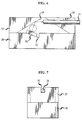
- FIGs. 6 and 7 illustrate an alternative embodiment of the invention comprising an upper monocrystalline silicon element 27 and a lower monocrystalline silicon element 28.
- the lower silicon element has a ⁇ 112 ⁇ crystallographic orientation which is essentially the same as the lower element 18 of FIG. 1, except that it has been rotated 180° with respect to the orientation shown in FIG. 1. Therefore, the effective angle ⁇ of mount surface 23' with respect to the horizontal is -19.48° rather than 19.48°.
- the upper silicon element 27 has a ⁇ 110 ⁇ orientation. With this orientation, etching from the bottom surface of element 27 will yield opposite sloping walls and opposite vertical walls.
- the reflector wall 29 will have an angle with respect to the horizontal of 35.26° which corresponds to a ⁇ 111 ⁇ crystallographic plane.
- the fiber groove is made by etching silicon element 27 from the top surface which, with the ⁇ 110 ⁇ orientation of element 27, yields the U -shaped groove 30 having a horizontal axis as shown in FIG. 6. With the U -shaped groove, of course, the fiber 31 will again extend in a horizontal direction.
- the vertical sidewalls of groove 30 correspond to the ⁇ 111 ⁇ planes.
- the LED 32 is mounted such as to project light that is reflected from reflecting surface 29 in a horizontal direction for optimum coupling into the optical fiber 31.
- the invention was stimulated by a need to provide optimum coupling between an LED and an optical fiber, it can he seen that it may be used in any optoelectronic device in which optimum coupling with a fiber is desired.
- the LEDs of FIGs. and 5 could he photodetectors which are optimally positioned by the package to receive light from the optical fiber. If lasers were made so as to emit light from the side opposite the side that is mounted on a support plane, then the invention would he applicable to such lasers. Silicon was chosen as the monocrystalline substance that seems to be the most practical for implementing the invention, but clearly other crystalline substances, such as germanium, could alternatively be used. While the relative angles obtained through etching are extremely precise, the absolute angles are dependent on the precision with which the monocrystalline elements were initially cut, as is known in the art.
Landscapes
- Physics & Mathematics (AREA)
- General Physics & Mathematics (AREA)
- Optics & Photonics (AREA)
- Optical Couplings Of Light Guides (AREA)
Claims (18)
- Verfahren zur Herstellung einer optoelektronischen Bauteilbaugruppe (11) umfassend die Schritte des Befestigens einer optischen Faser derart, daß sich diese in einer ersten Richtung axial erstreckt, Ausbilden einer ebenen reflektierenden Oberfläche (19) durch maskieren eines ersten monokristallinen Elementes (17) und dessen Ätzen zu einer ersten kristallographischen Ebene, Positionieren des ersten monokristallinen Elementes relativ zur optischen Faser so, daß sich die reflektierende Oberfläche (19) unter einem ersten Winkel α in Bezug auf die erste Richtung erstreckt, wobei der erste Winkel α ungleich 45° ist, Befestigen einer optoelektronischen Einrichtung 13 derart, daß ein optischer Weg zwischen der optoelektronischen Einrichtung und der optischen Faserachse durch die reflektierende Oberfläche beschrieben wird, gekennzeichnet durch
Ausbilden einer flachen Befestigungsfläche (23) für die optoelektronische Einrichtung durch Maskieren eines zweiten monokristallinen Elementes (18) und dessen Ätzen zu einer zweiten kristallographischen Ebene, wobei das zweite monokristalline Element (18) eine Kristallorientierung aufweist, die von derjenigen des ersten monokristallinen Elementes (17) verschieden ist, Befestigen des zweiten monokristallinen Elementes an dem ersten monokristallinen Element derart, daß die Befestigungsoberfläche sich unter einem zweiten Winkel β in Bezug auf die erste Richtung erstreckt, Befestigen der optischen Faser an einem der monokristallinen Elemente, um die erste Richtung zu den kristallographischen Richtungen des ersten und zweiten monokristallinen Elementes in Bezug zu setzen, und Befestigen der optoelektronischen Einrichtung an der Befestigungsoberfläche, um so die optoelektronische Einrichtung unter dem zweiten Winkel β zu orientieren, wobei die Kristallorientierung des zweiten monokristallinen Elementes in bezug auf diejenige des ersten monokristallinen Elementes so gewählt ist, daß der zweite Winkel β der Befestigungsoberfläche relativ zum ersten Winkel α der reflektierenden Oberfläche geeignet ist, um optische Übertragung entlang des optischen Weges zwischen der optoelektronischen Einrichtung und der optischen Faser bereitzustellen. - Verfahren nach Anspruch 1, ferner dadurch gekennzeichnet, daß der zweite Winkel β ungefähr gleich 2α - 90° ist, wobei α der erste Winkel ist.
- Verfahren nach Anspruch 2, ferner dadurch gekennzeichnet, daß:
der Schritt des Befestigens der optischen Faser den Schritt des Maskierens und Ätzens des ersten monokristallinen Elementes umfaßt, um so eine Furche (20), die durch kristallographische Ebenen definiert ist, auszubilden und dann das Befestigen der optischen Faser in der Furche umfaßt. - Verfahren nach Anspruch 3, ferner dadurch gekennzeichnet, daß:
das erste monokristalline Element {100}-Silizium ist, das zweite monokristalline Element {112}-Silizium ist, die erste kristallographische Ebene eine {111}-Ebene ist und die zweite kristallographische Ebene eine kristallographische {111}-Ebene ist. - Verfahren nach Anspruch 4, ferner dadurch gekennzeichnet, daß:
die optische Faser in einer durch {111}-Ebenen in dem ersten monokristallinen Siliziumelement definierten V-Furche befestigt ist. - Verfahren nach Anspruch 5, ferner dadurch gekennzeichnet, daß der erste Winkel α im wesentlichen 54,74° und der zweite Winkel β im wesentlichen 19,48° ist.
- Verfahren nach Anspruch 3, ferner dadurch gekennzeichnet, daß:
das erste monokristalline Element {110}-Silizium ist, das zweite monokristalline Element {112}-Silizium ist, die erste kristallographische Ebene eine {111}-Ebene und die zweite kristallographische Ebene eine {111}-Ebene ist. - Verfahren nach Anspruch 7, ferner dadurch gekennzeichnet, daß:
die optische Faser in einer durch kristallographische {111}-Ebenen in dem ersten monokristallinen Element definierten Furche befestigt ist. - Verfahren nach Anspruch 8, ferner dadurch gekennzeichnet, daß:
der erste Winkel α im wesentlichen 35,26° beträgt und der zweite Winkel β im wesentlichen -19,48° beträgt. - Optoelektronische Bauteilbaugruppe (11), umfassend eine optische Faser (15), die sich in einer ersten Richtung erstreckt, eine flache reflektierende Oberfläche (19), die durch eine erste kristallographische Ebene eines ersten monokristallinen Elementes (17) definiert ist, das relativ zur optischen Faser so angeordnet ist, daß die reflektierende Oberfläche sich unter einem ersten Winkel α in bezug auf die erste Richtung erstreckt, wobei der erste Winkel α nicht 45° ist, und enthaltend eine optoelektronische Einrichtung (13), die in einen optischen Weg einbezogen ist, der die Achse der optischen Faser und die reflektierende Oberfläche umfaßt, dadurch gekennzeichnet, daß:
die optoelektronische Einrichtung an einer ebenen Befestigungsfläche (23) befestigt ist, die durch eine zweite kristallographische Ebene eines zweiten monokristallinen Elementes (18) mit einer Kristallorientierung, die verschieden von derjenigen des ersten monokristallinen Elementes ist, definiert ist, wobei das zweite monokristalline Element an dem ersten monokristallinen Element derart befestigt ist, daß die Befestigungsfläche sich unter einem zweiten Winkel β relativ zur ersten Richtung erstreckt und die optische Faser an einem der monokristallinen Elemente befestigt ist, wobei sich diese in der ersten Richtung erstreckt, wobei die Kristallorientierung des zweiten monokristallinen Elementes relativ zu derjenigen des ersten monokristallinen Elementes so ausgewählt ist, daß der zweite Winkel β der Befestigungsfläche relativ zum ersten Winkel α der reflektierenden Oberfläche geeignet ist, die optische Übertragung entlang des optischen Weges zwischen der optoelektronischen Einrichtung und der optischen Faser bereitzustellen. - Optoelektronische Bauteilbaugruppe nach Anspruch 10, ferner dadurch gekennzeichnet, daß:
der zweite Winkel
- Optoelektronische Bauteilbaugruppe nach Anspruch 11, ferner dadurch gekennzeichnet, daß:
die optische Faser in einer Furche (20), die durch kristallographische Ebenen in dem ersten monokristallinen Element ausgebildet ist, befestigt ist. - Optoelektronische Bauteilbaugruppe nach Anspruch 12, ferner dadurch gekennzeichnet, daß:
das erste monokristalline Element {100}-Silizium ist, das zweite monokristalline Element {112}-Silizium ist, die erste kristallographische Ebene eine {111}-Ebene ist und die zweite kristallographische Ebene eine {111}-Ebene ist. - Optoelektronische Bauteilbaugruppe nach Anspruch 13, ferner dadurch gekennzeichnet, daß:
die optische Faser in einer durch {111}-Ebenen in dem ersten monokristallinen Siliziumelement ausgebildeten V-Furche enthalten ist. - Optoelektronische Bauteilbaugruppe nach Anspruch 14, ferner dadurch gekennzeichnet, daß:
der erste Winkel α im wesentlichen 54,74° und der zweite Winkel β im wesentlichen 19,48° beträgt. - Optoelektronische Bauteilbaugruppe nach Anspruch 12, ferner dadurch gekennzeichnet, daß:
das erste monokristalline Element {110}-Silizium ist, das zweite monokristalline Element {112}-Silizium ist, wobei die erste kristallographische Ebene eine {111}-Ebene ist und die zweite kristallographische Ebene eine {111}-Ebene ist. - Optoelektronische Bauteilbaugruppe nach Anspruch 16, ferner dadurch gekennzeichnet, daß:
die optische Faser in einer durch kristallographische {111}-Ebenen in dem ersten monokristallinen Element ausgebildeten Furche befestigt ist. - Optoelektronische Bauteilbaugruppe nach Anspruch 17, ferner dadurch gekennzeichnet, daß:
der erste Winkel α im wesentlichen 35,26° beträgt und der zweite Winkel β im wesentlichen -19,48° beträgt.
Applications Claiming Priority (3)
| Application Number | Priority Date | Filing Date | Title |
|---|---|---|---|
| US289093 | 1988-12-23 | ||
| US07/289,093 US5017263A (en) | 1988-12-23 | 1988-12-23 | Optoelectronic device package method |
| SG155694A SG155694G (en) | 1988-12-23 | 1994-10-21 | Optoelectronic device package method and apparatus |
Publications (3)
| Publication Number | Publication Date |
|---|---|
| EP0375251A2 EP0375251A2 (de) | 1990-06-27 |
| EP0375251A3 EP0375251A3 (de) | 1991-05-08 |
| EP0375251B1 true EP0375251B1 (de) | 1994-07-27 |
Family
ID=26664458
Family Applications (1)
| Application Number | Title | Priority Date | Filing Date |
|---|---|---|---|
| EP89312976A Expired - Lifetime EP0375251B1 (de) | 1988-12-23 | 1989-12-12 | Methode des Aufbaus eines optoelektronischen Gehäuses und Vorrichtung |
Country Status (5)
| Country | Link |
|---|---|
| US (1) | US5017263A (de) |
| EP (1) | EP0375251B1 (de) |
| JP (1) | JP2700010B2 (de) |
| DE (1) | DE68917108T2 (de) |
| SG (1) | SG155694G (de) |
Families Citing this family (21)
| Publication number | Priority date | Publication date | Assignee | Title |
|---|---|---|---|---|
| US5124281A (en) * | 1990-08-27 | 1992-06-23 | At&T Bell Laboratories | Method of fabricating a photonics module comprising a spherical lens |
| US5357103A (en) * | 1991-10-02 | 1994-10-18 | Sumitomo Electric Industries, Inc. | Light receiving module with optical fiber coupling |
| US5178723A (en) * | 1991-11-04 | 1993-01-12 | At&T Bell Laboratories | Method and apparatus for making optical devices |
| GB9203128D0 (en) * | 1992-02-14 | 1992-04-01 | Lucas Ind Plc | Alignment device for optical fibre |
| DE69416016T2 (de) * | 1993-02-23 | 1999-07-15 | The Whitaker Corp., Wilmington, Del. | Faseroptische Kopplungseinrichtung |
| JP2842132B2 (ja) * | 1993-03-05 | 1998-12-24 | 松下電器産業株式会社 | 光学デバイス |
| FR2707401B1 (fr) * | 1993-07-09 | 1995-08-11 | Menigaux Louis | Procédé de fabrication d'une structure intégrant un guide optique clivé à un support de fibre optique pour un couplage optique guide-fibre et structure obtenue. |
| DE4325955C2 (de) * | 1993-07-27 | 1997-09-11 | Siemens Ag | Verfahren zum Herstellen eines Halbleitersubstrats mit integriertem Wellenleiter und daran angekoppelter optischer Faser |
| US5589083A (en) * | 1993-12-11 | 1996-12-31 | Electronics And Telecommunications Research Institute | Method of manufacturing microstructure by the anisotropic etching and bonding of substrates |
| US5415730A (en) * | 1993-12-14 | 1995-05-16 | At&T Corp. | Metal coated optical fiber techniques |
| WO1997032344A1 (en) * | 1996-02-28 | 1997-09-04 | The Whitaker Corporation | Packaging for optoelectronic device |
| US5692083A (en) * | 1996-03-13 | 1997-11-25 | The Whitaker Corporation | In-line unitary optical device mount and package therefor |
| TW365057B (en) * | 1997-12-31 | 1999-07-21 | Ind Tech Res Inst | Manufacturing method for micro-mirror on the silicon substrate |
| DE10332651A1 (de) * | 2002-07-22 | 2004-02-26 | Forschungszentrum Karlsruhe Gmbh | Verfahren zur Herstellung von Photolackstrukturen |
| US20040022494A1 (en) * | 2002-08-05 | 2004-02-05 | Liddle James A. | Fiber optic array with fiber tap and methd for making and using |
| US20040047571A1 (en) * | 2002-09-06 | 2004-03-11 | Boord Warren Timothy | Hermetically sealed ferrule |
| KR100624405B1 (ko) * | 2002-10-01 | 2006-09-18 | 삼성전자주식회사 | 광부품 실장용 기판 및 그 제조방법 |
| US6945712B1 (en) | 2003-02-27 | 2005-09-20 | Xilinx, Inc. | Fiber optic field programmable gate array integrated circuit packaging |
| US6789959B1 (en) | 2003-02-27 | 2004-09-14 | Xilinx, Inc. | Fiber optic integrated circuit package using micromirrors |
| JP4631671B2 (ja) * | 2005-11-29 | 2011-02-16 | オムロン株式会社 | 光ケーブルモジュール、および光ケーブルモジュールを備える電子機器 |
| DE102013011581B4 (de) | 2013-07-04 | 2015-05-21 | Fraunhofer-Gesellschaft zur Förderung der angewandten Forschung e.V. | Anordnung aus einem Substrat mit mindestens einem optischen Wellenleiter und einer optischen Koppelstelle und aus einem optoelektronischen Bauelement und Verfahren zur Herstellung einer solchen Anordnung |
Citations (1)
| Publication number | Priority date | Publication date | Assignee | Title |
|---|---|---|---|---|
| DE3543558A1 (de) * | 1985-12-10 | 1987-06-11 | Licentia Gmbh | Opto-elektrische koppelanordnung |
Family Cites Families (5)
| Publication number | Priority date | Publication date | Assignee | Title |
|---|---|---|---|---|
| US4119363A (en) * | 1976-03-18 | 1978-10-10 | Bell Telephone Laboratories Incorporated | Package for optical devices including optical fiber-to-metal hermetic seal |
| US4357072A (en) * | 1978-01-28 | 1982-11-02 | Plessey Handel Und Investments Ag | Sealing optical fibres into packages |
| CA1108899A (en) * | 1978-08-17 | 1981-09-15 | Rca Limited | Light detector housing for fiber optic applications |
| JPS60172004A (ja) * | 1984-02-17 | 1985-09-05 | Fujitsu Ltd | 光受光器 |
| ATE50864T1 (de) * | 1985-10-16 | 1990-03-15 | British Telecomm | Fabry-perot-interferometer. |
-
1988
- 1988-12-23 US US07/289,093 patent/US5017263A/en not_active Expired - Fee Related
-
1989
- 1989-11-24 JP JP1303461A patent/JP2700010B2/ja not_active Expired - Fee Related
- 1989-12-12 EP EP89312976A patent/EP0375251B1/de not_active Expired - Lifetime
- 1989-12-12 DE DE68917108T patent/DE68917108T2/de not_active Expired - Fee Related
-
1994
- 1994-10-21 SG SG155694A patent/SG155694G/en unknown
Patent Citations (1)
| Publication number | Priority date | Publication date | Assignee | Title |
|---|---|---|---|---|
| DE3543558A1 (de) * | 1985-12-10 | 1987-06-11 | Licentia Gmbh | Opto-elektrische koppelanordnung |
Also Published As
| Publication number | Publication date |
|---|---|
| US5017263A (en) | 1991-05-21 |
| JP2700010B2 (ja) | 1998-01-19 |
| SG155694G (en) | 1995-03-17 |
| EP0375251A2 (de) | 1990-06-27 |
| DE68917108D1 (de) | 1994-09-01 |
| EP0375251A3 (de) | 1991-05-08 |
| DE68917108T2 (de) | 1994-11-10 |
| JPH02190804A (ja) | 1990-07-26 |
Similar Documents
| Publication | Publication Date | Title |
|---|---|---|
| US5073003A (en) | Optoelectronic device package method and apparatus | |
| EP0375251B1 (de) | Methode des Aufbaus eines optoelektronischen Gehäuses und Vorrichtung | |
| US6874950B2 (en) | Devices and methods for side-coupling optical fibers to optoelectronic components | |
| US5940562A (en) | Stubless optoelectronic device receptacle | |
| US7250317B2 (en) | Method of fabricating optical waveguide reflectors | |
| US7404679B2 (en) | Termination for optic fiber with improved optical features | |
| US8031993B2 (en) | Optical fiber interconnect device | |
| US12379555B2 (en) | Detachable connector for co-packaged optics | |
| JP2003207694A (ja) | 光モジュール | |
| EP0660146B1 (de) | Lichtempfängerstruktur für optische Vorrichtungen vom Wellenleitertyp | |
| US8542963B2 (en) | Method for manufacturing optical coupling element, optical transmission substrate, optical coupling component, coupling method, and optical interconnect system | |
| JPH0793457B2 (ja) | 光学素子の製造方法 | |
| JP2001324631A (ja) | 基板、光ファイバ接続端部材、光素子ハウジング部材、光モジュール及び基板の製造方法 | |
| JPH10126002A (ja) | 光伝送モジュール | |
| US6023546A (en) | Structure for securing optical device and fiber optics | |
| KR100211985B1 (ko) | 하이브리드 광집적회로용 마이크로 거울, 그의 제조방법, 마이크로 거울-광검출기 어셈블리 및 광수신용 하이브리드 광집적회로 어셈블리 | |
| JP3168297B2 (ja) | 光学素子取り付け方法 | |
| EP0846966A2 (de) | Optischer Wellenleiter | |
| US5224184A (en) | Optical multi-chip interconnect | |
| HK130595A (en) | Optoelectronic device package method and apparatus | |
| JP3202296B2 (ja) | 半導体レーザアレイとシングルモードファイバアレイとの光結合構造 | |
| KR20070023420A (ko) | 실리콘 광학 벤치를 이용한 광송수신 모듈 | |
| JPH10308528A (ja) | 光半導体モジュール |
Legal Events
| Date | Code | Title | Description |
|---|---|---|---|
| PUAI | Public reference made under article 153(3) epc to a published international application that has entered the european phase |
Free format text: ORIGINAL CODE: 0009012 |
|
| AK | Designated contracting states |
Kind code of ref document: A2 Designated state(s): DE FR GB IT |
|
| PUAL | Search report despatched |
Free format text: ORIGINAL CODE: 0009013 |
|
| AK | Designated contracting states |
Kind code of ref document: A3 Designated state(s): DE FR GB IT |
|
| 17P | Request for examination filed |
Effective date: 19911030 |
|
| 17Q | First examination report despatched |
Effective date: 19921130 |
|
| GRAA | (expected) grant |
Free format text: ORIGINAL CODE: 0009210 |
|
| RAP3 | Party data changed (applicant data changed or rights of an application transferred) |
Owner name: AT&T CORP. |
|
| AK | Designated contracting states |
Kind code of ref document: B1 Designated state(s): DE FR GB IT |
|
| ET | Fr: translation filed | ||
| REF | Corresponds to: |
Ref document number: 68917108 Country of ref document: DE Date of ref document: 19940901 |
|
| ITF | It: translation for a ep patent filed | ||
| PLBE | No opposition filed within time limit |
Free format text: ORIGINAL CODE: 0009261 |
|
| STAA | Information on the status of an ep patent application or granted ep patent |
Free format text: STATUS: NO OPPOSITION FILED WITHIN TIME LIMIT |
|
| 26N | No opposition filed | ||
| PGFP | Annual fee paid to national office [announced via postgrant information from national office to epo] |
Ref country code: FR Payment date: 19980915 Year of fee payment: 10 |
|
| PGFP | Annual fee paid to national office [announced via postgrant information from national office to epo] |
Ref country code: GB Payment date: 19980930 Year of fee payment: 10 |
|
| PGFP | Annual fee paid to national office [announced via postgrant information from national office to epo] |
Ref country code: DE Payment date: 19981231 Year of fee payment: 10 |
|
| PG25 | Lapsed in a contracting state [announced via postgrant information from national office to epo] |
Ref country code: GB Free format text: LAPSE BECAUSE OF NON-PAYMENT OF DUE FEES Effective date: 19991212 |
|
| GBPC | Gb: european patent ceased through non-payment of renewal fee |
Effective date: 19991212 |
|
| PG25 | Lapsed in a contracting state [announced via postgrant information from national office to epo] |
Ref country code: FR Free format text: LAPSE BECAUSE OF NON-PAYMENT OF DUE FEES Effective date: 20000831 |
|
| PG25 | Lapsed in a contracting state [announced via postgrant information from national office to epo] |
Ref country code: DE Free format text: LAPSE BECAUSE OF NON-PAYMENT OF DUE FEES Effective date: 20001003 |
|
| REG | Reference to a national code |
Ref country code: FR Ref legal event code: ST |
|
| PG25 | Lapsed in a contracting state [announced via postgrant information from national office to epo] |
Ref country code: IT Free format text: LAPSE BECAUSE OF NON-PAYMENT OF DUE FEES Effective date: 20051212 |