EP0846966A2 - Optischer Wellenleiter - Google Patents
Optischer Wellenleiter Download PDFInfo
- Publication number
- EP0846966A2 EP0846966A2 EP97121327A EP97121327A EP0846966A2 EP 0846966 A2 EP0846966 A2 EP 0846966A2 EP 97121327 A EP97121327 A EP 97121327A EP 97121327 A EP97121327 A EP 97121327A EP 0846966 A2 EP0846966 A2 EP 0846966A2
- Authority
- EP
- European Patent Office
- Prior art keywords
- optical
- light
- shaped groove
- substrate
- optical waveguide
- Prior art date
- Legal status (The legal status is an assumption and is not a legal conclusion. Google has not performed a legal analysis and makes no representation as to the accuracy of the status listed.)
- Withdrawn
Links
- 230000003287 optical effect Effects 0.000 title claims abstract description 120
- 239000013307 optical fiber Substances 0.000 claims abstract description 49
- 239000000758 substrate Substances 0.000 claims abstract description 46
- 230000005540 biological transmission Effects 0.000 claims description 5
- 239000004065 semiconductor Substances 0.000 abstract description 28
- 238000010276 construction Methods 0.000 abstract description 12
- 230000008878 coupling Effects 0.000 abstract description 5
- 238000010168 coupling process Methods 0.000 abstract description 5
- 238000005859 coupling reaction Methods 0.000 abstract description 5
- 238000004519 manufacturing process Methods 0.000 abstract description 4
- 239000010408 film Substances 0.000 description 44
- 229910000679 solder Inorganic materials 0.000 description 16
- VYPSYNLAJGMNEJ-UHFFFAOYSA-N Silicium dioxide Chemical compound O=[Si]=O VYPSYNLAJGMNEJ-UHFFFAOYSA-N 0.000 description 8
- XUIMIQQOPSSXEZ-UHFFFAOYSA-N Silicon Chemical compound [Si] XUIMIQQOPSSXEZ-UHFFFAOYSA-N 0.000 description 6
- 229910052710 silicon Inorganic materials 0.000 description 6
- 239000010703 silicon Substances 0.000 description 6
- PCHJSUWPFVWCPO-UHFFFAOYSA-N gold Chemical compound [Au] PCHJSUWPFVWCPO-UHFFFAOYSA-N 0.000 description 5
- 229910052737 gold Inorganic materials 0.000 description 5
- 239000010931 gold Substances 0.000 description 5
- KWYUFKZDYYNOTN-UHFFFAOYSA-M Potassium hydroxide Chemical compound [OH-].[K+] KWYUFKZDYYNOTN-UHFFFAOYSA-M 0.000 description 4
- 229910052681 coesite Inorganic materials 0.000 description 4
- 229910052906 cristobalite Inorganic materials 0.000 description 4
- BASFCYQUMIYNBI-UHFFFAOYSA-N platinum Chemical compound [Pt] BASFCYQUMIYNBI-UHFFFAOYSA-N 0.000 description 4
- 239000000377 silicon dioxide Substances 0.000 description 4
- 229910052682 stishovite Inorganic materials 0.000 description 4
- 229910052905 tridymite Inorganic materials 0.000 description 4
- VYZAMTAEIAYCRO-UHFFFAOYSA-N Chromium Chemical compound [Cr] VYZAMTAEIAYCRO-UHFFFAOYSA-N 0.000 description 3
- 230000000694 effects Effects 0.000 description 3
- 239000000463 material Substances 0.000 description 3
- 238000000034 method Methods 0.000 description 3
- KRHYYFGTRYWZRS-UHFFFAOYSA-N Fluorane Chemical compound F KRHYYFGTRYWZRS-UHFFFAOYSA-N 0.000 description 2
- RTAQQCXQSZGOHL-UHFFFAOYSA-N Titanium Chemical compound [Ti] RTAQQCXQSZGOHL-UHFFFAOYSA-N 0.000 description 2
- 238000005520 cutting process Methods 0.000 description 2
- 238000005530 etching Methods 0.000 description 2
- 239000000835 fiber Substances 0.000 description 2
- 229910052697 platinum Inorganic materials 0.000 description 2
- 239000011347 resin Substances 0.000 description 2
- 229920005989 resin Polymers 0.000 description 2
- 239000010409 thin film Substances 0.000 description 2
- 229910052719 titanium Inorganic materials 0.000 description 2
- 239000010936 titanium Substances 0.000 description 2
- 238000005452 bending Methods 0.000 description 1
- 238000000151 deposition Methods 0.000 description 1
- 238000005304 joining Methods 0.000 description 1
- 229910052751 metal Inorganic materials 0.000 description 1
- 239000002184 metal Substances 0.000 description 1
- 239000012299 nitrogen atmosphere Substances 0.000 description 1
- 230000001902 propagating effect Effects 0.000 description 1
- 238000001039 wet etching Methods 0.000 description 1
Images


Classifications
-
- G—PHYSICS
- G02—OPTICS
- G02B—OPTICAL ELEMENTS, SYSTEMS OR APPARATUS
- G02B6/00—Light guides; Structural details of arrangements comprising light guides and other optical elements, e.g. couplings
- G02B6/24—Coupling light guides
- G02B6/36—Mechanical coupling means
- G02B6/3628—Mechanical coupling means for mounting fibres to supporting carriers
- G02B6/3632—Mechanical coupling means for mounting fibres to supporting carriers characterised by the cross-sectional shape of the mechanical coupling means
- G02B6/3636—Mechanical coupling means for mounting fibres to supporting carriers characterised by the cross-sectional shape of the mechanical coupling means the mechanical coupling means being grooves
-
- G—PHYSICS
- G02—OPTICS
- G02B—OPTICAL ELEMENTS, SYSTEMS OR APPARATUS
- G02B6/00—Light guides; Structural details of arrangements comprising light guides and other optical elements, e.g. couplings
- G02B6/24—Coupling light guides
- G02B6/26—Optical coupling means
- G02B6/28—Optical coupling means having data bus means, i.e. plural waveguides interconnected and providing an inherently bidirectional system by mixing and splitting signals
- G02B6/2804—Optical coupling means having data bus means, i.e. plural waveguides interconnected and providing an inherently bidirectional system by mixing and splitting signals forming multipart couplers without wavelength selective elements, e.g. "T" couplers, star couplers
- G02B6/2817—Optical coupling means having data bus means, i.e. plural waveguides interconnected and providing an inherently bidirectional system by mixing and splitting signals forming multipart couplers without wavelength selective elements, e.g. "T" couplers, star couplers using reflective elements to split or combine optical signals
-
- G—PHYSICS
- G02—OPTICS
- G02B—OPTICAL ELEMENTS, SYSTEMS OR APPARATUS
- G02B6/00—Light guides; Structural details of arrangements comprising light guides and other optical elements, e.g. couplings
- G02B6/24—Coupling light guides
- G02B6/42—Coupling light guides with opto-electronic elements
- G02B6/4201—Packages, e.g. shape, construction, internal or external details
- G02B6/4204—Packages, e.g. shape, construction, internal or external details the coupling comprising intermediate optical elements, e.g. lenses, holograms
- G02B6/4214—Packages, e.g. shape, construction, internal or external details the coupling comprising intermediate optical elements, e.g. lenses, holograms the intermediate optical element having redirecting reflective means, e.g. mirrors, prisms for deflecting the radiation from horizontal to down- or upward direction toward a device
-
- G—PHYSICS
- G02—OPTICS
- G02B—OPTICAL ELEMENTS, SYSTEMS OR APPARATUS
- G02B6/00—Light guides; Structural details of arrangements comprising light guides and other optical elements, e.g. couplings
- G02B6/24—Coupling light guides
- G02B6/42—Coupling light guides with opto-electronic elements
- G02B6/4201—Packages, e.g. shape, construction, internal or external details
- G02B6/4219—Mechanical fixtures for holding or positioning the elements relative to each other in the couplings; Alignment methods for the elements, e.g. measuring or observing methods especially used therefor
- G02B6/4228—Passive alignment, i.e. without a detection of the degree of coupling or the position of the elements
- G02B6/4232—Passive alignment, i.e. without a detection of the degree of coupling or the position of the elements using the surface tension of fluid solder to align the elements, e.g. solder bump techniques
-
- G—PHYSICS
- G02—OPTICS
- G02B—OPTICAL ELEMENTS, SYSTEMS OR APPARATUS
- G02B6/00—Light guides; Structural details of arrangements comprising light guides and other optical elements, e.g. couplings
- G02B6/24—Coupling light guides
- G02B6/26—Optical coupling means
- G02B6/32—Optical coupling means having lens focusing means positioned between opposed fibre ends
-
- G—PHYSICS
- G02—OPTICS
- G02B—OPTICAL ELEMENTS, SYSTEMS OR APPARATUS
- G02B6/00—Light guides; Structural details of arrangements comprising light guides and other optical elements, e.g. couplings
- G02B6/24—Coupling light guides
- G02B6/36—Mechanical coupling means
- G02B6/3628—Mechanical coupling means for mounting fibres to supporting carriers
- G02B6/3648—Supporting carriers of a microbench type, i.e. with micromachined additional mechanical structures
- G02B6/3652—Supporting carriers of a microbench type, i.e. with micromachined additional mechanical structures the additional structures being prepositioning mounting areas, allowing only movement in one dimension, e.g. grooves, trenches or vias in the microbench surface, i.e. self aligning supporting carriers
-
- G—PHYSICS
- G02—OPTICS
- G02B—OPTICAL ELEMENTS, SYSTEMS OR APPARATUS
- G02B6/00—Light guides; Structural details of arrangements comprising light guides and other optical elements, e.g. couplings
- G02B6/24—Coupling light guides
- G02B6/36—Mechanical coupling means
- G02B6/3628—Mechanical coupling means for mounting fibres to supporting carriers
- G02B6/3684—Mechanical coupling means for mounting fibres to supporting carriers characterised by the manufacturing process of surface profiling of the supporting carrier
- G02B6/3692—Mechanical coupling means for mounting fibres to supporting carriers characterised by the manufacturing process of surface profiling of the supporting carrier with surface micromachining involving etching, e.g. wet or dry etching steps
Definitions
- This invention relates to an optical waveguide, and more particularly to an optical waveguide for an optical module for optical transmission.
- An optical waveguide of the type mentioned is conventionally used in such a construction that a waveguide portion is formed on a substrate and light is coupled in a horizontal direction from a waveguide end face on a side surface of the substrate.
- a plurality of V-shaped grooves are formed in advance on the wafer substrate.
- the optical semiconductor device is mounted with a high degree of accuracy on the same substrate on which the optical waveguide is formed using a self alignment effect by solder bumps.
- the optical waveguide is sometimes used in such a construction that, for example, a device of the end face light emitting type is mounted on the input side of the optical waveguide while an optical fiber is mounted on the output side of the optical waveguide, and is used in such a form that the light emitting device is mounted in a self alignment method while the optical fiber is mounted in a V-shaped groove.
- the conventional optical waveguide described above is suitable for the plane mounting because, in optical coupling thereof to a light emitting device of the end face light emitting type or a light receiving device of the end face light receiving type, it can be optically coupled at an end face thereof to an end face of the device.
- a laser device of the plane light emitting time or a light receiving device of the plane light receiving type it is necessary to either bend the light advancing direction perpendicularly or mount the optical semiconductor device uprightly perpendicularly to the end face of the optical waveguide. Consequently, the conventional optical waveguide is disadvantageous in that, where it is applied to the plane mounting, the mounting form is complicated and the production cost necessary for optical axis adjustment is increased, resulting in a high production cost.
- the waveguide portion of the conventional optical waveguide must be patterned so as to be as straight as possible because, where the optical waveguide portion is curved with a small radius of curvature or bent at the right angle, part of light propagating in the optical waveguide leaks to the outside of the waveguide, resulting in optical transmission loss. Therefore, with the conventional optical waveguide, it is difficult to vary the light advancing direction in a short distance. Further, since the optical waveguide is formed by a complicated process, it is difficult to achieve a high yield.
- an optical waveguide for an optical module for optical transmission comprising a pair of light reflecting films formed at the opposite ends of a V-shaped groove formed on a surface of a substrate for reflecting light, and an optical fiber mounted in the V-shaped groove.
- the optical waveguide further comprises an optical lens mounted between at least one end of the optical fiber and one of the light reflecting films which opposes to an end face of the optical fiber at the one end.
- the optical waveguide for an optical module for optical transmission comprises a pair of light reflecting films formed at the opposite ends of a V-shaped groove formed on a surface of a substrate for reflecting light, and an optical fiber mounted in the V-shaped groove, or further comprises an optical lens mounted between at least one end of the optical fiber and one of the light reflecting films which opposes to an end face of the optical fiber at the one end as described above, the following advantages can be achieved.
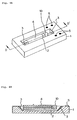
- an optical waveguide of an embodiment of the present invention includes substrate 1 on which V-shaped groove 2 is formed, and a core of optical fiber 4 having a length with which optical fiber 4 can be mounted in V-shaped groove 2 is mounted in V-shaped groove 2.
- Light reflecting films 3 made of a metal having a high reflection factor are formed on inclined surfaces of V-shaped groove 2 which oppose to the end faces at the opposite ends of optical fiber 4.
- the material from which light reflecting films 3 are formed generally includes a thin film of chrome formed on silicon for assuring high adhesion and a thin film of gold formed on the thin chrome film and having a high reflection factor.
- Electrode pads 5 are formed on the surface of substrate 1 at positions around one of light reflecting films 3. The positions and the number of electrode pads 5 may be selected arbitrarily.
- silicon is used as a material of substrate 1.
- substrate 1 The opposite surfaces of substrate 1 are covered with oxide films of SiO 2 , and V-shaped groove 2 is formed by removing SiO 2 at the location at which V-shaped groove 2 is to be formed and performing wet etching substrate 1 with KOH using the remaining SiO 2 as a mask.
- electrode pads 5 are formed as electrode patterns by vapor depositing titanium, platinum and gold in this order on one of the oxide films of SiO 2 .
- another construction wherein a plurality of V-shaped grooves 2 and electrodes are formed on one substrate 1 and optical fiber 4 is mounted in each of V-shaped groove 2 may be employed
- the optical waveguide of the present invention does not have a directivity in regard to the light advancing direction, and accordingly, light may be inputted or outputted to or from any of the left and right sides in Fig. 1B.
- the angle of light reflecting films 3 is 45 degrees and light comes in from the left side and goes out to the right side
- the light is inputted in a direction perpendicular to the surface of substrate 1 from just above the left side one of light reflecting films 3, then the light is reflected by left side light reflecting film 3 and advances in a horizontal direction.
- the reflected light is inputted to optical fiber 4 via the left side end face thereof.
- the light having passed optical fiber 4 goes out from the right side end face of optical fiber 4 and is reflected by the right side one of light reflecting films 3 so that it thereafter goes out to just above right side light reflecting film 3.
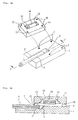
- Fig. 2A and Fig. 2B illustrate a manner in which optical semiconductor device 6 is mounted on the optical waveguide of the present embodiment such that light emitting surface 8 or light receiving surface 9 of optical semiconductor device 6 may be positioned just above light reflecting film 3 at one end of V-shaped groove 2 of the optical waveguide.
- optical semiconductor device 6 is a light emitting element
- another construction wherein optical semiconductor device 6 is a light receiving element is applicable. It is to be noted that, in the latter construction, the light advancing direction is reversed.
- One optical fiber 4 and four electrode pads 5 are disposed on the surface of optical semiconductor device 6, and solder bumps 7 as four electrode pads are disposed on the surface of substrate 1 of the optical waveguide in the proximity of light reflecting film 3 such that they may be registered with the arrangement of electrode pads 5 of optical semiconductor device 6.
- the positions of electrode pads 5 and solder bumps 7 are determined with a high degree of accuracy in advance so that optical semiconductor device 6 may be mounted with the optical axes of electrode pads 5 and solder bumps 7 may be aligned with each other in order that light going out from light emitting surface 8 of optical semiconductor device 6 may be coupled efficiently to the core of optical fiber 4 via light reflecting film 3.
- Optical semiconductor device 6 is joined to substrate 1 of the optical waveguide by solder bumps 7 of gold formed at the electrodes of the surface of substrate 1 of the optical waveguide.
- Optical semiconductor device 6 is temporarily placed on the surface of substrate 1 with the front surface thereof directed downwardly such that solder bumps 7 and electrode pads 5 of optical semiconductor device 6 may contact with each other, and then is entirely heated in a nitrogen atmosphere to melt solder bumps 7 to join optical semiconductor device 6 and substrate 1 to each other. Thereupon, optical semiconductor device 6 is joined with a high degree of mounting accuracy to substrate 1 by the surface tensions of molten solder bumps 7.
- FIG. 2B A manner in which light propagates in the optical waveguide is described with reference to the sectional view of Fig. 2B.
- light emitted from light emitting surface 8 advances downwardly until it is reflected by right side light reflecting film 3 so that it thereafter advances in the leftward direction and propagates in optical fiber 4.
- the light goes out from the left side of optical fiber 4 and is reflected by left side light reflecting film 3 so that it thereafter goes out upwardly.
- Fig. 3A and Fig. 3B illustrate an arrangement of optical waveguides where two optical fibers 4 and 14 of the present embodiment are coupled to each other.
- substrate 1 of one of the optical waveguides is mounted on substrate 11 of the other optical waveguide such that the optical axes of optical fibers 4 and 14 may be aligned with each other with light reflecting films 3 and 13 interposed therebetween.
- Two optical fibers 4 and 14 are coupled to each other while light is bent twice by two light reflecting films 3 and 13. While, in the application shown in Fig. 2B, light is not bent after it is reflected by right side light reflecting film 3, by repeating such a construction as described above, multiple stage connection can be obtained with light reflecting films 3 interposed between them.
- optical fiber 4 or 14 described above can make emergent light therefrom as collimate light if a multi-mode optical fiber having a length equal to an integral number of times one half a wavelength is used for optical fiber 4 or 14, there is an advantage that light reflected by any of light reflecting films 3 advances without being diverged. In this instance, since there is no particular difference in structure except the length of the optical fiber, the application is not shown in the drawings.
- the size of substrate 1 is 4 mm in depth, 4 mm in length and 450 ⁇ m in thickness.
- Substrate 1 is formed by cutting a silicon wafer with a thermally oxidized film of 1 ⁇ m thick added thereto into a piece of a necessary size after the electrode patterns, V-shaped groove 2 and light reflecting films 3 are formed collectively on the silicon wafer.
- the electrode patterns are formed from titanium, platinum or gold, and V-shaped groove 2 are formed by removing the thermally oxidized film on the surface of the wafer with a size of approximately 2 mm in length, 170 ⁇ m in width and 120 ⁇ m in depth using buffered hydrofluoric acid and immersing substrate 1 in potassium hydroxide (KOH) solution to wet etch the silicon.
- KOH potassium hydroxide
- Light reflecting films 3 are formed from chrome of 500 angstrom thick and gold of 2,000 angstrom thick on the inclined surfaces of V-shaped groove 2.
- Optical fiber 4 is formed by cutting a single mode fiber of 1.5 mm long having a diameter of 125 ⁇ m and a core diameter of 10 ⁇ m into a piece of 1.5 mm long and mounted onto and secured to V-shaped groove 2 using an ultraviolet ray setting resin, a thermally setting resin or solder.
- FIG. 2A and Fig. 2B show the application wherein optical semiconductor device 6 is mounted on the optical waveguide of the present invention as described above.
- a PIN photo photodiode of the surface light receiving type is mounted on optical semiconductor device 6.
- the PIN photodiode has light receiving surface 9 of a light receiving diameter of 70 ⁇ m ⁇ disposed at the center of the surface of substrate 1 of indium-phosphorous and has electrodes of a diameter of 70 ⁇ m ⁇ disposed around light receiving surface 9.
- the electrodes serve as lead electrodes of the anodes and the cathodes and pads for solder adhesion upon mounting.
- AuSn solder bumps 7 formed at the electrodes on substrate 1 are heated to a temperature of 300°C so as to be melted to mount the PIN photo photodiode onto substrate 1 at a predetermined position with a high degree of accuracy by an alignment effect by the surface tensions of solder bumps 7.
- the mounting accuracy in the plane obtained is approximately ⁇ 1 ⁇ m and the accuracy in the direction of height obtained is approximately ⁇ 2 ⁇ m.
- the height of solder bumps 7 after adhesion is approximately 50 ⁇ m.
- Fig. 3A and Fig. 3B show the application wherein two optical waveguides of the present embodiment are connected in two stages as described hereinabove.
- V-shaped groove 2 is formed in such a manner as to extend to an end of substrate 1 and light reflecting film 3 is formed only on one inclined surface formed in the proximity of the center of substrate 1.
- This V-shaped groove 2 is suitable to mount therein a cable having an optical connector attached to one end of optical fiber 4 having a pigtail-like shape.
- V-shaped grooves 2 and 12 are formed sufficiently deep so that optical fibers 4 and 14 may not protrude from the surfaces of substrates 1 and 11, respectively. If connection of the waveguides is performed on a straight line, then the angles of the light reflecting films 3 and 13 can be set arbitrarily to establish coupling. When connection of the optical waveguides is performed in a direction displaced from a straight line, the angles of the inclined surfaces of light reflecting films 3 and 13 must be 45 degrees.
- Fig. 4A is a perspective view showing a construction of the second embodiment
- Fig. 4B is a sectional view taken along line D-D' of Fig. 4A.
- Fig. 4A and Fig. 4B show a form wherein lens 10 is disposed between optical fiber 4 and a light reflecting film described hereinabove in connection with the first embodiment. Since this lens 10 converges outgoing light from optical fiber 4 or incoming light to optical fiber 4, light reflected from light reflecting film 3 can advance without being diverged. It is to be noted that, while it is shown in Fig. 4A and Fig. 4B that self focusing lens 10 is disposed only on the right side of optical fiber 4, naturally a better effect can be achieved where it is disposed on the opposite left and right sides of optical fiber 4.
Landscapes
- Physics & Mathematics (AREA)
- General Physics & Mathematics (AREA)
- Optics & Photonics (AREA)
- Optical Couplings Of Light Guides (AREA)
Applications Claiming Priority (2)
| Application Number | Priority Date | Filing Date | Title |
|---|---|---|---|
| JP326610/96 | 1996-12-06 | ||
| JP32661096A JPH10170765A (ja) | 1996-12-06 | 1996-12-06 | 光導波路 |
Publications (2)
| Publication Number | Publication Date |
|---|---|
| EP0846966A2 true EP0846966A2 (de) | 1998-06-10 |
| EP0846966A3 EP0846966A3 (de) | 1998-09-23 |
Family
ID=18189734
Family Applications (1)
| Application Number | Title | Priority Date | Filing Date |
|---|---|---|---|
| EP97121327A Withdrawn EP0846966A3 (de) | 1996-12-06 | 1997-12-04 | Optischer Wellenleiter |
Country Status (2)
| Country | Link |
|---|---|
| EP (1) | EP0846966A3 (de) |
| JP (1) | JPH10170765A (de) |
Cited By (6)
| Publication number | Priority date | Publication date | Assignee | Title |
|---|---|---|---|---|
| WO2002019008A3 (en) * | 2000-08-25 | 2003-08-07 | Hrl Lab Llc | Optical fiber interconnections and a method for fabrication thereof |
| CN100523886C (zh) * | 2007-09-25 | 2009-08-05 | 晶方半导体科技(苏州)有限公司 | 光波导及其制造方法 |
| CN101498813B (zh) * | 2007-09-25 | 2011-01-05 | 苏州晶方半导体科技股份有限公司 | 光波导 |
| CN101498814B (zh) * | 2007-09-25 | 2011-12-28 | 苏州晶方半导体科技股份有限公司 | 光波导 |
| WO2014087122A1 (en) * | 2012-12-04 | 2014-06-12 | University Of Southampton | Apparatus comprising at least one optical device optically coupled to at least one waveguide on an optical chip |
| CN112327417A (zh) * | 2020-11-03 | 2021-02-05 | 中航光电科技股份有限公司 | 一种低损耗多芯阵列光波导连接器 |
Families Citing this family (5)
| Publication number | Priority date | Publication date | Assignee | Title |
|---|---|---|---|---|
| US6670208B2 (en) | 2000-06-23 | 2003-12-30 | Nec Corporation | Optical circuit in which fabrication is easy |
| US6829079B2 (en) | 2000-12-22 | 2004-12-07 | Nec Corporation | Optical path control apparatus with mirror section, and manufacturing method for the same |
| JP2003050329A (ja) * | 2001-08-06 | 2003-02-21 | Toppan Printing Co Ltd | 光・電気配線基板及びその製造方法並びに実装基板 |
| US6944377B2 (en) | 2002-03-15 | 2005-09-13 | Hitachi Maxell, Ltd. | Optical communication device and laminated optical communication module |
| KR101514243B1 (ko) * | 2013-12-27 | 2015-05-04 | 한국광기술원 | 광원장치 |
Family Cites Families (4)
| Publication number | Priority date | Publication date | Assignee | Title |
|---|---|---|---|---|
| CA1211550A (en) * | 1984-03-22 | 1986-09-16 | Northern Telecom Limited | Electronic apparatus with circuit cards and signals optically coupled therebetween |
| DE3543558C2 (de) * | 1985-12-10 | 1996-09-19 | Licentia Gmbh | Opto-elektrische Koppelanordnung |
| US5282080A (en) * | 1991-12-09 | 1994-01-25 | Sdl, Inc. | Surface coupled optical amplifier |
| US5218654A (en) * | 1992-04-16 | 1993-06-08 | Unisys Corporation | Grin rod lens optical backplane bus |
-
1996
- 1996-12-06 JP JP32661096A patent/JPH10170765A/ja active Pending
-
1997
- 1997-12-04 EP EP97121327A patent/EP0846966A3/de not_active Withdrawn
Cited By (12)
| Publication number | Priority date | Publication date | Assignee | Title |
|---|---|---|---|---|
| WO2002019008A3 (en) * | 2000-08-25 | 2003-08-07 | Hrl Lab Llc | Optical fiber interconnections and a method for fabrication thereof |
| US6655853B1 (en) | 2000-08-25 | 2003-12-02 | Hrl Laboratories, Llc | Optical bond-wire interconnections and a method for fabrication thereof |
| US7207728B2 (en) | 2000-08-25 | 2007-04-24 | Hrl Laboratories, Llc | Optical bond-wire interconnections and a method for fabrication thereof |
| CN100523886C (zh) * | 2007-09-25 | 2009-08-05 | 晶方半导体科技(苏州)有限公司 | 光波导及其制造方法 |
| CN101498813B (zh) * | 2007-09-25 | 2011-01-05 | 苏州晶方半导体科技股份有限公司 | 光波导 |
| CN101498814B (zh) * | 2007-09-25 | 2011-12-28 | 苏州晶方半导体科技股份有限公司 | 光波导 |
| WO2014087122A1 (en) * | 2012-12-04 | 2014-06-12 | University Of Southampton | Apparatus comprising at least one optical device optically coupled to at least one waveguide on an optical chip |
| GB2522381A (en) * | 2012-12-04 | 2015-07-22 | Univ Southampton | Apparatus comprising at least one optical device optically coupled to at least one waveguide on an optical chip |
| US9494741B2 (en) | 2012-12-04 | 2016-11-15 | University Of Southampton | Apparatus comprising at least one optical device optically coupled to at least one waveguide on an optical chip |
| GB2522381B (en) * | 2012-12-04 | 2018-06-13 | Univ Southampton | Apparatus comprising at least one optical device optically coupled to at least one waveguide on an optical chip |
| CN112327417A (zh) * | 2020-11-03 | 2021-02-05 | 中航光电科技股份有限公司 | 一种低损耗多芯阵列光波导连接器 |
| CN112327417B (zh) * | 2020-11-03 | 2022-03-15 | 中航光电科技股份有限公司 | 一种低损耗多芯阵列光波导连接器 |
Also Published As
| Publication number | Publication date |
|---|---|
| EP0846966A3 (de) | 1998-09-23 |
| JPH10170765A (ja) | 1998-06-26 |
Similar Documents
| Publication | Publication Date | Title |
|---|---|---|
| US5499309A (en) | Method of fabricating optical component including first and second optical waveguide chips having opposed inclined surfaces | |
| US4750799A (en) | Hybrid optical integrated circuit | |
| EP2413171A1 (de) | Seitlich gekoppelte glasfaserkomponente sowie verarbeitungsverfahren dafür | |
| KR100302144B1 (ko) | 실리콘온인슐레이터 광도파로를 이용한 커넥터형 광트랜시버 | |
| US20030231828A1 (en) | Integrated aspheric optical coupler for RF planarized automatic photonics packaging | |
| JP2700010B2 (ja) | 光電素子パッケージとその形成方法 | |
| JP2924953B2 (ja) | 光素子の実装構造 | |
| US5849204A (en) | Coupling structure for waveguide connection and process for forming the same | |
| KR910005948B1 (ko) | 기판 지지 도파관과 정렬된 콤포넌트를 구비한 소자 | |
| JPH10170765A (ja) | 光導波路 | |
| JP3147564B2 (ja) | 光回路 | |
| JPH0990159A (ja) | 光モジュール及びその組立方法 | |
| US20020131715A1 (en) | Optical coupling | |
| US6361222B1 (en) | Optical device and optical module provided with optical device | |
| JPH09159865A (ja) | 光導波路の接続構造 | |
| JPS6360413A (ja) | 発光素子と光フアイバの結合方法および光導波型結合装置 | |
| JP3256925B2 (ja) | 光導波路装置 | |
| JP2001324647A (ja) | 光ファイバアレイ、光導波路チップ及びこれらを接続した光モジュール | |
| JP2002055264A (ja) | 光学部品をベースに装着した傾斜導波路と整合させる方法および関連する光学装置 | |
| JPH10186183A (ja) | 光アレーモジュール | |
| JP2000009953A (ja) | 波長分波器とこの波長分波器を備えた光送受信モジュール | |
| JP3090335B2 (ja) | 光半導体モジュール | |
| JPH10282370A (ja) | 光モジュール及びその製造方法 | |
| KR100351561B1 (ko) | 수직공동 표면방출 레이저 장치 및 이를 이용한 광송신수단 | |
| JP2755274B2 (ja) | 導波路型受光モジュール |
Legal Events
| Date | Code | Title | Description |
|---|---|---|---|
| PUAI | Public reference made under article 153(3) epc to a published international application that has entered the european phase |
Free format text: ORIGINAL CODE: 0009012 |
|
| AK | Designated contracting states |
Kind code of ref document: A2 Designated state(s): DE FR GB |
|
| AX | Request for extension of the european patent |
Free format text: AL;LT;LV;MK;RO;SI |
|
| PUAL | Search report despatched |
Free format text: ORIGINAL CODE: 0009013 |
|
| AK | Designated contracting states |
Kind code of ref document: A3 Designated state(s): AT BE CH DE DK ES FI FR GB GR IE IT LI LU MC NL PT SE |
|
| AX | Request for extension of the european patent |
Free format text: AL;LT;LV;MK;RO;SI |
|
| 17P | Request for examination filed |
Effective date: 19980812 |
|
| AKX | Designation fees paid |
Free format text: DE FR GB |
|
| RBV | Designated contracting states (corrected) |
Designated state(s): DE FR GB |
|
| 17Q | First examination report despatched |
Effective date: 19991229 |
|
| STAA | Information on the status of an ep patent application or granted ep patent |
Free format text: STATUS: THE APPLICATION IS DEEMED TO BE WITHDRAWN |
|
| 18D | Application deemed to be withdrawn |
Effective date: 20000509 |