EP0375269A2 - Dispositif d'affichage à cristal liquide - Google Patents
Dispositif d'affichage à cristal liquide Download PDFInfo
- Publication number
- EP0375269A2 EP0375269A2 EP89313058A EP89313058A EP0375269A2 EP 0375269 A2 EP0375269 A2 EP 0375269A2 EP 89313058 A EP89313058 A EP 89313058A EP 89313058 A EP89313058 A EP 89313058A EP 0375269 A2 EP0375269 A2 EP 0375269A2
- Authority
- EP
- European Patent Office
- Prior art keywords
- pixels
- light
- light transmission
- liquid crystal
- display unit
- Prior art date
- Legal status (The legal status is an assumption and is not a legal conclusion. Google has not performed a legal analysis and makes no representation as to the accuracy of the status listed.)
- Granted
Links
- 239000004973 liquid crystal related substance Substances 0.000 title claims abstract description 48
- 230000005540 biological transmission Effects 0.000 claims abstract description 76
- 239000000758 substrate Substances 0.000 description 26
- 229910021417 amorphous silicon Inorganic materials 0.000 description 8
- 239000012086 standard solution Substances 0.000 description 6
- 239000004020 conductor Substances 0.000 description 5
- 238000010586 diagram Methods 0.000 description 5
- 239000010408 film Substances 0.000 description 4
- 239000006229 carbon black Substances 0.000 description 3
- 238000005286 illumination Methods 0.000 description 3
- 239000011159 matrix material Substances 0.000 description 3
- 238000010422 painting Methods 0.000 description 3
- 239000004925 Acrylic resin Substances 0.000 description 2
- 229920000178 Acrylic resin Polymers 0.000 description 2
- 239000011521 glass Substances 0.000 description 2
- 230000010287 polarization Effects 0.000 description 2
- 239000011347 resin Substances 0.000 description 2
- 229920005989 resin Polymers 0.000 description 2
- 239000000243 solution Substances 0.000 description 2
- 206010034972 Photosensitivity reaction Diseases 0.000 description 1
- 238000007796 conventional method Methods 0.000 description 1
- 230000003247 decreasing effect Effects 0.000 description 1
- 238000009792 diffusion process Methods 0.000 description 1
- 239000012895 dilution Substances 0.000 description 1
- 238000010790 dilution Methods 0.000 description 1
- 239000006185 dispersion Substances 0.000 description 1
- 238000005530 etching Methods 0.000 description 1
- AMGQUBHHOARCQH-UHFFFAOYSA-N indium;oxotin Chemical compound [In].[Sn]=O AMGQUBHHOARCQH-UHFFFAOYSA-N 0.000 description 1
- 239000003999 initiator Substances 0.000 description 1
- 239000000463 material Substances 0.000 description 1
- 229910052751 metal Inorganic materials 0.000 description 1
- 239000002184 metal Substances 0.000 description 1
- 238000000059 patterning Methods 0.000 description 1
- 229920002120 photoresistant polymer Polymers 0.000 description 1
- 230000036211 photosensitivity Effects 0.000 description 1
- 239000003505 polymerization initiator Substances 0.000 description 1
- 239000010409 thin film Substances 0.000 description 1
Images


Classifications
-
- G—PHYSICS
- G02—OPTICS
- G02F—OPTICAL DEVICES OR ARRANGEMENTS FOR THE CONTROL OF LIGHT BY MODIFICATION OF THE OPTICAL PROPERTIES OF THE MEDIA OF THE ELEMENTS INVOLVED THEREIN; NON-LINEAR OPTICS; FREQUENCY-CHANGING OF LIGHT; OPTICAL LOGIC ELEMENTS; OPTICAL ANALOGUE/DIGITAL CONVERTERS
- G02F1/00—Devices or arrangements for the control of the intensity, colour, phase, polarisation or direction of light arriving from an independent light source, e.g. switching, gating or modulating; Non-linear optics
- G02F1/01—Devices or arrangements for the control of the intensity, colour, phase, polarisation or direction of light arriving from an independent light source, e.g. switching, gating or modulating; Non-linear optics for the control of the intensity, phase, polarisation or colour
- G02F1/13—Devices or arrangements for the control of the intensity, colour, phase, polarisation or direction of light arriving from an independent light source, e.g. switching, gating or modulating; Non-linear optics for the control of the intensity, phase, polarisation or colour based on liquid crystals, e.g. single liquid crystal display cells
- G02F1/133—Constructional arrangements; Operation of liquid crystal cells; Circuit arrangements
- G02F1/1333—Constructional arrangements; Manufacturing methods
- G02F1/1335—Structural association of cells with optical devices, e.g. polarisers or reflectors
- G02F1/133509—Filters, e.g. light shielding masks
-
- G—PHYSICS
- G09—EDUCATION; CRYPTOGRAPHY; DISPLAY; ADVERTISING; SEALS
- G09G—ARRANGEMENTS OR CIRCUITS FOR CONTROL OF INDICATING DEVICES USING STATIC MEANS TO PRESENT VARIABLE INFORMATION
- G09G3/00—Control arrangements or circuits, of interest only in connection with visual indicators other than cathode-ray tubes
- G09G3/20—Control arrangements or circuits, of interest only in connection with visual indicators other than cathode-ray tubes for presentation of an assembly of a number of characters, e.g. a page, by composing the assembly by combination of individual elements arranged in a matrix no fixed position being assigned to or needed to be assigned to the individual characters or partial characters
- G09G3/34—Control arrangements or circuits, of interest only in connection with visual indicators other than cathode-ray tubes for presentation of an assembly of a number of characters, e.g. a page, by composing the assembly by combination of individual elements arranged in a matrix no fixed position being assigned to or needed to be assigned to the individual characters or partial characters by control of light from an independent source
- G09G3/36—Control arrangements or circuits, of interest only in connection with visual indicators other than cathode-ray tubes for presentation of an assembly of a number of characters, e.g. a page, by composing the assembly by combination of individual elements arranged in a matrix no fixed position being assigned to or needed to be assigned to the individual characters or partial characters by control of light from an independent source using liquid crystals
- G09G3/3607—Control arrangements or circuits, of interest only in connection with visual indicators other than cathode-ray tubes for presentation of an assembly of a number of characters, e.g. a page, by composing the assembly by combination of individual elements arranged in a matrix no fixed position being assigned to or needed to be assigned to the individual characters or partial characters by control of light from an independent source using liquid crystals for displaying colours or for displaying grey scales with a specific pixel layout, e.g. using sub-pixels
-
- G—PHYSICS
- G02—OPTICS
- G02F—OPTICAL DEVICES OR ARRANGEMENTS FOR THE CONTROL OF LIGHT BY MODIFICATION OF THE OPTICAL PROPERTIES OF THE MEDIA OF THE ELEMENTS INVOLVED THEREIN; NON-LINEAR OPTICS; FREQUENCY-CHANGING OF LIGHT; OPTICAL LOGIC ELEMENTS; OPTICAL ANALOGUE/DIGITAL CONVERTERS
- G02F1/00—Devices or arrangements for the control of the intensity, colour, phase, polarisation or direction of light arriving from an independent light source, e.g. switching, gating or modulating; Non-linear optics
- G02F1/01—Devices or arrangements for the control of the intensity, colour, phase, polarisation or direction of light arriving from an independent light source, e.g. switching, gating or modulating; Non-linear optics for the control of the intensity, phase, polarisation or colour
- G02F1/13—Devices or arrangements for the control of the intensity, colour, phase, polarisation or direction of light arriving from an independent light source, e.g. switching, gating or modulating; Non-linear optics for the control of the intensity, phase, polarisation or colour based on liquid crystals, e.g. single liquid crystal display cells
- G02F1/133—Constructional arrangements; Operation of liquid crystal cells; Circuit arrangements
- G02F1/1333—Constructional arrangements; Manufacturing methods
- G02F1/1343—Electrodes
- G02F1/134309—Electrodes characterised by their geometrical arrangement
- G02F1/134345—Subdivided pixels, e.g. for grey scale or redundancy
-
- G—PHYSICS
- G02—OPTICS
- G02F—OPTICAL DEVICES OR ARRANGEMENTS FOR THE CONTROL OF LIGHT BY MODIFICATION OF THE OPTICAL PROPERTIES OF THE MEDIA OF THE ELEMENTS INVOLVED THEREIN; NON-LINEAR OPTICS; FREQUENCY-CHANGING OF LIGHT; OPTICAL LOGIC ELEMENTS; OPTICAL ANALOGUE/DIGITAL CONVERTERS
- G02F1/00—Devices or arrangements for the control of the intensity, colour, phase, polarisation or direction of light arriving from an independent light source, e.g. switching, gating or modulating; Non-linear optics
- G02F1/01—Devices or arrangements for the control of the intensity, colour, phase, polarisation or direction of light arriving from an independent light source, e.g. switching, gating or modulating; Non-linear optics for the control of the intensity, phase, polarisation or colour
- G02F1/13—Devices or arrangements for the control of the intensity, colour, phase, polarisation or direction of light arriving from an independent light source, e.g. switching, gating or modulating; Non-linear optics for the control of the intensity, phase, polarisation or colour based on liquid crystals, e.g. single liquid crystal display cells
- G02F1/133—Constructional arrangements; Operation of liquid crystal cells; Circuit arrangements
- G02F1/136—Liquid crystal cells structurally associated with a semi-conducting layer or substrate, e.g. cells forming part of an integrated circuit
- G02F1/1362—Active matrix addressed cells
- G02F1/13624—Active matrix addressed cells having more than one switching element per pixel
-
- G—PHYSICS
- G02—OPTICS
- G02F—OPTICAL DEVICES OR ARRANGEMENTS FOR THE CONTROL OF LIGHT BY MODIFICATION OF THE OPTICAL PROPERTIES OF THE MEDIA OF THE ELEMENTS INVOLVED THEREIN; NON-LINEAR OPTICS; FREQUENCY-CHANGING OF LIGHT; OPTICAL LOGIC ELEMENTS; OPTICAL ANALOGUE/DIGITAL CONVERTERS
- G02F2203/00—Function characteristic
- G02F2203/30—Gray scale
-
- G—PHYSICS
- G09—EDUCATION; CRYPTOGRAPHY; DISPLAY; ADVERTISING; SEALS
- G09G—ARRANGEMENTS OR CIRCUITS FOR CONTROL OF INDICATING DEVICES USING STATIC MEANS TO PRESENT VARIABLE INFORMATION
- G09G2300/00—Aspects of the constitution of display devices
- G09G2300/04—Structural and physical details of display devices
- G09G2300/0439—Pixel structures
- G09G2300/0443—Pixel structures with several sub-pixels for the same colour in a pixel, not specifically used to display gradations
-
- G—PHYSICS
- G09—EDUCATION; CRYPTOGRAPHY; DISPLAY; ADVERTISING; SEALS
- G09G—ARRANGEMENTS OR CIRCUITS FOR CONTROL OF INDICATING DEVICES USING STATIC MEANS TO PRESENT VARIABLE INFORMATION
- G09G3/00—Control arrangements or circuits, of interest only in connection with visual indicators other than cathode-ray tubes
- G09G3/20—Control arrangements or circuits, of interest only in connection with visual indicators other than cathode-ray tubes for presentation of an assembly of a number of characters, e.g. a page, by composing the assembly by combination of individual elements arranged in a matrix no fixed position being assigned to or needed to be assigned to the individual characters or partial characters
- G09G3/2007—Display of intermediate tones
- G09G3/2074—Display of intermediate tones using sub-pixels
Definitions
- the present invention relates to a liquid crystal device allowing multi-gradation display.
- a liquid crystal display device including a plurality of display units is disclosed in Japanese Published Unexamined Patent Application (PUPA) No. 58-220185.
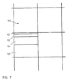
- each display unit 100 is constituted by four pixels (picture elements) 101, 102, 104, 108, (see Figure 7 of the drawings accompanying this Specification) with area ratios of 1 : 2 : 4 : 8, allowing a 16-gradation (gray scale) display by the selection and non-selection of different ones of the four pixels.
- the largest pixel 108 has an area eight times that of the smallest pixel 101. There is a limit for decreasing the area of a display unit, and the arrangement described cannot, therefore, be applied to a liquid crystal display device having high resolution and a large area.
- the light transmission factor of a liquid crystal used in a display device varies when a voltage applied to the liquid crystal is varied, it is considered theoretically possible to obtain a required gradation by varying the voltage applied to the liquid crystal.
- the object of the present invention is to provide an improved liquid crystal display device.
- the present invention relates to a liquid crystal display device comprising a plurality of display units each having n (where n is a positive integer) pixels (picture elements), each of which pixels can be made either to transmit or to receive light, means for applying a voltage to the region of the liquid crystal adjacent to each pixel in order to control the transmission characteristic of each pixel and a light transmission factor control layer for controlling the light transmission factor of each pixel.
- the display device is characterised in that the ratios between the light transmission factors of the pixels in each display unit are 20 : 21 : 22 ... 2 n-1 .
- each display unit can exhibit a selected one of 2 n different gradations of light transmission.
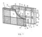
- Fig. 1 shows a liquid crystal display device according to the present invention which provides 16 gradations in the light transmission factor of each display unit of the display device.
- the display device includes a plurality of display units DU and each display unit DU is composed of a set of four pixels (picture elements) T1, T2, T3, and T4 located so as to form a square (see also Fig. 2).
- the portions of the display device corresponding to the sets of pixels T1, T2, T3, and T4 in Fig. 2 are located on a transparent glass substrate 2, which is called the TFT array substrate.
- the substrate 2 is provided with sets of transparent pixel electrodes 11, 12, 13, and 14 made of indium tin oxide (hereinafter called ITO), one set of electrodes for each pixel.
- ITO indium tin oxide
- Each set of pixel electrodes 11, 12, 13, and 14 is connected to a source electrode 20 of a respective one of a plurality of thin-film transistors (hereinafter called a-Si TFT) 16 made of amorphous silicon, each of which controls the application of a voltage to a liquid crystal in the corresponding pixel.
- a-Si TFT thin-film transistors
- Each a-Si TFT 16 is connected at its gate electrode (not shown) to an address conductor 22, and at its drain electrode 18 to a data conductor 23. Also, a liquid crystal orientation film (not shown) is provided extending over the whole of the substrate 2 inside the pixel electrodes 12.
- sets of light transmission factor control layers 31, 32, 33, and 34 are provided, one for each pixel.
- the light transmission factor control layers 31, 32, 33, and 34 of each set are disposed in the regions of the corresponding pixels T1, T2, T3, and T4, respectively, and the ratios between the light transmission factors of the layers in each set are 20 : 21 : 22 : 23, that is, 1 : 2 : 4 : 8.
- a common electrode 36 is provided all over the whole area of the counter substrate 4. Inside the common electrode 36 a liquid crystal orientation film (not shown) is provided over the whole area of the substrate 4. A liquid crystal 3 is located between the TFT array substrate 2 and the counter substrate 4, or, more correctly, between an orientation film extending over the sets of pixel electrodes 11, 12, 13, and 14 and an orientation film extending over the common electrode 36.
- a back illumination source 46 At the rear of the TFT array substrate 2 (as viewed in Fig. 1) is provided a back illumination source 46, and outside the TFT array substrate 2 (that is, on the side facing towards the back illumination source 46) is provided a polarizing plate 40. Between the back illumination source 46 and the polarizing plate 40 is a diffusion plate 44 for diffusing light. Also, outside the counter electrode 4 (that is, on the opposite side from the TFT array substrate 2) is provided a polarizing plate 42.
- the a-Si TFT 16 which is located on both these conductors is placed in the ON state and a voltage is applied to the corresponding portion of the liquid crystal 3.
- the directions of polarization of the polarizing plates 40 and 42 of the liquid crystal display device in Fig. 1 are perpendicular to each other and the molecular axis of the liquid crystal, as between the portions nearest to the substrate 2 and to the substrate 4 respectively, is twisted by 90_ when no voltage has been applied to the liquid crystal 3, then, when no voltage is applied to a region of the liquid crystal, this region of the liquid crystal allows light to pass through it.
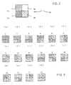
- the application of voltages to the pixels T1, T2, T3, and T4 and the corresponding light transmission and light interception can be independently controlled by the a-Si TFT's 16. Accordingly, sixteen different combinations of light transmission and light interception in the pixels T1, T2, T3, and T4 are available, as shown in Fig. 3, bearing in mind that the light transmission factors of the pixels are in the ratios 1 : 2 : 4 : 8.
- Fig. 3(a) shows a state in which all of the pixels T1, T2, T3, and T4 of a display unit DU intercept light.
- the amount of light transmission of the whole display unit DU in this case is as follows, as a relative value:
- Fig. 3(b) shows a state in which the pixel T1 allows light to pass through it, and the pixels T2, T3, and T4 intercept light.
- the amount of light transmission of the whole display unit DU in this case is as follows, as a relative value:
- Fig. 3(c) shows a state in which the pixel T2 allows light to pass through it and the pixels T1, T3, and T4 intercept light.
- the amount of light transmission of the whole display unit DU in this case is as follows, as a relative value:
- Fig. 3(d) shows a state in which the pixel T3 allows light to pass through it and the pixels T1, T2, and T4 intercept light.
- An amount of light transmission of the whole display unit DU in this case is as follows, as a relative value:
- Fig. 3(e) shows a state in which the pixel T4 allows light to pass through it and the pixels T1, T2, and T3 intercept light.
- the amount of light transmission of the whole display unit DU in this case is as follows, as a relative value:
- Fig. 3(f) shows a state in which the pixels T1 and T2 allow light to pass through them and the pixels T3 and T4 intercept light.
- the amount of light transmission of the whole display unit DU in this case is as follows, as a relative value:
- Fig. 3(g) shows a state in which the pixels T2 and T3 allow light to pass through them and the pixels T1 and T4 intercept light.
- the amount of light transmission of the whole display unit DU in this case is as follows, as a relative value:
- Fig. 3(h) shows a state in which the pixels T3 and T4 allow light to pass through them and the pixels T1 and T2 intercept light.
- the amount of light transmission of the whole display unit DU in this case is as follows, as a relative value:
- Fig. 3(i) shows a state in which the pixels T1 and T3 allow light to pass through them and the pixels T2 and T4 intercept light.
- the amount of light transmission of the whole display unit DU in this case is as follows, as a relative value:
- Fig 3(j) shows a state in which the pixels T2 and T4 allow light to pass through them and the pixels T1 and T3 intercept light.
- the amount of light transmission of the whole display unit DU in this case is as follows, as a relative value:
- Fig. 3(k) shows a state in which the pixels T1 and T4 allow light to pass through them and the pixels T2 and T3 intercept light.
- the amount of light transmission of the whole display unit DU in this case is as follows, as a relative value:
- Fig. 3(l) shows a state in which the pixels T2, T3, and T4 allow light to pass through them and the pixel T1 intercepts light.
- the amount of light transmission of the whole display unit DU in this case is as follows, as a relative value:
- Fig. 3(m) shows a state in which the pixels T1, T3, and T4 allow light to pass through them and the pixel T2 intercepts light.
- the amount of light transmission of the whole display unit DU in this case is as follows, as a relative value:
- Fig. 3(n) shows a state in which the pixels T1, T2, and T4 allow light to pass through them and the pixel T3 intercepts light.
- the amount of light transmission of the whole display unit DU in this case is as follows, as a relative value:
- Fig. 3(o) shows a state in which the pixels T1, T2, and T3 allow light to pass through them and the pixel T4 intercepts light.
- the amount of light transmission of the whole display unit DU in this case is as follows, as a relative value:
- Fig. 3(p) shows a state in which all the pixels T1, T2, T3, and T4 allow light to pass through them.
- the amount of light transmission of the whole display unit DU in this case is as follows, as a relative value:
- the ratios of the light transmission factors of the pixels T1, T2, T3, and T4 are arranged to be 1 : 2 : 4 : 8, different combinations of the light transmission and interception of the pixels T1, T2, T3, and T4 allow relative amounts of light transmissions of 0/15, 1/15, 2/15, 3/15, 4/15, 5/15, 6/15, 7/15, 8/15, 9/15, 10/15, 11/15, 12/15, 13/15, 14/15, and 15/15 to be obtained, which allows 16 gradations to be attained.
- the light transmission factors of the light transmission factor control layers 31, 32, 33, and 34 need only to be, for example, 12.5%, 25.0%, 50.0%, and 100%. This can be realized, for example, by controlling the amount of dispersion of carbon black into an acrylic resin which is used to form each control layer.
- a standard solution (hereinafter called a STD solution), produced by adding a photopolymerization initiator and carbon black to acrylic resin and performing viscosity adjustment and dilution thereof, is rotatively applied with painting at speeds of 520 RPM and 900 RPM, allowing the light transmission factors of 12.5% and 25.0% respectively to be obtained.
- the STD solution is diluted in such a manner that the carbon black component amounting to 30% and is rotated at a speed of 650 RPM, a light transmission factor of 50.0% can be obtained.
- Fig. 4 shows the relationship between the revolutions per minute (RPM) and the light transmission factor (%) of a control layer in the case where a required light transmission factor is obtained by rotative painting using either a standard solution (STD) or a diluted standard solution (STDDIL).
- RPM revolutions per minute
- STDDIL diluted standard solution
- Fig. 5 shows an example of an arrangement of pixels in the case where a display unit DU is composed of three adjacent pixels.
- Three square-shaped pixels S1, S2, and S3 are located respectively at the apexes of an inverted regular triangle to form a single display unit, and the ratios of the light transmission factors of the pixels are: 20 : 21 : 22 that is, 1 : 2 : 4.
- Fig. 6(a) shows a state in which all of the pixels S1, S2, and S3 intercept light.
- the amount of light transmission of the display unit DU in this case is as follows, as a relative value:
- Fig. 6(b) shows a state in which the pixel S1 allows light to pass through it and the pixels S2 and S3 intercept light.
- the amount of light transmission of the display unit DU in this case is as follows, as a relative value:
- Fig. 6(c) shows a state in which the pixel S2 allows light to pass through it and the pixels S1 and S3 intercept light.
- the amount of light transmission of the display unit DU in this case is as follows, as a relative value:
- Fig. 6(d) shows a state in which the pixel S3 alloms light to pass through it and the pixels S1 and S2 intercept light.
- the amount of light transmission of the display unit DU in this case is as follows, as a relative value:
- Fig. 6(e) shows a state in which the pixels S1 and S2 allow light to pass through them and the pixel S3 intercepts light.
- the amount of light transmission of the display unit DU in this case is as follows, as a relative value:
- Fig. 6(f) shows a state in which the pixels S1 and S3 allow light to pass through them and the pixel S2 intercepts light.
- the amount of light transmission of the display unit DU in this case is as follows, as a relative value:
- Fig. 6(g) shows a state in which the pixels S2 and S3 allow light to pass through them and the pixel S1 intercepts light.
- the amount of light transmission of the display unit DU in this case is as follows, as a relative value:
- Fig. 6(h) shows a state in which all the pixels S1, S2, and S3 allow light to pass through them.
- the amount of light transmission of the display unit DU in this case is as follows, as a relative value:
- the combinations of the light transmission and interception of the three pixels allows relative amounts of the light transmission of 0/7, 1/7, 2/7, 3/7, 4/7, 5/7, 6/7 and 7/7 to be obtained, which allows eight gradations to be attained.
- the above-mentioned embodiments are those in the cases where one display unit DU is formed from either four or three pixels.
- TFT is employed as a switching element which controls the application of voltages to liquid crystals in a pixel domain
- present invention is not limited by this.
- MIM metal-insulator-metal
- the present invention can be applied not only to the above-mentioned so-called active matrix type liquid crystal, but also to a simple matrix type liquid crystal.
- a simple matrix type the application of voltages to pixels in the region of a liquid crystal where an X electrode and a Y electrode intersect is selected to control light transmission and interception for the liquid crystal in the pixel region concerned.
- a light transmission factor control layer is provided on the side of the counter electrode 4. It may alternatively be provided on the pixel electrodes on the substrate on the side of the switching elements such as TFT.
- the present invention allows a multi-gradation display without the necessity of enlarging an area in one display unit, or of finely adjusting voltages applied to the liquid crystals in each pixel.
Landscapes
- Physics & Mathematics (AREA)
- Chemical & Material Sciences (AREA)
- Crystallography & Structural Chemistry (AREA)
- Engineering & Computer Science (AREA)
- Nonlinear Science (AREA)
- General Physics & Mathematics (AREA)
- Theoretical Computer Science (AREA)
- Mathematical Physics (AREA)
- Computer Hardware Design (AREA)
- Optics & Photonics (AREA)
- Liquid Crystal (AREA)
- Devices For Indicating Variable Information By Combining Individual Elements (AREA)
- Liquid Crystal Display Device Control (AREA)
Applications Claiming Priority (2)
| Application Number | Priority Date | Filing Date | Title |
|---|---|---|---|
| JP320564/88 | 1988-12-21 | ||
| JP63320564A JPH02166419A (ja) | 1988-12-21 | 1988-12-21 | 液晶表示装置 |
Publications (3)
| Publication Number | Publication Date |
|---|---|
| EP0375269A2 true EP0375269A2 (fr) | 1990-06-27 |
| EP0375269A3 EP0375269A3 (en) | 1990-09-12 |
| EP0375269B1 EP0375269B1 (fr) | 1994-05-18 |
Family
ID=18122841
Family Applications (1)
| Application Number | Title | Priority Date | Filing Date |
|---|---|---|---|
| EP89313058A Expired - Lifetime EP0375269B1 (fr) | 1988-12-21 | 1989-12-13 | Dispositif d'affichage à cristal liquide |
Country Status (5)
| Country | Link |
|---|---|
| US (1) | US5121235A (fr) |
| EP (1) | EP0375269B1 (fr) |
| JP (1) | JPH02166419A (fr) |
| CA (1) | CA2006244C (fr) |
| DE (1) | DE68915414T2 (fr) |
Cited By (3)
| Publication number | Priority date | Publication date | Assignee | Title |
|---|---|---|---|---|
| WO2001073737A1 (fr) | 2000-03-30 | 2001-10-04 | Seiko Epson Corporation | Affichage |
| EP1251480A3 (fr) * | 2001-04-19 | 2004-01-02 | Spectratech Inc. | Affichage monochrome pixellisé avec echelle de gradations ameliorée par utilisation de sous-pixels avec filtres à densité neutre ayant une échelle binaire |
| US6801180B2 (en) | 2000-03-30 | 2004-10-05 | Seiko Epson Corporation | Display device |
Families Citing this family (11)
| Publication number | Priority date | Publication date | Assignee | Title |
|---|---|---|---|---|
| TW228633B (fr) * | 1991-01-17 | 1994-08-21 | Semiconductor Energy Res Co Ltd | |
| KR940009449B1 (ko) * | 1991-04-06 | 1994-10-13 | 주식회사금성사 | 칼라비디오 프린터의 노광장치 |
| US5656526A (en) * | 1993-12-07 | 1997-08-12 | Kabushiki Kaisha Toshiba | Method of fabricating a display device |
| GB2286058A (en) * | 1994-01-21 | 1995-08-02 | Sharp Kk | Switchable holographic apparatus |
| US5606437A (en) * | 1995-03-31 | 1997-02-25 | Rockwell International | Direct drive split pixel structure for active matrix liquid crystal displays |
| JP3075134B2 (ja) * | 1995-04-04 | 2000-08-07 | 株式会社日立製作所 | 反射型液晶表示装置 |
| JPH1068931A (ja) * | 1996-08-28 | 1998-03-10 | Sharp Corp | アクティブマトリクス型液晶表示装置 |
| JP2001242828A (ja) | 2000-02-25 | 2001-09-07 | Internatl Business Mach Corp <Ibm> | 多階調表現のための画像表示装置、液晶表示装置、および画像表示方法 |
| JP2002297085A (ja) * | 2001-03-30 | 2002-10-09 | Ricoh Co Ltd | 階調表示方法及び階調表示装置 |
| US20050007327A1 (en) * | 2002-04-22 | 2005-01-13 | Cliff Elion | Color image display apparatus |
| CN100443974C (zh) * | 2005-09-30 | 2008-12-17 | 群康科技(深圳)有限公司 | 液晶显示模组 |
Family Cites Families (19)
| Publication number | Priority date | Publication date | Assignee | Title |
|---|---|---|---|---|
| US3626241A (en) * | 1969-12-24 | 1971-12-07 | Bell Telephone Labor Inc | Gray scale gaseous display |
| JPS5276897A (en) * | 1975-12-23 | 1977-06-28 | Hitachi Ltd | Half tone picture display device using liquid crystal matrix panel |
| US4495492A (en) * | 1982-05-05 | 1985-01-22 | Litton Systems, Inc. | Magneto-optic chip with gray-scale capability |
| JPS58220185A (ja) * | 1982-06-17 | 1983-12-21 | セイコーインスツルメンツ株式会社 | 表示素子 |
| US4486785A (en) * | 1982-09-30 | 1984-12-04 | International Business Machines Corporation | Enhancement of video images by selective introduction of gray-scale pels |
| JPS5961818A (ja) * | 1982-10-01 | 1984-04-09 | Seiko Epson Corp | 液晶表示装置 |
| CH666560A5 (de) * | 1983-03-01 | 1988-07-29 | Tadeusz Bobak | Anzeigevorrichtung. |
| US4531160A (en) * | 1983-05-03 | 1985-07-23 | Itek Corporation | Display processor system and method |
| JPS60188924A (ja) * | 1984-03-09 | 1985-09-26 | Citizen Watch Co Ltd | 表示装置 |
| JPS60172131U (ja) * | 1984-04-20 | 1985-11-14 | ホシデン株式会社 | カラ−液晶表示器 |
| US4712877A (en) * | 1985-01-18 | 1987-12-15 | Canon Kabushiki Kaisha | Ferroelectric display panel of varying thickness and driving method therefor |
| JP2505756B2 (ja) * | 1986-07-22 | 1996-06-12 | キヤノン株式会社 | 光学変調素子の駆動法 |
| GB2198869B (en) * | 1986-12-19 | 1990-08-15 | Philips Electronic Associated | Matrix display devices |
| JPS63241528A (ja) * | 1987-03-28 | 1988-10-06 | Nippon Telegr & Teleph Corp <Ntt> | 光論理演算の方法及びその装置 |
| US4840460A (en) * | 1987-11-13 | 1989-06-20 | Honeywell Inc. | Apparatus and method for providing a gray scale capability in a liquid crystal display unit |
| US4892391A (en) * | 1988-02-16 | 1990-01-09 | General Electric Company | Method of arranging the cells within the pixels of a color alpha-numeric display device |
| JPH01214898A (ja) * | 1988-02-24 | 1989-08-29 | Ricoh Co Ltd | 多階調表示方式 |
| JPH0227316A (ja) * | 1988-07-15 | 1990-01-30 | Fujitsu Ltd | 液晶表示装置 |
| US4921334A (en) * | 1988-07-18 | 1990-05-01 | General Electric Company | Matrix liquid crystal display with extended gray scale |
-
1988
- 1988-12-21 JP JP63320564A patent/JPH02166419A/ja active Pending
-
1989
- 1989-12-13 EP EP89313058A patent/EP0375269B1/fr not_active Expired - Lifetime
- 1989-12-13 DE DE68915414T patent/DE68915414T2/de not_active Expired - Fee Related
- 1989-12-20 CA CA002006244A patent/CA2006244C/fr not_active Expired - Fee Related
- 1989-12-21 US US07/454,333 patent/US5121235A/en not_active Expired - Fee Related
Cited By (4)
| Publication number | Priority date | Publication date | Assignee | Title |
|---|---|---|---|---|
| WO2001073737A1 (fr) | 2000-03-30 | 2001-10-04 | Seiko Epson Corporation | Affichage |
| US6801180B2 (en) | 2000-03-30 | 2004-10-05 | Seiko Epson Corporation | Display device |
| EP1251480A3 (fr) * | 2001-04-19 | 2004-01-02 | Spectratech Inc. | Affichage monochrome pixellisé avec echelle de gradations ameliorée par utilisation de sous-pixels avec filtres à densité neutre ayant une échelle binaire |
| US6961040B2 (en) | 2001-04-19 | 2005-11-01 | Eizo Nanao Corporation | Two-dimensional monochrome bit face display |
Also Published As
| Publication number | Publication date |
|---|---|
| DE68915414D1 (de) | 1994-06-23 |
| DE68915414T2 (de) | 1994-11-24 |
| EP0375269A3 (en) | 1990-09-12 |
| EP0375269B1 (fr) | 1994-05-18 |
| US5121235A (en) | 1992-06-09 |
| CA2006244C (fr) | 1993-08-31 |
| CA2006244A1 (fr) | 1990-06-21 |
| JPH02166419A (ja) | 1990-06-27 |
Similar Documents
| Publication | Publication Date | Title |
|---|---|---|
| EP0375269B1 (fr) | Dispositif d'affichage à cristal liquide | |
| EP0316708B1 (fr) | Appareil pour munir d'une faculté de reproduction d'une échelle de gris un dispositif d'affichage à cristal liquide | |
| US8681303B2 (en) | Liquid crystal display device comprising periodically changed permutations of at least two types of electrode-pattern pairs | |
| US7145580B2 (en) | Gray scale voltage generator, method of generating gray scale voltage and transmissive and reflective type liquid crystal display device using the same | |
| US5790215A (en) | Liquid crystal display device | |
| KR101383706B1 (ko) | 액정 표시 장치 및 그의 구동 방법 | |
| EP0685756A2 (fr) | Afficheur à cristal liquide comportant une pluralité de sous-pixels | |
| US20090146936A1 (en) | Liquid crystal display and method of manufacturing the same | |
| KR0149296B1 (ko) | 광 시야각 구동회로와 그 구동방법 | |
| US8797252B2 (en) | Liquid crystal display apparatus and method for generating a driver signal based on resistance ratios | |
| KR20030058762A (ko) | 액정 패널의 구동장치 및 그 구동방법 | |
| KR100593490B1 (ko) | 액정표시장치 | |
| US20210407447A1 (en) | Pixel circuit and liquid crystal display panel | |
| CN116736591B (zh) | 阵列基板及显示面板、显示装置 | |
| EP0478043B1 (fr) | Ecran de visualisation | |
| US5446567A (en) | Liquid crystal display with first and second aperatures where one aperature has protuberances | |
| US6753938B2 (en) | Liquid crystal display device using both reflection and transmission | |
| KR100326880B1 (ko) | 액정표시소자 | |
| CN108269504B (zh) | 像素排布结构、像素驱动电路及显示装置 | |
| US5748268A (en) | Quasi-tiled active matrix display | |
| CN110262113B (zh) | 显示装置 | |
| EP0464898A2 (fr) | Dispositif optique de traitement de données | |
| JP4712215B2 (ja) | 液晶表示装置ならびにそれを備える携帯電話機および携帯情報端末機器 | |
| KR100430798B1 (ko) | 액정표시장치용박막트랜지스터기판 | |
| KR20040085678A (ko) | 4색 액정 표시 장치와 구동 방법 |
Legal Events
| Date | Code | Title | Description |
|---|---|---|---|
| PUAI | Public reference made under article 153(3) epc to a published international application that has entered the european phase |
Free format text: ORIGINAL CODE: 0009012 |
|
| AK | Designated contracting states |
Kind code of ref document: A2 Designated state(s): DE FR GB IT |
|
| PUAL | Search report despatched |
Free format text: ORIGINAL CODE: 0009013 |
|
| AK | Designated contracting states |
Kind code of ref document: A3 Designated state(s): DE FR GB IT |
|
| 17P | Request for examination filed |
Effective date: 19901025 |
|
| 17Q | First examination report despatched |
Effective date: 19921109 |
|
| GRAA | (expected) grant |
Free format text: ORIGINAL CODE: 0009210 |
|
| AK | Designated contracting states |
Kind code of ref document: B1 Designated state(s): DE FR GB IT |
|
| REF | Corresponds to: |
Ref document number: 68915414 Country of ref document: DE Date of ref document: 19940623 |
|
| ITF | It: translation for a ep patent filed | ||
| ET | Fr: translation filed | ||
| PLBE | No opposition filed within time limit |
Free format text: ORIGINAL CODE: 0009261 |
|
| STAA | Information on the status of an ep patent application or granted ep patent |
Free format text: STATUS: NO OPPOSITION FILED WITHIN TIME LIMIT |
|
| 26N | No opposition filed | ||
| PGFP | Annual fee paid to national office [announced via postgrant information from national office to epo] |
Ref country code: GB Payment date: 19951127 Year of fee payment: 7 |
|
| PGFP | Annual fee paid to national office [announced via postgrant information from national office to epo] |
Ref country code: FR Payment date: 19951128 Year of fee payment: 7 |
|
| PGFP | Annual fee paid to national office [announced via postgrant information from national office to epo] |
Ref country code: DE Payment date: 19951229 Year of fee payment: 7 |
|
| PG25 | Lapsed in a contracting state [announced via postgrant information from national office to epo] |
Ref country code: GB Effective date: 19961213 |
|
| GBPC | Gb: european patent ceased through non-payment of renewal fee |
Effective date: 19961213 |
|
| PG25 | Lapsed in a contracting state [announced via postgrant information from national office to epo] |
Ref country code: FR Effective date: 19970829 |
|
| PG25 | Lapsed in a contracting state [announced via postgrant information from national office to epo] |
Ref country code: DE Effective date: 19970902 |
|
| REG | Reference to a national code |
Ref country code: FR Ref legal event code: ST |
|
| PG25 | Lapsed in a contracting state [announced via postgrant information from national office to epo] |
Ref country code: IT Free format text: LAPSE BECAUSE OF NON-PAYMENT OF DUE FEES;WARNING: LAPSES OF ITALIAN PATENTS WITH EFFECTIVE DATE BEFORE 2007 MAY HAVE OCCURRED AT ANY TIME BEFORE 2007. THE CORRECT EFFECTIVE DATE MAY BE DIFFERENT FROM THE ONE RECORDED. Effective date: 20051213 |