EP0478043B1 - Ecran de visualisation - Google Patents
Ecran de visualisation Download PDFInfo
- Publication number
- EP0478043B1 EP0478043B1 EP91202313A EP91202313A EP0478043B1 EP 0478043 B1 EP0478043 B1 EP 0478043B1 EP 91202313 A EP91202313 A EP 91202313A EP 91202313 A EP91202313 A EP 91202313A EP 0478043 B1 EP0478043 B1 EP 0478043B1
- Authority
- EP
- European Patent Office
- Prior art keywords
- sub
- pixels
- pixel
- display device
- adjustable
- Prior art date
- Legal status (The legal status is an assumption and is not a legal conclusion. Google has not performed a legal analysis and makes no representation as to the accuracy of the status listed.)
- Expired - Lifetime
Links
- 230000005540 biological transmission Effects 0.000 claims description 26
- 239000007788 liquid Substances 0.000 claims description 3
- 239000011159 matrix material Substances 0.000 claims description 2
- 239000000758 substrate Substances 0.000 description 7
- 239000004973 liquid crystal related substance Substances 0.000 description 5
- 239000000463 material Substances 0.000 description 5
- 239000005262 ferroelectric liquid crystals (FLCs) Substances 0.000 description 3
- 239000004988 Nematic liquid crystal Substances 0.000 description 2
- 230000001419 dependent effect Effects 0.000 description 2
- 238000011282 treatment Methods 0.000 description 2
- 239000004020 conductor Substances 0.000 description 1
- 239000013078 crystal Substances 0.000 description 1
- 239000002178 crystalline material Substances 0.000 description 1
- 238000010586 diagram Methods 0.000 description 1
- 230000000694 effects Effects 0.000 description 1
- 239000011521 glass Substances 0.000 description 1
- 230000005484 gravity Effects 0.000 description 1
- 238000005286 illumination Methods 0.000 description 1
- AMGQUBHHOARCQH-UHFFFAOYSA-N indium;oxotin Chemical compound [In].[Sn]=O AMGQUBHHOARCQH-UHFFFAOYSA-N 0.000 description 1
- 229910052751 metal Inorganic materials 0.000 description 1
- 239000002184 metal Substances 0.000 description 1
- 230000003287 optical effect Effects 0.000 description 1
- 230000003071 parasitic effect Effects 0.000 description 1
- 239000010453 quartz Substances 0.000 description 1
- 238000007789 sealing Methods 0.000 description 1
- VYPSYNLAJGMNEJ-UHFFFAOYSA-N silicon dioxide Inorganic materials O=[Si]=O VYPSYNLAJGMNEJ-UHFFFAOYSA-N 0.000 description 1
- 230000007704 transition Effects 0.000 description 1
Images
Classifications
-
- G—PHYSICS
- G09—EDUCATION; CRYPTOGRAPHY; DISPLAY; ADVERTISING; SEALS
- G09G—ARRANGEMENTS OR CIRCUITS FOR CONTROL OF INDICATING DEVICES USING STATIC MEANS TO PRESENT VARIABLE INFORMATION
- G09G3/00—Control arrangements or circuits, of interest only in connection with visual indicators other than cathode-ray tubes
- G09G3/20—Control arrangements or circuits, of interest only in connection with visual indicators other than cathode-ray tubes for presentation of an assembly of a number of characters, e.g. a page, by composing the assembly by combination of individual elements arranged in a matrix no fixed position being assigned to or needed to be assigned to the individual characters or partial characters
- G09G3/34—Control arrangements or circuits, of interest only in connection with visual indicators other than cathode-ray tubes for presentation of an assembly of a number of characters, e.g. a page, by composing the assembly by combination of individual elements arranged in a matrix no fixed position being assigned to or needed to be assigned to the individual characters or partial characters by control of light from an independent source
- G09G3/36—Control arrangements or circuits, of interest only in connection with visual indicators other than cathode-ray tubes for presentation of an assembly of a number of characters, e.g. a page, by composing the assembly by combination of individual elements arranged in a matrix no fixed position being assigned to or needed to be assigned to the individual characters or partial characters by control of light from an independent source using liquid crystals
- G09G3/3607—Control arrangements or circuits, of interest only in connection with visual indicators other than cathode-ray tubes for presentation of an assembly of a number of characters, e.g. a page, by composing the assembly by combination of individual elements arranged in a matrix no fixed position being assigned to or needed to be assigned to the individual characters or partial characters by control of light from an independent source using liquid crystals for displaying colours or for displaying grey scales with a specific pixel layout, e.g. using sub-pixels
-
- G—PHYSICS
- G02—OPTICS
- G02F—OPTICAL DEVICES OR ARRANGEMENTS FOR THE CONTROL OF LIGHT BY MODIFICATION OF THE OPTICAL PROPERTIES OF THE MEDIA OF THE ELEMENTS INVOLVED THEREIN; NON-LINEAR OPTICS; FREQUENCY-CHANGING OF LIGHT; OPTICAL LOGIC ELEMENTS; OPTICAL ANALOGUE/DIGITAL CONVERTERS
- G02F1/00—Devices or arrangements for the control of the intensity, colour, phase, polarisation or direction of light arriving from an independent light source, e.g. switching, gating or modulating; Non-linear optics
- G02F1/01—Devices or arrangements for the control of the intensity, colour, phase, polarisation or direction of light arriving from an independent light source, e.g. switching, gating or modulating; Non-linear optics for the control of the intensity, phase, polarisation or colour
- G02F1/13—Devices or arrangements for the control of the intensity, colour, phase, polarisation or direction of light arriving from an independent light source, e.g. switching, gating or modulating; Non-linear optics for the control of the intensity, phase, polarisation or colour based on liquid crystals, e.g. single liquid crystal display cells
- G02F1/133—Constructional arrangements; Operation of liquid crystal cells; Circuit arrangements
- G02F1/1333—Constructional arrangements; Manufacturing methods
- G02F1/1343—Electrodes
- G02F1/134309—Electrodes characterised by their geometrical arrangement
- G02F1/134345—Subdivided pixels, e.g. for grey scale or redundancy
-
- G—PHYSICS
- G09—EDUCATION; CRYPTOGRAPHY; DISPLAY; ADVERTISING; SEALS
- G09G—ARRANGEMENTS OR CIRCUITS FOR CONTROL OF INDICATING DEVICES USING STATIC MEANS TO PRESENT VARIABLE INFORMATION
- G09G3/00—Control arrangements or circuits, of interest only in connection with visual indicators other than cathode-ray tubes
- G09G3/20—Control arrangements or circuits, of interest only in connection with visual indicators other than cathode-ray tubes for presentation of an assembly of a number of characters, e.g. a page, by composing the assembly by combination of individual elements arranged in a matrix no fixed position being assigned to or needed to be assigned to the individual characters or partial characters
- G09G3/2007—Display of intermediate tones
- G09G3/2074—Display of intermediate tones using sub-pixels
Definitions
- the invention relates to a display device comprising an electro-optical medium between two supporting plates in which pixels divided into a plurality of sub-pixels are defined on at least one of the supporting plates by means of picture electrodes.
- Display devices of the type described may be used for displaying alpha-numerical information or video images.
- a device of the type mentioned in the opening paragraph is described in EP-A 0,316,774.
- the device shown in this Patent Application is driven in the so-called multiplex mode in which in a system of perpendicularly crossing selection rows or address rows (row electrodes) and data rows (column electrodes) the drive is effected by alternately energizing the address rows while the information to be written is presented to the data rows.
- Different transmission levels grey scales
- each sub-pixel has 4 sub-levels of transmission, for example, 0, 1/3I o , 2/3I o and I o .
- Another drawback is that for a specific number of grey scales the width of the narrowest sub-electrode with respect to that of the widest of the narrowest sub-electrode with respect to that of the widest sub-electrode becomes very small. For 256 grey scales the width of the narrowest sub-electrode is then approximately 1/17 of the whole. This causes problems of a lithographic nature.
- the use of narrow sub-electrodes can be overcome by using sub-electrodes having a greater width and darkening a part of one of the sub-electrodes, as suggested in EP-A-0,379,810. In this case part of the effective area however is not used for display.
- a display device is characterized in that one sub-pixel has a surface area which is at most equal to that of the smallest of the other sub-pixels and is adjustable at a plurality of m transmission levels (m>2), while the other sub-pixels have different surface areas and are exclusively switchable between two extreme transmission states.
- the invention is based on the recognition that an accurate first adjustment (coarse adjustment) of the grey scale is possible by having it defined by the sub-pixels having two transmission states, with a second adjustment (fine adjustment) superposed thereon via the one sub-pixel having a plurality of transmission levels.
- a division can be used in, for example, passive display devices as described in the non-prepublished Application EP-A- 0 453 033 in the name of the Applicant whose contents are herein referred to, but active drive is alternatively possible.
- the surface areas of the other sub-pixels are preferably in a ratio of 2 n : 2 n-1 : ... : 2 : 1.
- some grey scales can, however, be adjusted in two different manners.
- a preferred embodiment of a display device is characterized in that the adjustable sub-pixel has m transmission levels and a surface area which is substantially (1-1/m) times the surface area of the smallest of the other sub-pixels.
- a display device in which the pixels are arranged in a matrix configuration can be driven in a simple way by switching elements which drive these sub-pixels in a binary manner and drive the adjustable sub-pixel in an analog manner or with a plurality of discretely adjustable levels.
- the one sub-pixel having adjustable transmission levels can then be obtained by subjecting the ferro-electric crystal locally (at the location of the one sub-pixel) to one of the treatments as described in EP-A- 0 402 984 in the name of the Applicant or, for example, by means of thickness variations in the sub-pixel. If necessary, the smallest sub-pixel may also be driven via an active switching element, as described in EP-A- 0 284 134 in the name of the Applicant.
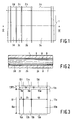
- Fig. 1 shows diagrammatically a division of electrodes 1, 2 between which an electro-optical material is present.
- the electrodes for example, a row electrode 1 and a column electrode 2 are divided into sub-electrodes 2 a , 2 b , 2 c , 2 d whose widths are in a ratio of 4 : 2 : 1 : 1.
- a display cell 3 is defined which can entirely or partly change its electro-optical properties by suitably driving the sub-electrodes.
- a liquid crystal is used as an electro-optical medium, it is possible to apply such a voltage to the (sub-)electrodes that a given voltage threshold is exceeded and the transmission state changes (locally), for example, from light absorbing to light transmissive, or conversely. This behaviour can also be determined in combination with the position of possibly present polarizers.
- the electrode 2 Since the electrode 2 is divided into sub-electrodes, it is possible to drive only a portion of the display cell 3.
- the portion 3 a of the display cell When the electrode 1 and sub-electrode 2 a are correctly energized, the portion 3 a of the display cell is driven so that this portion becomes, for example, light transmissive, whereas the other portion of the display cell remains opaque to light.
- the electrode 1 and sub-electrode 2 b are energized, the portion 3 b is driven, etc. In this way different surface areas of the display cell 3 can be driven so that different ratios of light transmissive/light opaque (white/black), in other words different grey scales are obtained.
- Fig. 2 is a diagrammatic cross-section of a part of the device taken on the line II-II in Fig. 1.
- the electrodes 1 and 2 are arranged as parallel strips of transmissive conductive material (for example, indium tin oxide) on transparent substrates 6, 7 of, for example, glass or quartz. As described above, said electrodes 1 and 2 are subdivided into column-sub electrodes 2 a , 2 b , 2 c , 2 d , while the row electrodes are also subdivided, if necessary. To give the liquid crystal molecules a given direction of preference at the area of the electrodes, the electrodes are coated with an electrically insulating or orienting layer 8. A layer of liquid crystal material 9, in this case a ferro-electric liquid crystal material is present between the two substrates 6, 7.
- the device can be used as a display device and will therefore be provided in a conventional manner with polarizers, colour filters and/or mirrors, as well as with an illumination system.
- the ferro-electric liquid crystal material has a bistable switching behaviour at the area of the sub-electrodes 2 a , 2 b , 2 c , so that the portions 3 a , 3 b , 3 c are exclusively switchable between two extreme states, namely substantially entirely transmissive and substantially entirely opaque (binary switching behaviour).
- the portion 3 d whose surface area is equal to the portion 3 c , is adjustable at, for example, four levels. This can be achieved by giving the display cell 3 at the area of the portion 3 d a gradual transmission/voltage characteristic with the aid of varying alternating voltages between the electrodes 1 and 2 d , as described in greater detail in EP-A- 0 402 984.
- the transmission for this portion 3 d is 0, 1/3aI, 2/3aI or aI. If the other portions 3 a , 3 b , 3 c of the display cell 3 d have surface areas of 4a, 2a and a, respectively, it is possible to adjust 8 transmission levels, namely 0, aI, 2aI, ... 7aI.
- the four values which are adjustable via the portion 3 d can then be superposed on these binary adjustable values so that a total of 32 transmission levels from 0 to 8aI is possible. This number is even higher for a larger number of adjustable levels. More generally, the number of grey scales is multiplied by a factor m by adding a single sub-pixel which can be adjusted at m different values. More generally, use of the invention leads to a total of 2 n-1 .m grey scales for the smallest sub-pixel with n sub-pixels and m different transmission values. Moreover, the grey scales are sharply defined in so far as they are exclusively determined by the binary adjustable values.
- the device of Figs. 1, 2 still has some shortcomings, because full drive of the portion 3 d of the display cell 3 leads to the same transmission level as driving the portion 3 c in the one extreme level.
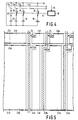
- the display cell 13 in the device of Fig. 3 has sub-cells 13 a , 13 b , 13 c , 13 d , 13 e , 13 f whose surface areas are in the ratio of 16 : 8 : 4 : 2 : 1 : (1-1/m) in which m is the number of transmission levels at which the portion 13 f of the display cell is adjustable.
- the portions of one display cell are now defined by row electrodes 11 and column electrodes 13 which are both divided into sub-electrodes (11 a , 11 b , and 12 a , 12 b , 12 c , respectively).
- the binary switchable portions 13 a , 13 b , 13 c are defined at the area of the row electrode 11 a and the column electrodes 11 a , 11 b , 11 c having a mutual width ratio of 4 : 2 : 1 at this area.
- the portions 13 d , 13 e are defined at the area of the row electrode 11 b having a mutual column width ratio of 2 : 1.
- the width ratio of the column electrodes at the area of the row electrode 11 a is 7 : 8 : 16.
- the transmitted (or blocked) quantity of light of the portion 13 f is thus 7/8 that of the light in the case of full drive of the portion 13 e , so that the above-mentioned possibility of driving one and the same grey scale in two manners no longer exists.
- the row electrode 11 b has a width which is approximately 1/8 of that of the total row width, which is advantageous from a lithographic point of view.
- the smallest sub-pixel can be situated in such a way that the optical point of gravity is in the centre of the pixel.
- the smallest sub-pixel is then surrounded by (parts of) the pixel which is the largest but one, and so forth; the other sub-pixels symmetrically surround the smallest sub-pixel.
- Fig. 4 shows diagrammatically an equivalent circuit diagram of the device of Fig. 3.
- An input circuit 15 converts an incoming signal 16 representing the information to be displayed into a plurality of drive signals 17.
- the drive signals 17 drive a plurality of switches 18 applying such a voltage to the portions 13 a , 13 b , 13 c , 13 d, 13 e that there is binary switching between such voltages (supplied by voltage sources 19 shown diagrammatically) that they switch between a fully transmissive state and a fully non-transmissive state.
- the drive signals 18 also control an adjustable resistor 20 which adjusts the portion 13 f of the pixel at one of the levels to be displayed, dependent on the signals presented.
- variable resistor instead of a variable resistor it is also possible to use, for example, a D/A converter.
- the drive signals then consist of, for example, an 8-bit signal whose 5 most significant bits determine the adjustments of the switches 18 and the 3 least significant bits determine the adjustment of the D/A converter.
- Fig. 5 shows sub-electrodes 23 a , 23 b , 23 c , 23 d , 23 e , 23 f of an actively driven display device complying with the desired surface ratios as described above and being connected via switching elements 24, not further referred to, to column electrodes 22 a , 22 b , 22 c .
- the sub-electrodes 23, switching elements 24 and column electrodes 22 are present on a first substrate.
- the row electrodes 21 a , 21 b are on a second substrate in this example, which together with the first substrate and a sealing edge defines a space filled with liquid crystal material.
- the device is provided in the conventional manner with colour filters, polarizers, etc.
- the display device has a gradual transmission/voltage characteristic which is adjustable at several values, while it is adjustable between two extreme values at the area of the other sub-electrodes. This is achieved by making use of, for example, a ferro-electric liquid crystalline medium which is subjected to an alternating voltage treatment at the area of sub-electrode 23 f .
- Use can be made again of twisted nematic liquid crystalline materials which are exlusively used between two extreme states at the area of the sub-electrodes 23 a , 23 b , 23 c , 23 d , 23 e .
Landscapes
- Engineering & Computer Science (AREA)
- Chemical & Material Sciences (AREA)
- Crystallography & Structural Chemistry (AREA)
- Physics & Mathematics (AREA)
- Computer Hardware Design (AREA)
- General Physics & Mathematics (AREA)
- Theoretical Computer Science (AREA)
- Liquid Crystal (AREA)
- Liquid Crystal Display Device Control (AREA)
- Devices For Indicating Variable Information By Combining Individual Elements (AREA)
Claims (8)
- Dispositif d'affichage comprenant un milieu électro-optique (9) entre deux plaques de support (6, 7), dans lequel des pixels (3) subdivisés en une pluralité de sous-pixels sont définis sur au moins une (7) des plaques de support à l'aide d'électrodes d'image (2, 12, 23), caractérisé en ce que dans chaque pixel, un sous-pixel (3d, 13f) a une aire de surface qui est au maximum égale à celle du plus petit des autres sous-pixels dudit pixel et est ajustable de manière analogique ou à une pluralité de m niveaux de transmission avec m > 2, tandis que les autres sous-pixels ont des aires de surfaces différentes et sont exclusivement commutables entre deux états de transmission extrêmes.
- Dispositif d'affichage selon la revendication 1, caractérisé en ce que lesdits autres sous-pixels ont un rapport de surfaces mutuelles de 2n:2n-1:... :2¹:2⁰.
- Dispositif d'affichage selon la revendication 1 ou 2, caractérisé en ce que le sous-pixel ajustable a une aire de surface qui est sensiblement de (1-1/m) fois l'aire de surface du plus petit des autres sous-pixels.
- Dispositif d'affichage selon l'une quelconque des revendications précédentes, caractérisé en ce que les pixels sont agencés en configuration matricielle et en ce qu'une pluralité de lignes de sélection (21) et de lignes de données (22) définissent les informations des sous-pixels (3, 13) via des dispositifs de commutation (24) qui commandent lesdits autres sous-pixels en binaire et commandent le sous-pixel ajustable de manière analogique ou avec une pluralité de m niveaux ajustables séparément avec m > 2.
- Dispositif d'affichage selon l'une quelconque des revendications 1 à 3, caractérisé en ce que les états de transmission intermédiaires et les états de transmission extrêmes sont ajustables via des éléments de commutation.
- Dispositif d'affichage selon l'une quelconque des revendications précédentes, caractérisé en ce que le milieu électro-optique est un cristal liquide ferroélectrique.
- Dispositif d'affichage selon l'une quelconque des revendications 1 à 5, caractérisé en ce que le sous-pixel ajustable est totalement ou partiellement entouré par les autres sous-pixels.
- Dispositif d'affichage selon la revendication 7, caractérisé en ce chaque sous-pixel est au moins partiellement entouré par un sous-pixel plus grand.
Applications Claiming Priority (2)
| Application Number | Priority Date | Filing Date | Title |
|---|---|---|---|
| NL9002011A NL9002011A (nl) | 1990-09-13 | 1990-09-13 | Weergeefinrichting. |
| NL9002011 | 1990-09-13 |
Publications (2)
| Publication Number | Publication Date |
|---|---|
| EP0478043A1 EP0478043A1 (fr) | 1992-04-01 |
| EP0478043B1 true EP0478043B1 (fr) | 1995-06-14 |
Family
ID=19857671
Family Applications (1)
| Application Number | Title | Priority Date | Filing Date |
|---|---|---|---|
| EP91202313A Expired - Lifetime EP0478043B1 (fr) | 1990-09-13 | 1991-09-10 | Ecran de visualisation |
Country Status (5)
| Country | Link |
|---|---|
| US (1) | US5208689A (fr) |
| EP (1) | EP0478043B1 (fr) |
| JP (1) | JP3022646B2 (fr) |
| DE (1) | DE69110387T2 (fr) |
| NL (1) | NL9002011A (fr) |
Families Citing this family (15)
| Publication number | Priority date | Publication date | Assignee | Title |
|---|---|---|---|---|
| KR940009449B1 (ko) * | 1991-04-06 | 1994-10-13 | 주식회사금성사 | 칼라비디오 프린터의 노광장치 |
| DE69225869T2 (de) * | 1991-11-19 | 1998-12-24 | Philips Electronics N.V., Eindhoven | Anzeigevorrichtung |
| JPH06102485A (ja) * | 1992-09-21 | 1994-04-15 | Canon Inc | 強誘電性液晶表示素子 |
| EP0740187B1 (fr) | 1995-04-28 | 2004-06-23 | Hewlett-Packard Company, A Delaware Corporation | Afficheur électro-optique |
| JPH1068931A (ja) * | 1996-08-28 | 1998-03-10 | Sharp Corp | アクティブマトリクス型液晶表示装置 |
| US6094187A (en) * | 1996-12-16 | 2000-07-25 | Sharp Kabushiki Kaisha | Light modulating devices having grey scale levels using multiple state selection in combination with temporal and/or spatial dithering |
| GB9626103D0 (en) * | 1996-12-16 | 1997-02-05 | Sharp Kk | Display/shutter devices |
| GB2325555A (en) * | 1997-05-20 | 1998-11-25 | Sharp Kk | Light modulating devices |
| US7053412B2 (en) * | 2003-06-27 | 2006-05-30 | The Trustees Of Princeton University And Universal Display Corporation | Grey scale bistable display |
| EP1697916A2 (fr) * | 2003-12-16 | 2006-09-06 | Koninklijke Philips Electronics N.V. | Panneau d'affichage à plasma comprenant une pluralite des pixels et un dispositif d'affichage |
| EP1650730B1 (fr) | 2004-10-25 | 2009-12-30 | Barco NV | Correction optique pour panneau lumineux d' uniformité élevée |
| US7639849B2 (en) | 2005-05-17 | 2009-12-29 | Barco N.V. | Methods, apparatus, and devices for noise reduction |
| US20080117231A1 (en) | 2006-11-19 | 2008-05-22 | Tom Kimpe | Display assemblies and computer programs and methods for defect compensation |
| GB201022137D0 (en) | 2010-12-31 | 2011-02-02 | Barco Nv | Display device and means to improve luminance uniformity |
| CN108254980A (zh) * | 2016-12-29 | 2018-07-06 | 南京瀚宇彩欣科技有限责任公司 | 全反射液晶显示面板 |
Citations (1)
| Publication number | Priority date | Publication date | Assignee | Title |
|---|---|---|---|---|
| EP0316774A2 (fr) * | 1987-11-12 | 1989-05-24 | Canon Kabushiki Kaisha | Appareil à cristaux à cristaux liquides |
Family Cites Families (4)
| Publication number | Priority date | Publication date | Assignee | Title |
|---|---|---|---|---|
| GB2217088A (en) * | 1988-04-05 | 1989-10-18 | English Electric Valve Co Ltd | Optical display panel |
| JP2700903B2 (ja) * | 1988-09-30 | 1998-01-21 | シャープ株式会社 | 液晶表示装置 |
| FR2637407B1 (fr) * | 1988-09-30 | 1994-02-11 | Commissariat A Energie Atomique | Procede d'affichage de niveaux de gris sur un ecran a cristaux liquides ferroelectriques a phase smectique chirale |
| DE3910418A1 (de) * | 1989-03-31 | 1990-10-04 | Licentia Gmbh | Anzeigevorrichtung |
-
1990
- 1990-09-13 NL NL9002011A patent/NL9002011A/nl not_active Application Discontinuation
-
1991
- 1991-08-19 US US07/747,218 patent/US5208689A/en not_active Expired - Fee Related
- 1991-09-10 EP EP91202313A patent/EP0478043B1/fr not_active Expired - Lifetime
- 1991-09-10 DE DE69110387T patent/DE69110387T2/de not_active Expired - Fee Related
- 1991-09-11 JP JP3231843A patent/JP3022646B2/ja not_active Expired - Lifetime
Patent Citations (1)
| Publication number | Priority date | Publication date | Assignee | Title |
|---|---|---|---|---|
| EP0316774A2 (fr) * | 1987-11-12 | 1989-05-24 | Canon Kabushiki Kaisha | Appareil à cristaux à cristaux liquides |
Also Published As
| Publication number | Publication date |
|---|---|
| JP3022646B2 (ja) | 2000-03-21 |
| DE69110387D1 (de) | 1995-07-20 |
| US5208689A (en) | 1993-05-04 |
| EP0478043A1 (fr) | 1992-04-01 |
| NL9002011A (nl) | 1992-04-01 |
| JPH04247431A (ja) | 1992-09-03 |
| DE69110387T2 (de) | 1996-02-22 |
Similar Documents
| Publication | Publication Date | Title |
|---|---|---|
| US5404236A (en) | Display device with crossing electrodes with specific ratio for gray scale | |
| EP0478043B1 (fr) | Ecran de visualisation | |
| EP0791848B1 (fr) | Afficheur et son procédé de commande | |
| EP0284134B1 (fr) | Méthode de commande d'un dispositif d'affichage à cristal liquide et dispositif d'affichage associé | |
| US7233304B1 (en) | Liquid crystal display apparatus | |
| US5671032A (en) | Ferroelectric liquid crystal device for gray scale display, gray scale display apparatus and method adopting the same | |
| US5689282A (en) | Display device with compensation for stray capacitance | |
| GB2130781A (en) | Liquid crystal colour display device | |
| US6201589B1 (en) | Spatial light modulator and display with picture elements having electrically floating electrodes | |
| KR960008099B1 (ko) | 매트릭스 디스플레이 장치 | |
| NL8703085A (nl) | Werkwijze voor het besturen van een weergeefinrichting. | |
| KR100326880B1 (ko) | 액정표시소자 | |
| KR100326436B1 (ko) | 광변조장치 | |
| EP0375269A2 (fr) | Dispositif d'affichage à cristal liquide | |
| KR100300552B1 (ko) | 광변조장치 | |
| JPH06324306A (ja) | 液晶表示装置 | |
| EP0543447B1 (fr) | Dispositif d'affichage | |
| JP2993016B2 (ja) | 液晶表示装置及びその駆動方法 | |
| JPH05249920A (ja) | 液晶表示装置の駆動回路 | |
| JP3332106B2 (ja) | 液晶表示装置 | |
| EP0600537A1 (fr) | Dispositif d'affichage | |
| JPH10311989A (ja) | 液晶表示素子 | |
| JPH04107526A (ja) | 階調表示用液晶駆動装置 | |
| JPH06214216A (ja) | 液晶表示装置の駆動回路 | |
| JPH055894A (ja) | 強誘電性液晶表示素子 |
Legal Events
| Date | Code | Title | Description |
|---|---|---|---|
| PUAI | Public reference made under article 153(3) epc to a published international application that has entered the european phase |
Free format text: ORIGINAL CODE: 0009012 |
|
| AK | Designated contracting states |
Kind code of ref document: A1 Designated state(s): DE FR GB IT NL |
|
| 17P | Request for examination filed |
Effective date: 19920924 |
|
| 17Q | First examination report despatched |
Effective date: 19940321 |
|
| GRAA | (expected) grant |
Free format text: ORIGINAL CODE: 0009210 |
|
| AK | Designated contracting states |
Kind code of ref document: B1 Designated state(s): DE FR GB IT NL |
|
| PG25 | Lapsed in a contracting state [announced via postgrant information from national office to epo] |
Ref country code: IT Free format text: LAPSE BECAUSE OF FAILURE TO SUBMIT A TRANSLATION OF THE DESCRIPTION OR TO PAY THE FEE WITHIN THE PRE;WARNING: LAPSES OF ITALIAN PATENTS WITH EFFECTIVE DATE BEFORE 2007 MAY HAVE OCCURRED AT ANY TIME BEFORE 2007. THE CORRECT EFFECTIVE DATE MAY BE DIFFERENT FROM THE ONE RECORDED.SCRIBED TIME-LIMIT Effective date: 19950614 Ref country code: NL Free format text: LAPSE BECAUSE OF NON-PAYMENT OF DUE FEES Effective date: 19950614 |
|
| REF | Corresponds to: |
Ref document number: 69110387 Country of ref document: DE Date of ref document: 19950720 |
|
| ET | Fr: translation filed | ||
| NLV1 | Nl: lapsed or annulled due to failure to fulfill the requirements of art. 29p and 29m of the patents act | ||
| PLBE | No opposition filed within time limit |
Free format text: ORIGINAL CODE: 0009261 |
|
| STAA | Information on the status of an ep patent application or granted ep patent |
Free format text: STATUS: NO OPPOSITION FILED WITHIN TIME LIMIT |
|
| 26N | No opposition filed | ||
| REG | Reference to a national code |
Ref country code: FR Ref legal event code: CD |
|
| PGFP | Annual fee paid to national office [announced via postgrant information from national office to epo] |
Ref country code: GB Payment date: 19990923 Year of fee payment: 9 |
|
| PGFP | Annual fee paid to national office [announced via postgrant information from national office to epo] |
Ref country code: FR Payment date: 19990928 Year of fee payment: 9 |
|
| PGFP | Annual fee paid to national office [announced via postgrant information from national office to epo] |
Ref country code: DE Payment date: 19991110 Year of fee payment: 9 |
|
| PG25 | Lapsed in a contracting state [announced via postgrant information from national office to epo] |
Ref country code: GB Free format text: LAPSE BECAUSE OF NON-PAYMENT OF DUE FEES Effective date: 20000910 |
|
| GBPC | Gb: european patent ceased through non-payment of renewal fee |
Effective date: 20000910 |
|
| PG25 | Lapsed in a contracting state [announced via postgrant information from national office to epo] |
Ref country code: FR Free format text: LAPSE BECAUSE OF NON-PAYMENT OF DUE FEES Effective date: 20010531 |
|
| PG25 | Lapsed in a contracting state [announced via postgrant information from national office to epo] |
Ref country code: DE Free format text: LAPSE BECAUSE OF NON-PAYMENT OF DUE FEES Effective date: 20010601 |
|
| REG | Reference to a national code |
Ref country code: FR Ref legal event code: ST |