EP0375869A2 - Verbindungstechnik und System für einen monolithischen Halbleiterchip - Google Patents
Verbindungstechnik und System für einen monolithischen Halbleiterchip Download PDFInfo
- Publication number
- EP0375869A2 EP0375869A2 EP89119542A EP89119542A EP0375869A2 EP 0375869 A2 EP0375869 A2 EP 0375869A2 EP 89119542 A EP89119542 A EP 89119542A EP 89119542 A EP89119542 A EP 89119542A EP 0375869 A2 EP0375869 A2 EP 0375869A2
- Authority
- EP
- European Patent Office
- Prior art keywords
- electric
- arrangement
- semiconductor chip
- terminations
- interconnection
- Prior art date
- Legal status (The legal status is an assumption and is not a legal conclusion. Google has not performed a legal analysis and makes no representation as to the accuracy of the status listed.)
- Withdrawn
Links
Images

Classifications
-
- H—ELECTRICITY
- H10—SEMICONDUCTOR DEVICES; ELECTRIC SOLID-STATE DEVICES NOT OTHERWISE PROVIDED FOR
- H10W—GENERIC PACKAGES, INTERCONNECTIONS, CONNECTORS OR OTHER CONSTRUCTIONAL DETAILS OF DEVICES COVERED BY CLASS H10
- H10W70/00—Package substrates; Interposers; Redistribution layers [RDL]
- H10W70/60—Insulating or insulated package substrates; Interposers; Redistribution layers
- H10W70/611—Insulating or insulated package substrates; Interposers; Redistribution layers for connecting multiple chips together
-
- H—ELECTRICITY
- H10—SEMICONDUCTOR DEVICES; ELECTRIC SOLID-STATE DEVICES NOT OTHERWISE PROVIDED FOR
- H10W—GENERIC PACKAGES, INTERCONNECTIONS, CONNECTORS OR OTHER CONSTRUCTIONAL DETAILS OF DEVICES COVERED BY CLASS H10
- H10W70/00—Package substrates; Interposers; Redistribution layers [RDL]
- H10W70/60—Insulating or insulated package substrates; Interposers; Redistribution layers
- H10W70/67—Insulating or insulated package substrates; Interposers; Redistribution layers characterised by their insulating layers or insulating parts
- H10W70/68—Shapes or dispositions thereof
- H10W70/685—Shapes or dispositions thereof comprising multiple insulating layers
-
- H—ELECTRICITY
- H10—SEMICONDUCTOR DEVICES; ELECTRIC SOLID-STATE DEVICES NOT OTHERWISE PROVIDED FOR
- H10W—GENERIC PACKAGES, INTERCONNECTIONS, CONNECTORS OR OTHER CONSTRUCTIONAL DETAILS OF DEVICES COVERED BY CLASS H10
- H10W90/00—Package configurations
- H10W90/701—Package configurations characterised by the relative positions of pads or connectors relative to package parts
- H10W90/721—Package configurations characterised by the relative positions of pads or connectors relative to package parts of bump connectors
- H10W90/724—Package configurations characterised by the relative positions of pads or connectors relative to package parts of bump connectors between a chip and a stacked insulating package substrate, interposer or RDL
Definitions
- the technical field of this invention is that of techniques and arrangements for completing electric circuits and systems of circuits in a single semiconductor chip, and particularly that of techniques and arrangements for establishing intra-chip connections between incomplete portions of electric circuits and systems fabricated on a single semiconductor chip.
- Semiconductor chips permit the microfabrication of electric circuits and systems of circuits (including subcircuits, portions of circuits, circuit elements, and components of circuits) on a single monolithic substrate containing an ever increasing density of circuits and systems. With an increase in the functionality of semiconductor chips, over recent years, the available surface area of semiconductor chips, remaining for interconnections to be made, is thus increasingly crowded.
- the invention herein is accordingly directed toward a layered, monolithic, semiconductor chip interconnection technique and arrangement adapted for interconnection of incomplete electric circuits, subcircuits, portions of circuits, circuit elements, and circuit components fabricated in a single semiconductor chip.
- the interconnection arrangement is surface mounted with solder bumps on the top surface of the semiconductor chip to be interconnected, establishing electrical connections between selected electric surface terminations at the respective top and bottom surfaces of the semiconductor chip and the interconnection arrangement.
- the interconnection technique includes establishing a predetermined scheme of electrically conductive paths on a selected substrate on which a plurality of conductive and insulative layers of material are fabricated in accordance with a predetermined interconnection scheme. This establishes a desired interconnection scheme which is effective to interconnect selected ones of the incomplete electric circuits and systems of circuits in the semiconductor chip, and electrically to close any gaps between portions of selected circuits on the chip.
- the monolithic interconnection arrangement is further particularly adapted to be solder mountable at predetermined electric surface termination pads on the semiconductor chip which is to be interconnected. Electric surface termination pads immediately adjacent to the edges of perimeter of the semiconductor chip are preferably reserved for making connection with other semiconductor chips. Such electric surface termination pads are typically not used for interconnections within the single semiconductor chip. However, according to the invention, any electrical top surface termination in a selected semiconductor chip can be interconnected as contemplated in the invention herein.
- Interconnection arrangements according to this invention need of course not operate in conjunction with each and every top surface termination fabricated into the semiconductor chip to be interconnected.
- a selected number of the top surface terminations may suffice to accomplish interconnection of particular circuits or subcircuits as desired.
- the electric terminations in the bottom surface of the interconnection arrangement are cooperatively patterned to be arranged in cooperation with the electric surface terminations on the top surface of the semiconductor chip subject to interconnection. This permits electrical communication between the interconnection arrangement and the semiconductor chip, which is effective for establishing selected interconnection schemes for electric circuits and systems of circuits in the semiconductor chip as desired.
- FIGs 1 and 2 show a semiconductor chip 13 and a monolithic interconnection arrangement 14 according to the invention herein, respectively electrically connected at electric surface terminations 13 ⁇ and 14 ⁇ , with electrically conductive solder bumps 16.
- monolithic interconnection arrangement 14 includes a bottom surface 14′
- semiconductor chip 13 includes a top surface 13′.
- the electric surface terminations 14 ⁇ of monolithic interconnection arrangement 14 are thus electrically connected with semiconductor chip 13 through solder bumps 16 and with a selected interconnection scheme defined within monolithic interconnection arrangement 14, which is shown in Figure 3 and which will be discussed in detail below.
- Semiconductor chip 13 shown in Figures 1 and 2 includes a substantially flat top surface 13′ having electric surface terminations 13 ⁇ fabricated in top surface 13′.
- the electric surface terminations 13 ⁇ in the top surface 13′ of semiconductor chip 13 are particularly shown in detail in Figure 2.
- These terminations 13 ⁇ are electrically connected across gaps in electric circuits or systems of circuits within semiconductor chip 13. These gaps render the particular electric circuits or systems of circuits in which they occur functionally incomplete.
- the gaps in these circuits or systems where intentionally fabricated in order to save space in the semiconductor ship 13, which would otherwise have been dedicated to rendering the circuits or systems complete.
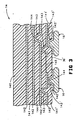
- FIG 3 shows the detailed construction of interconnection arrangement 14, including bottom surface 14′, electric surface terminations 14 ⁇ , a substrate 140, insulative layers 141, conductive layers 142, and vias 143 for interconnecting adjacent conductive layers 142, in partial vertical cross-sectional detail, particularly illustrating the plurality of layered conductive and insulative layers which form interconnection paths and regions to implement desired interconnection schemes between selected ones of bumps 16 and the electric surface terminations 13 ⁇ in semiconductor chip 13.
- interconnection arrangement 14 includes a plurality of insulative and conductive layers respectively 141 and 142 at successive levels within interconnection arrangement 14, fabricated according to techniques well known in the art.
- Conductive and insulative layers 141 and 142 are regionally patterned to establish conductive paths between respective ones of electric surface terminations 14 ⁇ in the bottom surface 14′ of the interconnection arrangement 14, effectively to guide the flow and application of electric currents and voltages, as needed to accomplish specific, desired electrical interconnections in semiconductor chip 13.
- the conductive layers 142 can be joined through vias 143 which extend through insulative layers 141 in the interconnection arrangement 14. In particular, at selected locations 144 in arrangement 14, the conductive layers 142 extend through adjacent insulative layers 141 to form electrical paths for establishing particular interconnections.
- Figure 3 additionally shows a gap 145 between a selected conductive layer 142 at a predetermined level of interconnection arrangement 14, a technique which can be employed to ensure desired separation of multiple electrical paths between electric surface terminations 14 ⁇ in interconnection arrangement 14.
- electrically conductive bumps 16 are formed on a lowest one of conductive layers 142, in particular conductive layer 142′, which is provided with a localized coating of a barrier metal such as chromium, on the portions of the bottom surface 14′ of interconnection arrangement 14 at which it is known that bumps 16 are desirably emplaced.
- the chromium material included in conductive layer 142′ extends in a via 143′ through the lowermost of insulative layers 141, that is layer 141′, electrically to be able to communicate with respective solder bumps 16.
- Electrically conductive layer 142′ may according to one version of the invention include tungsten or aluminum material, and the chromium included in layer 142′ ensures that no leeching of solder in bumps 16 into conductive layer 142′ will occur.
- Bumps 16 are interconnected with interconnection arrangement 14 along selected electrical paths defined within interconnection arrangement 14 through particular regions of conductive and insulative layers, 142 and 141, respectively. This permits electrical communication through bumps 16 and along selected paths in interconnection arrangement 14 through conductive layers 142 interconnected through one or more levels of insulative layers 141 to establish a desired interconnection scheme for incomplete circuits or systems in semiconductor chip 13.
- Figure 3 shows two bumps 16 respectively joined with first and second electrical surface terminations 14 ⁇ in the bottom surface 14′ of interconnection arrangement 14.
- the paths in interconnection arrangement 14 may include a plurality of selected electric circuits and circuit components (e.g., capacitors and/or resistors) at one or more levels of interconnection arrangement 14.
- the particular number of bumps 16 employed with interconnection arrangement 14 depends upon the particular interconnection arrangement scheme selected.
- a particular interconnection arrangement 14 may include any number of electrically conductive bumps 16, for electrical communion with electric surface terminations 13 ⁇ in the top surface 13′ of a semiconductor chip 13, as shown in Figure 2, depending upon the number of electrical circuits, subcircuits, portions of circuits, circuit components, and circuit elements to be interconnected.
- Interconnection arrangement 14 may contain multipolar circuit elements (e.g. transistors, resistors or capacitors), as well as complex interconnections which may themselves require more than merely two bumps 16 for electrical communication with a semiconductor chip 13, to be interconnected. Bumps 16 are particularly effective to engage electric surface terminations 13 ⁇ and 14 ⁇ in the respective top and bottom surfaces, 13′ and 14′, of semiconductor chip 13 and interconnection arrangement 14. These electrical surface terminations 13 ⁇ and 14 ⁇ are manufactured in accordance with techniques well known to those skilled in the art to which this invention pertains. For example, plated metal ceramic techniques can be employed in the manufacture of interconnect arrangement 14. In accordance with this technique, interconnection arrangement 14 may thus respectively include a substrate 140 and insulating layers 141 of aluminum or aluminum nitride, and respective conductive layers 142 of tungsten or aluminum.
- multipolar circuit elements e.g. transistors, resistors or capacitors
- Interconnection arrangement 14 can further be manufactured according to well known techniques with a substrate 140 of silicon wafer, glass, sapphire, or ceramic material.
- the insulative material used for insulative layers 144 can be of fabricated of silicon-oxide or polyamide material, for example.
- the material of conductive layers 142 can also be plated copper or aluminum, for example. If a multi-layer ceramic interconnection arrangement 14 is desired, then substrate 140 and insulative layers 141 are for example made of alumina or aluminum nitride material. The conductive material in conductive layers 142 is then tungsten material for example.
- Bumps 16 are preferably made of Pb-Sn solder material, which bonds particularly well to a local region which has been pretreated with a large concentration of chromium at the point of desired joinder, i.e., at respective electric terminations 13 ⁇ and 14 ⁇ to ensure effective bonding.
- Mounting of the interconnection arrangement 14 in place upon the semiconductor chip 13 subject to interconnection is, for example, accomplished by positioning or placement of bumps 16 upon each of electric surface terminations 13 ⁇ or 14 ⁇ , positioning interconnection arrangement 14 and electric surface terminations 14 ⁇ over corresponding electric surface terminations 13 ⁇ , and heating the combination up to 300 to 400 degrees Celsius, for a suitable period of time until adjacent, cooperative electric surface terminations 13 ⁇ and 14 ⁇ are joined.
- this interconnection arrangement 14 and technique permits substantially increased circuit density on semiconductor chips 13 to be achieved.
- This scheme of interconnection saves considerably large areas of semiconductor chip real estate for fabrication of circuits, thereby endowing semiconductor chip 13 with increased functionality.
- a monolithic semiconductor chip interconnection arrangement 14 is thus established to accomplish desired interconnections in the circuitry of a semiconductor chip 13 which includes one or more incomplete electric circuits or systems of circuits.
Landscapes
- Internal Circuitry In Semiconductor Integrated Circuit Devices (AREA)
- Semiconductor Integrated Circuits (AREA)
Applications Claiming Priority (2)
| Application Number | Priority Date | Filing Date | Title |
|---|---|---|---|
| US07/290,496 US5021869A (en) | 1988-12-27 | 1988-12-27 | Monolithic semiconductor chip interconnection technique and arrangement |
| US290496 | 1988-12-27 |
Publications (2)
| Publication Number | Publication Date |
|---|---|
| EP0375869A2 true EP0375869A2 (de) | 1990-07-04 |
| EP0375869A3 EP0375869A3 (de) | 1991-04-17 |
Family
ID=23116271
Family Applications (1)
| Application Number | Title | Priority Date | Filing Date |
|---|---|---|---|
| EP19890119542 Withdrawn EP0375869A3 (de) | 1988-12-27 | 1989-10-20 | Verbindungstechnik und System für einen monolithischen Halbleiterchip |
Country Status (3)
| Country | Link |
|---|---|
| US (1) | US5021869A (de) |
| EP (1) | EP0375869A3 (de) |
| JP (1) | JPH02222146A (de) |
Cited By (3)
| Publication number | Priority date | Publication date | Assignee | Title |
|---|---|---|---|---|
| EP0475269A3 (en) * | 1990-09-10 | 1992-10-14 | Hitachi, Ltd. | Integrated circuit device comprising a wiring substrate |
| EP0503201A3 (de) * | 1990-12-20 | 1994-03-16 | Toshiba Kk | |
| US5907786A (en) * | 1992-11-11 | 1999-05-25 | Mitsubishi Denki Kabushiki Kaisha | Process for manufacturing a flip-chip integrated circuit |
Families Citing this family (4)
| Publication number | Priority date | Publication date | Assignee | Title |
|---|---|---|---|---|
| JP2688446B2 (ja) * | 1990-03-26 | 1997-12-10 | 株式会社日立製作所 | 多層配線基板およびその製造方法 |
| US5783483A (en) * | 1993-02-24 | 1998-07-21 | Intel Corporation | Method of fabricating a barrier against metal diffusion |
| US6222212B1 (en) | 1994-01-27 | 2001-04-24 | Integrated Device Technology, Inc. | Semiconductor device having programmable interconnect layers |
| US6576848B1 (en) * | 1996-11-22 | 2003-06-10 | International Business Machines Corporation | Integrated circuit chip wiring structure with crossover capability and method of manufacturing the same |
Family Cites Families (7)
| Publication number | Priority date | Publication date | Assignee | Title |
|---|---|---|---|---|
| US3634731A (en) * | 1970-08-06 | 1972-01-11 | Atomic Energy Commission | Generalized circuit |
| GB1487945A (en) * | 1974-11-20 | 1977-10-05 | Ibm | Semiconductor integrated circuit devices |
| US4074342A (en) * | 1974-12-20 | 1978-02-14 | International Business Machines Corporation | Electrical package for lsi devices and assembly process therefor |
| GB8506714D0 (en) * | 1985-03-15 | 1985-04-17 | Smiths Industries Plc | Electronic circuit assemblies |
| JPH0714105B2 (ja) * | 1986-05-19 | 1995-02-15 | 日本電装株式会社 | 混成集積回路基板及びその製造方法 |
| JPH07112041B2 (ja) * | 1986-12-03 | 1995-11-29 | シャープ株式会社 | 半導体装置の製造方法 |
| US4731700A (en) * | 1987-02-12 | 1988-03-15 | Delco Electronics Corporation | Semiconductor connection and crossover apparatus |
-
1988
- 1988-12-27 US US07/290,496 patent/US5021869A/en not_active Expired - Lifetime
-
1989
- 1989-10-20 EP EP19890119542 patent/EP0375869A3/de not_active Withdrawn
- 1989-12-26 JP JP1338063A patent/JPH02222146A/ja active Pending
Cited By (11)
| Publication number | Priority date | Publication date | Assignee | Title |
|---|---|---|---|---|
| EP0475269A3 (en) * | 1990-09-10 | 1992-10-14 | Hitachi, Ltd. | Integrated circuit device comprising a wiring substrate |
| US5212403A (en) * | 1990-09-10 | 1993-05-18 | Hitachi, Ltd. | Integrated circuit device having an ic chip mounted on the wiring substrate and having suitable mutual connections between internal circuits |
| EP0503201A3 (de) * | 1990-12-20 | 1994-03-16 | Toshiba Kk | |
| US5473514A (en) * | 1990-12-20 | 1995-12-05 | Kabushiki Kaisha Toshiba | Semiconductor device having an interconnecting circuit board |
| US5613295A (en) * | 1990-12-20 | 1997-03-25 | Kabushiki Kaisha Toshiba | Semiconductor device having an interconnecting circuit board and method for manufacturing same |
| US5646830A (en) * | 1990-12-20 | 1997-07-08 | Kabushiki Kaisha Toshiba | Semiconductor device having an interconnecting circuit board |
| US5715147A (en) * | 1990-12-20 | 1998-02-03 | Kabushiki Kaisha Toshiba | Semiconductor device having an interconnecting circuit board |
| US5907786A (en) * | 1992-11-11 | 1999-05-25 | Mitsubishi Denki Kabushiki Kaisha | Process for manufacturing a flip-chip integrated circuit |
| US6204566B1 (en) | 1992-11-11 | 2001-03-20 | Mitsubishi Denki Kabushiki Kaisha | Resin encapsulated electrode structure of a semiconductor device, mounted semiconductor devices, and semiconductor wafer including multiple electrode structures |
| US6284554B1 (en) | 1992-11-11 | 2001-09-04 | Mitsubishi Denki Kabushiki Kaisha | Process for manufacturing a flip-chip integrated circuit |
| US6469397B2 (en) | 1992-11-11 | 2002-10-22 | Mitsubishi Denki Kabushiki Kaisha | Resin encapsulated electrode structure of a semiconductor device, mounted semiconductor devices, and semiconductor wafer including multiple electrode structures |
Also Published As
| Publication number | Publication date |
|---|---|
| JPH02222146A (ja) | 1990-09-04 |
| US5021869A (en) | 1991-06-04 |
| EP0375869A3 (de) | 1991-04-17 |
Similar Documents
| Publication | Publication Date | Title |
|---|---|---|
| US5475264A (en) | Arrangement having multilevel wiring structure used for electronic component module | |
| CN105514077B (zh) | 具有引线接合件的功率覆层结构和制造其的方法 | |
| US5132613A (en) | Low inductance side mount decoupling test structure | |
| EP0526456B1 (de) | Mehrschichtpackung mit einer vertieften höhlung für einen halbleiter-chip | |
| US5488542A (en) | MCM manufactured by using thin film multilevel interconnection technique | |
| US5578525A (en) | Semiconductor device and a fabrication process thereof | |
| EP0197089B1 (de) | Integrierter zusammenbau auf einer halbleiterscheibe | |
| US5874782A (en) | Wafer with elevated contact structures | |
| US6724611B1 (en) | Multi-layer chip capacitor | |
| US4991000A (en) | Vertically interconnected integrated circuit chip system | |
| EP0393220B1 (de) | Integrierte Schaltungspackung | |
| US4945399A (en) | Electronic package with integrated distributed decoupling capacitors | |
| JP4592122B2 (ja) | パッケージ層の数を削減したフリップチップ・パッケージ | |
| US4926241A (en) | Flip substrate for chip mount | |
| US7129574B2 (en) | Multi-power ring chip scale package for system level integration | |
| US4710798A (en) | Integrated circuit chip package | |
| US5673478A (en) | Method of forming an electronic device having I/O reroute | |
| US20090065937A1 (en) | Structure of high performance combo chip and processing method | |
| US7829997B2 (en) | Interconnect for chip level power distribution | |
| WO1992003844A1 (en) | Multilayer integrated circuit module | |
| JP2974159B2 (ja) | 薄膜再分配域を備えた多層モジュール | |
| US5021869A (en) | Monolithic semiconductor chip interconnection technique and arrangement | |
| US6888218B2 (en) | Embedded capacitor multi-chip modules | |
| US6031258A (en) | High DC current stagger power/ground pad | |
| US6444919B1 (en) | Thin film wiring scheme utilizing inter-chip site surface wiring |
Legal Events
| Date | Code | Title | Description |
|---|---|---|---|
| PUAI | Public reference made under article 153(3) epc to a published international application that has entered the european phase |
Free format text: ORIGINAL CODE: 0009012 |
|
| AK | Designated contracting states |
Kind code of ref document: A2 Designated state(s): DE FR GB |
|
| PUAL | Search report despatched |
Free format text: ORIGINAL CODE: 0009013 |
|
| AK | Designated contracting states |
Kind code of ref document: A3 Designated state(s): DE FR GB |
|
| 17P | Request for examination filed |
Effective date: 19910918 |
|
| 17Q | First examination report despatched |
Effective date: 19930825 |
|
| STAA | Information on the status of an ep patent application or granted ep patent |
Free format text: STATUS: THE APPLICATION IS DEEMED TO BE WITHDRAWN |
|
| 18D | Application deemed to be withdrawn |
Effective date: 19940105 |