EP0376045A2 - Verfahren und Einrichtung zur Verarbeitung einer feinen Struktur - Google Patents
Verfahren und Einrichtung zur Verarbeitung einer feinen Struktur Download PDFInfo
- Publication number
- EP0376045A2 EP0376045A2 EP89122906A EP89122906A EP0376045A2 EP 0376045 A2 EP0376045 A2 EP 0376045A2 EP 89122906 A EP89122906 A EP 89122906A EP 89122906 A EP89122906 A EP 89122906A EP 0376045 A2 EP0376045 A2 EP 0376045A2
- Authority
- EP
- European Patent Office
- Prior art keywords
- sample
- needle
- gas
- atom
- molecule
- Prior art date
- Legal status (The legal status is an assumption and is not a legal conclusion. Google has not performed a legal analysis and makes no representation as to the accuracy of the status listed.)
- Granted
Links
Images







Classifications
-
- C—CHEMISTRY; METALLURGY
- C23—COATING METALLIC MATERIAL; COATING MATERIAL WITH METALLIC MATERIAL; CHEMICAL SURFACE TREATMENT; DIFFUSION TREATMENT OF METALLIC MATERIAL; COATING BY VACUUM EVAPORATION, BY SPUTTERING, BY ION IMPLANTATION OR BY CHEMICAL VAPOUR DEPOSITION, IN GENERAL; INHIBITING CORROSION OF METALLIC MATERIAL OR INCRUSTATION IN GENERAL
- C23C—COATING METALLIC MATERIAL; COATING MATERIAL WITH METALLIC MATERIAL; SURFACE TREATMENT OF METALLIC MATERIAL BY DIFFUSION INTO THE SURFACE, BY CHEMICAL CONVERSION OR SUBSTITUTION; COATING BY VACUUM EVAPORATION, BY SPUTTERING, BY ION IMPLANTATION OR BY CHEMICAL VAPOUR DEPOSITION, IN GENERAL
- C23C16/00—Chemical coating by decomposition of gaseous compounds, without leaving reaction products of surface material in the coating, i.e. chemical vapour deposition [CVD] processes
- C23C16/44—Chemical coating by decomposition of gaseous compounds, without leaving reaction products of surface material in the coating, i.e. chemical vapour deposition [CVD] processes characterised by the method of coating
- C23C16/455—Chemical coating by decomposition of gaseous compounds, without leaving reaction products of surface material in the coating, i.e. chemical vapour deposition [CVD] processes characterised by the method of coating characterised by the method used for introducing gases into reaction chamber or for modifying gas flows in reaction chamber
- C23C16/45523—Pulsed gas flow or change of composition over time
- C23C16/45525—Atomic layer deposition [ALD]
- C23C16/45544—Atomic layer deposition [ALD] characterized by the apparatus
-
- B—PERFORMING OPERATIONS; TRANSPORTING
- B82—NANOTECHNOLOGY
- B82B—NANOSTRUCTURES FORMED BY MANIPULATION OF INDIVIDUAL ATOMS, MOLECULES, OR LIMITED COLLECTIONS OF ATOMS OR MOLECULES AS DISCRETE UNITS; MANUFACTURE OR TREATMENT THEREOF
- B82B3/00—Manufacture or treatment of nanostructures by manipulation of individual atoms or molecules, or limited collections of atoms or molecules as discrete units
-
- B—PERFORMING OPERATIONS; TRANSPORTING
- B82—NANOTECHNOLOGY
- B82Y—SPECIFIC USES OR APPLICATIONS OF NANOSTRUCTURES; MEASUREMENT OR ANALYSIS OF NANOSTRUCTURES; MANUFACTURE OR TREATMENT OF NANOSTRUCTURES
- B82Y30/00—Nanotechnology for materials or surface science, e.g. nanocomposites
-
- B—PERFORMING OPERATIONS; TRANSPORTING
- B82—NANOTECHNOLOGY
- B82Y—SPECIFIC USES OR APPLICATIONS OF NANOSTRUCTURES; MEASUREMENT OR ANALYSIS OF NANOSTRUCTURES; MANUFACTURE OR TREATMENT OF NANOSTRUCTURES
- B82Y40/00—Manufacture or treatment of nanostructures
-
- C—CHEMISTRY; METALLURGY
- C23—COATING METALLIC MATERIAL; COATING MATERIAL WITH METALLIC MATERIAL; CHEMICAL SURFACE TREATMENT; DIFFUSION TREATMENT OF METALLIC MATERIAL; COATING BY VACUUM EVAPORATION, BY SPUTTERING, BY ION IMPLANTATION OR BY CHEMICAL VAPOUR DEPOSITION, IN GENERAL; INHIBITING CORROSION OF METALLIC MATERIAL OR INCRUSTATION IN GENERAL
- C23C—COATING METALLIC MATERIAL; COATING MATERIAL WITH METALLIC MATERIAL; SURFACE TREATMENT OF METALLIC MATERIAL BY DIFFUSION INTO THE SURFACE, BY CHEMICAL CONVERSION OR SUBSTITUTION; COATING BY VACUUM EVAPORATION, BY SPUTTERING, BY ION IMPLANTATION OR BY CHEMICAL VAPOUR DEPOSITION, IN GENERAL
- C23C16/00—Chemical coating by decomposition of gaseous compounds, without leaving reaction products of surface material in the coating, i.e. chemical vapour deposition [CVD] processes
- C23C16/04—Coating on selected surface areas, e.g. using masks
- C23C16/047—Coating on selected surface areas, e.g. using masks using irradiation by energy or particles
-
- C—CHEMISTRY; METALLURGY
- C23—COATING METALLIC MATERIAL; COATING MATERIAL WITH METALLIC MATERIAL; CHEMICAL SURFACE TREATMENT; DIFFUSION TREATMENT OF METALLIC MATERIAL; COATING BY VACUUM EVAPORATION, BY SPUTTERING, BY ION IMPLANTATION OR BY CHEMICAL VAPOUR DEPOSITION, IN GENERAL; INHIBITING CORROSION OF METALLIC MATERIAL OR INCRUSTATION IN GENERAL
- C23C—COATING METALLIC MATERIAL; COATING MATERIAL WITH METALLIC MATERIAL; SURFACE TREATMENT OF METALLIC MATERIAL BY DIFFUSION INTO THE SURFACE, BY CHEMICAL CONVERSION OR SUBSTITUTION; COATING BY VACUUM EVAPORATION, BY SPUTTERING, BY ION IMPLANTATION OR BY CHEMICAL VAPOUR DEPOSITION, IN GENERAL
- C23C16/00—Chemical coating by decomposition of gaseous compounds, without leaving reaction products of surface material in the coating, i.e. chemical vapour deposition [CVD] processes
- C23C16/44—Chemical coating by decomposition of gaseous compounds, without leaving reaction products of surface material in the coating, i.e. chemical vapour deposition [CVD] processes characterised by the method of coating
- C23C16/455—Chemical coating by decomposition of gaseous compounds, without leaving reaction products of surface material in the coating, i.e. chemical vapour deposition [CVD] processes characterised by the method of coating characterised by the method used for introducing gases into reaction chamber or for modifying gas flows in reaction chamber
- C23C16/45523—Pulsed gas flow or change of composition over time
- C23C16/45525—Atomic layer deposition [ALD]
- C23C16/45527—Atomic layer deposition [ALD] characterized by the ALD cycle, e.g. different flows or temperatures during half-reactions, unusual pulsing sequence, use of precursor mixtures or auxiliary reactants or activations
- C23C16/45536—Use of plasma, radiation or electromagnetic fields
-
- G—PHYSICS
- G03—PHOTOGRAPHY; CINEMATOGRAPHY; ANALOGOUS TECHNIQUES USING WAVES OTHER THAN OPTICAL WAVES; ELECTROGRAPHY; HOLOGRAPHY
- G03F—PHOTOMECHANICAL PRODUCTION OF TEXTURED OR PATTERNED SURFACES, e.g. FOR PRINTING, FOR PROCESSING OF SEMICONDUCTOR DEVICES; MATERIALS THEREFOR; ORIGINALS THEREFOR; APPARATUS SPECIALLY ADAPTED THEREFOR
- G03F1/00—Originals for photomechanical production of textured or patterned surfaces, e.g., masks, photo-masks, reticles; Mask blanks or pellicles therefor; Containers specially adapted therefor; Preparation thereof
- G03F1/68—Preparation processes not covered by groups G03F1/20 - G03F1/50
- G03F1/82—Auxiliary processes, e.g. cleaning or inspecting
- G03F1/84—Inspecting
- G03F1/86—Inspecting by charged particle beam [CPB]
-
- G—PHYSICS
- G11—INFORMATION STORAGE
- G11B—INFORMATION STORAGE BASED ON RELATIVE MOVEMENT BETWEEN RECORD CARRIER AND TRANSDUCER
- G11B9/00—Recording or reproducing using a method not covered by one of the main groups G11B3/00 - G11B7/00; Record carriers therefor
- G11B9/12—Recording or reproducing using a method not covered by one of the main groups G11B3/00 - G11B7/00; Record carriers therefor using near-field interactions; Record carriers therefor
- G11B9/14—Recording or reproducing using a method not covered by one of the main groups G11B3/00 - G11B7/00; Record carriers therefor using near-field interactions; Record carriers therefor using microscopic probe means, i.e. recording or reproducing by means directly associated with the tip of a microscopic electrical probe as used in Scanning Tunneling Microscopy [STM] or Atomic Force Microscopy [AFM] for inducing physical or electrical perturbations in a recording medium; Record carriers or media specially adapted for such transducing of information
-
- H—ELECTRICITY
- H01—ELECTRIC ELEMENTS
- H01J—ELECTRIC DISCHARGE TUBES OR DISCHARGE LAMPS
- H01J37/00—Discharge tubes with provision for introducing objects or material to be exposed to the discharge, e.g. for the purpose of examination or processing thereof
- H01J37/30—Electron-beam or ion-beam tubes for localised treatment of objects
- H01J37/305—Electron-beam or ion-beam tubes for localised treatment of objects for casting, melting, evaporating, or etching
- H01J37/3053—Electron-beam or ion-beam tubes for localised treatment of objects for casting, melting, evaporating, or etching for evaporating or etching
- H01J37/3056—Electron-beam or ion-beam tubes for localised treatment of objects for casting, melting, evaporating, or etching for evaporating or etching for microworking, e. g. etching of gratings or trimming of electrical components
-
- H—ELECTRICITY
- H10—SEMICONDUCTOR DEVICES; ELECTRIC SOLID-STATE DEVICES NOT OTHERWISE PROVIDED FOR
- H10P—GENERIC PROCESSES OR APPARATUS FOR THE MANUFACTURE OR TREATMENT OF DEVICES COVERED BY CLASS H10
- H10P95/00—Generic processes or apparatus for manufacture or treatments not covered by the other groups of this subclass
-
- B—PERFORMING OPERATIONS; TRANSPORTING
- B82—NANOTECHNOLOGY
- B82Y—SPECIFIC USES OR APPLICATIONS OF NANOSTRUCTURES; MEASUREMENT OR ANALYSIS OF NANOSTRUCTURES; MANUFACTURE OR TREATMENT OF NANOSTRUCTURES
- B82Y10/00—Nanotechnology for information processing, storage or transmission, e.g. quantum computing or single electron logic
-
- Y—GENERAL TAGGING OF NEW TECHNOLOGICAL DEVELOPMENTS; GENERAL TAGGING OF CROSS-SECTIONAL TECHNOLOGIES SPANNING OVER SEVERAL SECTIONS OF THE IPC; TECHNICAL SUBJECTS COVERED BY FORMER USPC CROSS-REFERENCE ART COLLECTIONS [XRACs] AND DIGESTS
- Y10—TECHNICAL SUBJECTS COVERED BY FORMER USPC
- Y10S—TECHNICAL SUBJECTS COVERED BY FORMER USPC CROSS-REFERENCE ART COLLECTIONS [XRACs] AND DIGESTS
- Y10S148/00—Metal treatment
- Y10S148/045—Electric field
-
- Y—GENERAL TAGGING OF NEW TECHNOLOGICAL DEVELOPMENTS; GENERAL TAGGING OF CROSS-SECTIONAL TECHNOLOGIES SPANNING OVER SEVERAL SECTIONS OF THE IPC; TECHNICAL SUBJECTS COVERED BY FORMER USPC CROSS-REFERENCE ART COLLECTIONS [XRACs] AND DIGESTS
- Y10—TECHNICAL SUBJECTS COVERED BY FORMER USPC
- Y10S—TECHNICAL SUBJECTS COVERED BY FORMER USPC CROSS-REFERENCE ART COLLECTIONS [XRACs] AND DIGESTS
- Y10S977/00—Nanotechnology
- Y10S977/84—Manufacture, treatment, or detection of nanostructure
- Y10S977/849—Manufacture, treatment, or detection of nanostructure with scanning probe
- Y10S977/855—Manufacture, treatment, or detection of nanostructure with scanning probe for manufacture of nanostructure
-
- Y—GENERAL TAGGING OF NEW TECHNOLOGICAL DEVELOPMENTS; GENERAL TAGGING OF CROSS-SECTIONAL TECHNOLOGIES SPANNING OVER SEVERAL SECTIONS OF THE IPC; TECHNICAL SUBJECTS COVERED BY FORMER USPC CROSS-REFERENCE ART COLLECTIONS [XRACs] AND DIGESTS
- Y10—TECHNICAL SUBJECTS COVERED BY FORMER USPC
- Y10S—TECHNICAL SUBJECTS COVERED BY FORMER USPC CROSS-REFERENCE ART COLLECTIONS [XRACs] AND DIGESTS
- Y10S977/00—Nanotechnology
- Y10S977/84—Manufacture, treatment, or detection of nanostructure
- Y10S977/849—Manufacture, treatment, or detection of nanostructure with scanning probe
- Y10S977/855—Manufacture, treatment, or detection of nanostructure with scanning probe for manufacture of nanostructure
- Y10S977/856—Manufacture, treatment, or detection of nanostructure with scanning probe for manufacture of nanostructure including etching/cutting
-
- Y—GENERAL TAGGING OF NEW TECHNOLOGICAL DEVELOPMENTS; GENERAL TAGGING OF CROSS-SECTIONAL TECHNOLOGIES SPANNING OVER SEVERAL SECTIONS OF THE IPC; TECHNICAL SUBJECTS COVERED BY FORMER USPC CROSS-REFERENCE ART COLLECTIONS [XRACs] AND DIGESTS
- Y10—TECHNICAL SUBJECTS COVERED BY FORMER USPC
- Y10S—TECHNICAL SUBJECTS COVERED BY FORMER USPC CROSS-REFERENCE ART COLLECTIONS [XRACs] AND DIGESTS
- Y10S977/00—Nanotechnology
- Y10S977/84—Manufacture, treatment, or detection of nanostructure
- Y10S977/849—Manufacture, treatment, or detection of nanostructure with scanning probe
- Y10S977/855—Manufacture, treatment, or detection of nanostructure with scanning probe for manufacture of nanostructure
- Y10S977/857—Manufacture, treatment, or detection of nanostructure with scanning probe for manufacture of nanostructure including coating
-
- Y—GENERAL TAGGING OF NEW TECHNOLOGICAL DEVELOPMENTS; GENERAL TAGGING OF CROSS-SECTIONAL TECHNOLOGIES SPANNING OVER SEVERAL SECTIONS OF THE IPC; TECHNICAL SUBJECTS COVERED BY FORMER USPC CROSS-REFERENCE ART COLLECTIONS [XRACs] AND DIGESTS
- Y10—TECHNICAL SUBJECTS COVERED BY FORMER USPC
- Y10S—TECHNICAL SUBJECTS COVERED BY FORMER USPC CROSS-REFERENCE ART COLLECTIONS [XRACs] AND DIGESTS
- Y10S977/00—Nanotechnology
- Y10S977/84—Manufacture, treatment, or detection of nanostructure
- Y10S977/849—Manufacture, treatment, or detection of nanostructure with scanning probe
- Y10S977/855—Manufacture, treatment, or detection of nanostructure with scanning probe for manufacture of nanostructure
- Y10S977/859—Manufacture, treatment, or detection of nanostructure with scanning probe for manufacture of nanostructure including substrate treatment
-
- Y—GENERAL TAGGING OF NEW TECHNOLOGICAL DEVELOPMENTS; GENERAL TAGGING OF CROSS-SECTIONAL TECHNOLOGIES SPANNING OVER SEVERAL SECTIONS OF THE IPC; TECHNICAL SUBJECTS COVERED BY FORMER USPC CROSS-REFERENCE ART COLLECTIONS [XRACs] AND DIGESTS
- Y10—TECHNICAL SUBJECTS COVERED BY FORMER USPC
- Y10S—TECHNICAL SUBJECTS COVERED BY FORMER USPC CROSS-REFERENCE ART COLLECTIONS [XRACs] AND DIGESTS
- Y10S977/00—Nanotechnology
- Y10S977/84—Manufacture, treatment, or detection of nanostructure
- Y10S977/849—Manufacture, treatment, or detection of nanostructure with scanning probe
- Y10S977/86—Scanning probe structure
- Y10S977/868—Scanning probe structure with optical means
- Y10S977/869—Optical microscope
-
- Y—GENERAL TAGGING OF NEW TECHNOLOGICAL DEVELOPMENTS; GENERAL TAGGING OF CROSS-SECTIONAL TECHNOLOGIES SPANNING OVER SEVERAL SECTIONS OF THE IPC; TECHNICAL SUBJECTS COVERED BY FORMER USPC CROSS-REFERENCE ART COLLECTIONS [XRACs] AND DIGESTS
- Y10—TECHNICAL SUBJECTS COVERED BY FORMER USPC
- Y10S—TECHNICAL SUBJECTS COVERED BY FORMER USPC CROSS-REFERENCE ART COLLECTIONS [XRACs] AND DIGESTS
- Y10S977/00—Nanotechnology
- Y10S977/84—Manufacture, treatment, or detection of nanostructure
- Y10S977/849—Manufacture, treatment, or detection of nanostructure with scanning probe
- Y10S977/86—Scanning probe structure
- Y10S977/875—Scanning probe structure with tip detail
Definitions
- the present invention relates to a method and apparatus for processing a fine pattern to provide a structure in the unit of an atom or molecule such as film formation and processing of patterns of ultra-fine structures.
- Examples are the fabrication and correction of ultra-fine patterns such as LSI and patterns of various structures such as molecular devices and bioelements.
- the pattern of a semiconductor integrated circuit is becoming more and more fine every year, and the related lithography mask drawing technique, the defect correcting technique and the technique for correcting integrated circuit patterns formed thereby, also have a requirement to become finer.
- the minimum spot diameter has encountered a lower limit of 50 nm or so even when focusing is made at a high magnification using a multi-stage lens.
- the molecular electronics element uses a molecule as a switching element as one limit of element attenuation.
- the bioelement is constituted by living body related molecules and employs molecules like those in a living body as an information transfer medium by combining molecules of A order having function.
- Scanning tunneling microscopes are known for observation of atoms of a sample and have also been suggested for atomic scale surface modification by atom removal or the like as disclosed in Japanese Patent Application Laid-Open No. 63-92025 having a Laid-Open date of April 23, 1963 and in "Atomic-scale surface modifications using a tunneling microscope", Becker et al, Nature, Vol. 325, January 29, 1987, pp. 419-421.
- Such disclosures are not directed to processing of a fine pattern to correct a defect or the like therein or to form a film nor to the processing of molecular devices.
- a method and apparatus for processing an ultra-fine pattern utilizes a scanning tunneling microscope system. More specifically, if a scanning tunneling microscope with a needle having a sharp tip is drawn close to a sample surface to be processed at a distance of about 1 nm or less and voltage is applied between the sample and the needle, there will flow a tunnel current therebetween. If the distance is 3 nm or more, there will flow a field emission current. In this case, the tunnel current will flow between the atoms in the needle tip and the sample surface, and the field emission current will spread only several nm on the sample surface because of an extremely short distance. Thus, by various processes using this electric current, processing, alteration or film formation of an ultra-fine pattern, or removing and adding operations in the unit of an atom or molecule are enabled.
- the fine pattern processing apparatus is an improved processing apparatus utilizing a scanning tunneling microscope (STM), shown generally in Fig. 2, and capable of directly observing atoms one by one.
- STM scanning tunneling microscope
- Fig. 3 illustrates a tunnel current creating phenomenon, in which the numeral 1123 denotes an electron cloud. If voltage from a power source 119 (Fig.
- a tunnel current will flow.
- This current is extremely sensitive to the change in distance between the two. It changes as much as one decimal place for a change in distance of 0.1 nm. Further, if the gap distance is 3 nm or more, a field emission current will flow. In this case, the tunnel current will flow between the atoms in the needle tip and the sample surface and the field emission current will spread only several nm on the sample surface because of an extremely short distance.
- the STM utilizes a three-dimensional piezoelectric actuator 100 having three piezoelectric actuators.
- X, Y piezoelectric actuators 101 and 102 are driven by an X-Y scanning circuit 116 while maintaining constant the tunnel current detected by a tunnel current amplifier 118.
- the tunnel current detected from the tunnel current amplifier 118 increases, and a servo-circuit 117 drives a Z piezoelectric actuator 103 to raise the needle 108 until the original current is obtained.
- the needle 108 is lowered in response to the change in the detected tunnel current.
- the up and down movements of the needle 108 applied to the piezoelectric actuator 103 correspond to concave and convex portions of the surface of the sample 107. That is, signals applied to a memory 120 from the servo-circuit 117 correspond to those surface concave and convex portions.
- signals applied to a memory 120 from the servo-circuit 117 correspond to those surface concave and convex portions.
- the X-Y scanning circuit 116 to the memory 120 there are applied X-Y displacement signals corresponding to X-Y driving signals applied to the piezoelectric actuators 101 and 102.
- the voltage changes applied to the piezoelectric actuators 101, 102 and 103 are stored in the memory 120, and a microcomputer 121 reads out the data stored in the memory 120, images the data and displays the image on a display unit 122, whereby the surface structure of the sample material can be observed on an atomic scale.
- the tunnel current is in the range of about 1 to 10 nA.
- the possibility of damage is small because the power applied to the sample 107 is as low as 1 pW to 1 nW.
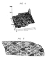
- Fig. 4 shows a topographic map of the structure of an atomic scale of a Si surface obtained by such method. Atoms are reflected one by one in concave and convex portions.
- Fig. 5 represents a contour line map of an STM image of a Si surface.
- Fig. 1 shows a basic construction of the scanning tunneling type fine pattern processing apparatus.
- the three-dimensional actuator 100 of the tunnel unit actuates the X-Y scanning circuit 116 and the Z drive and servo circuit 117, which issue driving signals to drive the piezoelectric actuators 101, 102 and 103 in X, Y and Z directions, respectively, thereby causing the needle portion 105 fixed thereto to effect minute movement in X, Y, Z directions.
- An XY stage controller 115 causes a stage 106 to perform a coarse movement by controlling drive mechanisms 123X, 123Y and motors 124X, 124Y on the basis of a command provided from the microcomputer 121 and positional data of the stage 106 measured by a laser length measuring unit 109 which is controlled by a laser length measuring unit controller 110.
- the position control for the stage 106 is performed by the XY stage controller 115 so that the command (target position) from the microcomputer 121 corresponds to a precise position data of the stage obtained from the controller 110.
- the laser length measuring unit controller 110 measures precise position data of the stage by using the laser length measuring unit 130, mirrors 132, 133, 134, 135, and a deflecting prism 131.
- a gas atmosphere is formed between the sample 107 and the needle 108 and a tunnel current or a field radiation current flows therebetween, causing the atoms or molecules of the gas to be radicalized, ionized or excited by electron collision, whereby the sample 107 can be subjected to sputtering, chemical etching or CVD film formation in the order of one to several atoms or molecules.
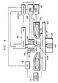
- Fig. 6 shows another embodiment of a fine pattern processing apparatus of a scanning tunneling type.
- the tunnel current or the field emission current flowing between the needle 108 of the needle portion 105 attached to the actuator 100 constituted by piezoelectric actuators (X, Y, Z directions), and the sample 107 spreads and is radiated to a wide area of the sample as shown by broken line 605a.
- the apparatus shown in Fig. 6 prevents such spreading.
- the scanning tunneling type fine pattern processing apparatus is provided with a lens and deflector utilizing a magnetic field or electric field to focus or deflect the tunnel current or the field emission current.
- Fig. 6 illustrates the apparatus provided with a magnetic field lens and deflector.
- the numeral 618 denotes a magnetic pole
- numeral 106 denotes a sample carrier stage
- numeral 610 denotes a magnetic pole of a focusing lens
- numeral 611 denotes a coil thereof
- numeral 609 denotes a coil power source B.
- Numerals 607 and 608 may be a focusing lens and a power source thereof, or may be a deflector and a power source thereof.
- the tunnel current or the field emission current is focused by the magnetic poles 607, 610, 618 and the intensity of magnetism provided thereto, and is radiated as a focused beam 605b to the sample 107, whereby it is made possible to effect radiation of electric current, detection and processing for a very narrow area of the sample which area is from 1 nm or less to several atoms, one atom or less.
- the degree of focusing of the above focused beam can be changed by changing the intensity of magnetic field provided to the magnetic poles 607, 610, 618 by means of the coil power sources 608 and 609, and hence the irradiation region can be changed.
- members 606 and 607 serve as deflectors
- the deflection of the beam is performed thereby, and in place of moving the actuator 100, the beam is slightly deflected, thereby permitting positioning with high accuracy and scanning at high speed. If the apparatus is constructed so that the magnetic poles and coils 607, 606, 610, 611, 606, 618 move together with the actuator 100 and the needle portion 105, it is possible to align the axes of these systems always with the axis of the needle.
- the coil power sources 608 and 609 are controlled by a controller 617 (it is apparent that the microcomputer 121 may be used), whereby it is made possible to control the strengths of these components with respect to each other or impart a picture drawing function thereto. In these cases, even if electrostatic type deflectors, lenses, and power sources for them are used in place of the electromagnetic type deflectors, lenses, and power sources, it is possible to achieve the same focusing as shown by the focused beam 605b.
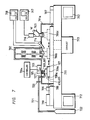
- Fig. 7 shows a scanning tunneling type fine pattern processing apparatus according to a further embodiment of the present invention.
- This apparatus includes a surface plate 711 mounted on a deoscillating base 712 such as an air servo mount, a vacuum vessel 711a mounted on the surface plate 711, a sample carrier stage 706 mounted on the vacuum vessel 711a and movable to positions represented by 706a, 706b and 706c, a scanning tunneling unit 701 (as shown in Fig. 1 and 6) provided with a needle portion 105 having a needle 108 and also provided with a piezoelectric actuator 100 and controller 701a, an SEM (scanning electron microscope) 702 and an optical microscope 703.
- a deoscillating base 712 such as an air servo mount
- a vacuum vessel 711a mounted on the surface plate 711
- a sample carrier stage 706 mounted on the vacuum vessel 711a and movable to positions represented by 706a, 706b and 706c
- the sample carrier stage 706 is moved by a driving portion 707 and can take a position 706a of the scanning tunneling unit, a position 706b for observation by SEM and a position 706c for observation by an optical microscope.
- To the tunneling unit 701 are attached focusing and deflecting poles and coils 606, 607, 610, 611 (as shown in Fig. 6) to focus or deflect the beam of tunnel current or field emission current.
- the stage position can be measured and set at a high accuracy of 0.1 ⁇ m or less by means of a laser length measuring unit 710, a polarizing prism 709, a window 708 and a mirror 708a attached to the sample carrier stage 706.
- a gas nozzle 727 for enabling gas to be blown to the vicinity of the needle 108 of the scanning tunneling unit 701 from a gas cylinder 722 through a pipe 721 and a valve 720 which serves for turning on and off gas flow and gas flow adjustment.
- gases may be utilized including organometallic compound gases, polymer gases such as silane, and reactive gases such as halogen and compounds thereof.
- the sample is placed in the vacuum vessel 711a through a loader chamber (not shown), and exhaustion is performed by a vacuum exhaustion system 713.
- the sample carrier stage is moved to the position 706c, and a desired part of the sample 107 is detected by direct observation through a window or the optical microscope 703 or by observation through them and further through a camera 716 and a display 717.
- the sample carrier 706 is moved to the position 706b of the SEM 702 and a secondary electron emitted from the sample 107 is detected by a detector 714 on the basis of the rough observation made by the optical microscope 703, and the result of the detection is displayed on a display 718. In this way minute observation and positioning are performed.
- the sample carrier stage 706 is transferred to the position 706a and a finer detection is performed by microscopic observation using the scanning tunneling unit 701, whereby positioning is made finally to an atom, a group of atoms or a molecule to be processed, to which there can be applied a processing such as removal, adhesion or speed-up etching.
- the resolving power of detection can be successively increased from the order of ⁇ m with the optical microscope 703, to 10 - 1 nm with the SEM 702, and to 0.1 - 0.01 nm by driving the piezoelectric actuators 101, 102 and 103 using the scanning tunneling unit XY scanning circuit 116 and the Z drive and servo circuit 117, detecting a tunnel current or a field emission current by the current amplifier 118 and displaying the result of the detection on the display 122 through the processing made by the microcomputer 121, as shown in Fig. 1. Since the observation area and the resolving power overlap between the optical microscope and the SEM and between the SEM and the scanning tunneling microscope, the operations up to the positioning of atomic order can be performed continuously from the field of vision of the optical microscope by using the arrangement described above.
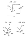
- Figs. 8(a) to 8(c) illustrate the details of processing of atomic or molecular order, i.e., in units of an atom or molecule, carried out by the present invention.
- Fig. 8(a) shows a state wherein the needle 108 of the needle portion 105 is drawn close to the surface of the sample 107, voltage is applied between the two by the power source 119 and a tunnel current or a field emission current 801 flows.
- Fig. 8(b) shows the state of a tip 802 of the needle 108 and a surface 803 of the sample 107. More specifically, the tunnel current is discharged from an atom 802a of the needle tip 802 with respect to an atom 804a of the sample and an electron 806 is emitted. As a result, the atom 804a and nearby atoms 804b, 804c are removed by the resulting energy to form a hole 805 of such an atomic or molecular level as shown in Fig. 8(c).
- Fig. 9(a) shows the case where processing is effected for an insulating material 902 formed as the sample 107 on an electroconductive substrate 901. Also in this case, if the insulating film is sufficiently thin, the surface of the insulating material 902 will be polarized by a polarization effect induced by the voltage applied between the needle 108 and the electroconductive substrate 901, whereby a tunnel current or a field emission current flows to permit processing of the insulating film material 902 as the sample 107.
- electrode plates 903 for polarization are mounted around the needle 108 for enhancing the polarization effect.
- Voltage is applied to the polarizing electrode plates 903 independently of the needle 108 by means of a power source 904 to polarize the insulating material 902 in advance. In this state, voltage is applied to the needle 108 by means of a power source 119 to facilitate tunnel current or field emission current flow as described with respect to Fig. 9(a).
- Fig. 10 shows the case where gas is blown from the nozzle 727 to the vicinity of the tip of the needle 108 of the needle portion 105 as shown in Fig. 7. More specifically as shown in Fig. 19(a), gas 1001 is blown from the gas nozzle 727 to the vicinity of the needle 108 and of the portion of the sample 107 opposed to the needle, and in this state voltage is applied from the power source 119 and a tunnel current or a field emission current flows.
- a metallic compound for CVD chemical vapor deposition
- an organometallic compound examples of which include metal-alkyl compounds such as Ai(CH3)3, Al(C2H5)3, Al(C4H9)3, Cd(CH3)2 and Cd(C2H5)2, metal-carbonyl compounds such as M(CnH 2n+1 )m and MO(CO)6, metal-alkoxide compounds such as M(CO)N and TaO(C2H5)5, M(OCH 2n+1 )m, and metal halides, i.e. MXn such as WF6 and WCl6 wherein M is a metal element, e.g.
- W, Mo, Ta, Al, Cd, Zn, Ni, or Zr, m and n are each an integer
- X is a halogen element such as, for example, F, Cl, or Br, this substance is subject to the action of the tunnel current or the field emission current and is decomposed by the energy of the current so that a metal atom is separated and adheres to the surface 803 of the sample 803 in the position 1002 as shown in Fig. 10(b). At this time, as shown in Fig.
- FIG. 10(d) shows that a large number of atoms can be adhered onto an area 1006 by scanning the tip 802 of the needle 108 in the direction of arrow 1004 with respect to the sample 107, then moving the tip by one atom in the direction of arrow 1005, further moving it in the direction of arrow 1004 and repeating this process. In this manner, a film layer of such atoms is formed in a specified area.
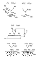
- Fig. 11(a) shows the case where reactive gases such as halogen and halogen compound gases, e.g., fluorine, chlorine, CCl4, CF4 are blown out from the nozzle 727.
- gases such as halogen and halogen compound gases, e.g., fluorine, chlorine, CCl4, CF4 are blown out from the nozzle 727.
- Molecules of these gases indicated at 1101 and 11022, are decomposed or activated by a tunnel current or a field emission current flowing between the tip 802 of the needle 108 and the surface 803 of the sample 107, and are thereby bonded to sample atoms to form volatile atoms 1103 and 1104, which volatilize to form hole 1105 as shown in Fig. 11(b), thus permitting a high-speed removal.
- Fig. 12 shows an example of local annealing performed by the scanning tunneling type fine pattern processing apparatus of the present invention.
- the sample 107 has an impurity 1202 implanted in a substrate 1201 of a semiconductor, for example, by ion implantation.
- the impurity 1202a, 1202b, 1202c, as shown in Fig. 12(b) is not electrically activated due to the presence of a lattice defect or the remaining of internal strain.
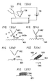
- Fig. 13 shows a further example of processing in accordance with the present invention.
- the polarity of the power source 119 is reversed and positive and negative voltages are applied to the needle 108 and the sample 107, respectively.
- an electron flows not from an atom of the tip 802 of the needle 108, as shown in Fig. 8, but rather the electron 1301 flows from the surface portion 803 of the sample 107, which is close to the needle, toward the needle tip 802.
- gas atoms 1302a and 1302b are ionized by the action of the flowing electron.
- An ion 1303 thus formed flows to the surface 803 of the sample 107 to which is applied a negative voltage, as shown in Fig. 13(a), and it adheres as a gas atom 1304 onto the sample surface 803, as shown in Fig. 13(d).
- the needle 108 and the sample 107 are moved in a relative manner by the actuator 100 of a piezoelectric element for example, to scan the needle tip 802 in two dimensions in the direction of arrows 1004 and 1005 on the sample surface, as shown in Fig. 13(e), there is formed a wide gas atom adhered area 1305 on the surface 803 of the sample 107.
- atoms can be laminated as a multi-layer film 1306 as shown in Fig. 13(f).
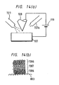
- Fig. 14(a) by providing plural gas nozzles 727, 727a and flowing two or more kinds of gases alternately from those nozzles, there can be laminated in multi-layers different kinds of atomic layers represented by a layer or layers 1306 of atoms from the first nozzle 727 and a layer or layers 1307 of atoms from the second nozzle 727a, as shown in Fig. 14(b).
- Fig. 15 shows another processing method utilizing the arrangement of Fig. 15(a).
- an electron 1301 emitted from the surface 803 of the sample 107 ionizes a gas atom 1302 and the resulting ion 1303 adheres to the sample surface 803.
- the compound 1503 vaporizes as shown in Fig. 15(e) and an atom 1503 is removed from the sample surface 803 to form a cut-out portion (processed hole) 1504.
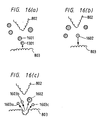
- a heavy element 1601 is used as a gas atom emitted from the nozzle 727 in the apparatus illustrated in Fig. 15(a).
- This atom is ionized by the action of an electron 1301 emitted from the sample surface 803 and the resulting heavy ion indicated at 1602 in Fig. 16(b) advances toward the sample surface to which a negative voltage is applied.
- the resulting collision induces a sputtering action, whereby sample atoms 1603a, 1603b, 1603c. 7-8 are emitted and removed as shown in Fig. 16(c).
- Fig. 17(a) shows an embodiment for repositioning atoms or molecules of the sample 107 in the unit of an atom by using a device provided with a power source 1701 having a switch capable of changing over from one polarity to another polarity. More specifically, if the switch of the power source 1701 is held in the state of A, B and negative and positive voltages are applied to the needle 108 and the sample 107, respectively, an electron 806 flows from the needle tip to the sample surface, as shown in Fig. 17(b). By this action an atom 804 of the sample surface 803 is ionized into a positive ion 807 as shown in Fig. 17(c), which moves toward the needle tip 802 as shown in Fig.
- the removed atom can be adhered to a predetermined position by being moved in the X and Y directions by control of the piezoelectric element actuator.
- a molecular device or a biodevice an element is formed basically by linkage or combination of atoms or molecules, and the technique for separating or altering that linkage is important in the correction of poor characteristics or analysis of the element. That is, in molecular devices and biodevices, the removal and connection in the unit of an atom or molecular are extremely important.
- Fig. 18(a) illustrates a NAND current having two inputs A and B and an output, with Fig. 18(b) illustrating the equivalent molecular electronic device using molecules for switching as proposed by F. Carter in Physics, 10D, 1984, pp. 175.
- this molecular device works as a NAND circuit and such a fine molecular device can be integrated in a density of 106 higher than the usual semiconductor devices.
Landscapes
- Chemical & Material Sciences (AREA)
- Engineering & Computer Science (AREA)
- Physics & Mathematics (AREA)
- Nanotechnology (AREA)
- Crystallography & Structural Chemistry (AREA)
- Materials Engineering (AREA)
- General Physics & Mathematics (AREA)
- General Chemical & Material Sciences (AREA)
- Organic Chemistry (AREA)
- Chemical Kinetics & Catalysis (AREA)
- Mechanical Engineering (AREA)
- Metallurgy (AREA)
- Plasma & Fusion (AREA)
- Manufacturing & Machinery (AREA)
- Condensed Matter Physics & Semiconductors (AREA)
- Analytical Chemistry (AREA)
- Composite Materials (AREA)
- Electromagnetism (AREA)
- Toxicology (AREA)
- Health & Medical Sciences (AREA)
- Measurement Of Length, Angles, Or The Like Using Electric Or Magnetic Means (AREA)
- Shaping Of Tube Ends By Bending Or Straightening (AREA)
- Cold Cathode And The Manufacture (AREA)
- Drying Of Semiconductors (AREA)
- Internal Circuitry In Semiconductor Integrated Circuit Devices (AREA)
- Preparing Plates And Mask In Photomechanical Process (AREA)
- ing And Chemical Polishing (AREA)
Applications Claiming Priority (3)
| Application Number | Priority Date | Filing Date | Title |
|---|---|---|---|
| JP325768/88 | 1988-12-26 | ||
| JP32576888 | 1988-12-26 | ||
| JP63325768A JPH02173278A (ja) | 1988-12-26 | 1988-12-26 | 微細加工方法及びその装置 |
Publications (3)
| Publication Number | Publication Date |
|---|---|
| EP0376045A2 true EP0376045A2 (de) | 1990-07-04 |
| EP0376045A3 EP0376045A3 (de) | 1991-01-16 |
| EP0376045B1 EP0376045B1 (de) | 2001-05-16 |
Family
ID=18180407
Family Applications (1)
| Application Number | Title | Priority Date | Filing Date |
|---|---|---|---|
| EP89122906A Expired - Lifetime EP0376045B1 (de) | 1988-12-26 | 1989-12-12 | Verfahren und Einrichtung zur Verarbeitung einer feinen Struktur |
Country Status (5)
| Country | Link |
|---|---|
| US (1) | US5116782A (de) |
| EP (1) | EP0376045B1 (de) |
| JP (1) | JPH02173278A (de) |
| KR (1) | KR930001494B1 (de) |
| DE (1) | DE68929298T2 (de) |
Cited By (14)
| Publication number | Priority date | Publication date | Assignee | Title |
|---|---|---|---|---|
| EP0480183A3 (en) * | 1990-10-09 | 1992-06-10 | International Business Machines Corporation | Method and apparatus for writing or etching narrow linewidth patterns on insulating materials |
| EP0459392A3 (en) * | 1990-05-30 | 1992-12-09 | Hitachi, Ltd. | Method and apparatus for processing a minute portion of a specimen |
| GB2267997A (en) * | 1992-06-19 | 1993-12-22 | Hitachi Europ Ltd | Atomic scale devices |
| EP0522168A4 (de) * | 1991-01-11 | 1994-08-31 | Hitachi, Ltd. | |
| DE4342314A1 (de) * | 1993-12-11 | 1995-06-14 | Joachim Behrendt | Verfahren zur Erzeugung von Strukturen |
| NL9401925A (nl) * | 1993-12-01 | 1995-07-03 | Integrated Circuit Testing | Werkwijze en inrichting voor het bewerken van een monster. |
| EP0687889A3 (de) * | 1994-06-16 | 1996-10-16 | Japan Res Dev Corp | Verfahren zur Feststellung der Atomverschiebung auf Materieoberflächen und Verfahren zur lokalen Zuführung von Heteroatomen |
| WO1999008099A1 (de) * | 1997-08-05 | 1999-02-18 | Institut für Festkörper- und Werkstofforschung Dresden e.V. | Verfahren zum auftragen oder abtragen von materialien |
| EP1292361A4 (de) * | 2000-05-26 | 2004-07-07 | Univ Northwestern | Verfahren mittels abtastenden mikroskopspritzen und produkte dafür oder dadurch erzeugt |
| EP1012584A4 (de) * | 1997-01-21 | 2006-10-04 | Rave L L C | Vorrichtung zur kontrollie und/oder veränderung von gegenständen. |
| EP1724639A3 (de) * | 2005-05-16 | 2007-12-26 | ASML Netherlands B.V. | Imprint-Lithografie |
| US7485856B2 (en) | 1994-07-28 | 2009-02-03 | General Nanotechnology Llp | Scanning probe microscopy inspection and modification system |
| US7535817B2 (en) | 1995-07-24 | 2009-05-19 | General Nanotechnology, L.L.C. | Nanometer scale data storage device and associated positioning system |
| US7615738B2 (en) | 1994-07-28 | 2009-11-10 | General Nanotechnology, Llc | Scanning probe microscope assembly and method for making spectrophotometric, near-field, and scanning probe measurements |
Families Citing this family (29)
| Publication number | Priority date | Publication date | Assignee | Title |
|---|---|---|---|---|
| EP0483867A3 (en) * | 1990-11-01 | 1993-01-27 | Matsushita Electric Industrial Co., Ltd | Method of discharge processing of semiconductor |
| WO2004081684A1 (ja) * | 1991-11-29 | 2004-09-23 | Ryuji Takada | 圧電素子の駆動方法及び装置並びに微動機構の制御装置 |
| US5444260A (en) * | 1993-07-01 | 1995-08-22 | Midwest Reasearch Institute | Atomic-level imaging, processing and characterization of semiconductor surfaces |
| US5512218A (en) * | 1994-03-24 | 1996-04-30 | Cambridge Scientific, Inc. | Method of making biopolymer-based nonlinear optical materials |
| JP3721440B2 (ja) * | 1995-08-24 | 2005-11-30 | 三洋電機株式会社 | 層状物質材料の加工方法 |
| US6369397B1 (en) * | 1999-01-04 | 2002-04-09 | International Business Machines Corporation | SPM base focal plane positioning |
| KR20010062924A (ko) * | 1999-12-21 | 2001-07-09 | 박종섭 | 액정표시장치의 결함 리페어 장치 |
| US6640459B1 (en) * | 2001-02-15 | 2003-11-04 | Fast Forward Devices, Llc | Multidimensional contact mechanics measurement system |
| US6937447B2 (en) | 2001-09-19 | 2005-08-30 | Kabushiki Kaisha Toshiba | Magnetoresistance effect element, its manufacturing method, magnetic reproducing element and magnetic memory |
| WO2003083948A1 (en) * | 2002-03-28 | 2003-10-09 | Wennan Din | Molecular integrated circuit molecular electronic devices |
| DE10226382B4 (de) * | 2002-06-13 | 2004-05-19 | Carl Zeiss | Kataraktchirurgie-Mikroskopiesystem und Verfahren hierzu |
| US20040121069A1 (en) * | 2002-08-08 | 2004-06-24 | Ferranti David C. | Repairing defects on photomasks using a charged particle beam and topographical data from a scanning probe microscope |
| ATE390562T1 (de) * | 2004-11-19 | 2008-04-15 | Ebm Papst St Georgen Gmbh & Co | Anordnung mit einem luefter und einer pumpe |
| EP1842228A4 (de) * | 2005-01-10 | 2010-03-10 | Bioforce Nanosciences Inc | System und verfahren zur erzeugung einer oberflächenstruktur |
| JP2007299880A (ja) * | 2006-04-28 | 2007-11-15 | Toshiba Corp | 磁気抵抗効果素子,および磁気抵抗効果素子の製造方法 |
| JP5044157B2 (ja) * | 2006-07-11 | 2012-10-10 | 株式会社東芝 | 磁気抵抗効果素子,磁気ヘッド,および磁気再生装置 |
| JP2008085220A (ja) * | 2006-09-28 | 2008-04-10 | Toshiba Corp | 磁気抵抗効果素子、磁気ヘッド、および磁気再生装置 |
| WO2009120342A1 (en) * | 2008-03-24 | 2009-10-01 | The Board Of Trustees Of The Leland Stanford Junior University | Method for stm assisted ald |
| US8296859B2 (en) * | 2008-03-24 | 2012-10-23 | The Board Of Trustees Of The Leland Stanford Junior University | Prototyping station for atomic force microscope-assisted deposition of nanostructures |
| JP5032430B2 (ja) * | 2008-09-26 | 2012-09-26 | 株式会社東芝 | 磁気抵抗効果素子の製造方法、磁気抵抗効果素子、磁気ヘッドアセンブリ及び磁気記録再生装置 |
| JP5032429B2 (ja) * | 2008-09-26 | 2012-09-26 | 株式会社東芝 | 磁気抵抗効果素子の製造方法、磁気抵抗効果素子、磁気ヘッドアセンブリ及び磁気記録再生装置 |
| JP5039006B2 (ja) | 2008-09-26 | 2012-10-03 | 株式会社東芝 | 磁気抵抗効果素子の製造方法、磁気抵抗効果素子、磁気ヘッドアセンブリ及び磁気記録再生装置 |
| JP5039007B2 (ja) * | 2008-09-26 | 2012-10-03 | 株式会社東芝 | 磁気抵抗効果素子の製造方法、磁気抵抗効果素子、磁気ヘッドアセンブリ及び磁気記録再生装置 |
| JP2011210492A (ja) * | 2010-03-29 | 2011-10-20 | Sii Nanotechnology Inc | 集束イオンビーム装置 |
| MX357200B (es) * | 2012-05-07 | 2018-06-29 | Univ Ottawa | Fabricacion de nanoporos utilizando campos electricos elevados. |
| US9564291B1 (en) * | 2014-01-27 | 2017-02-07 | Mochii, Inc. | Hybrid charged-particle beam and light beam microscopy |
| US10811214B2 (en) * | 2019-01-18 | 2020-10-20 | Applied Materials, Inc. | Low emission cladding and ion implanter |
| US12437965B1 (en) * | 2022-08-01 | 2025-10-07 | Mochil, Inc. | Charged-particle beam microscope with differential vacuum pressures |
| CN117800285B (zh) * | 2024-03-01 | 2024-05-17 | 浙江大学 | 一种环境气氛下多能场诱导原子级数控加工装置及方法 |
Family Cites Families (8)
| Publication number | Priority date | Publication date | Assignee | Title |
|---|---|---|---|---|
| CH643397A5 (de) * | 1979-09-20 | 1984-05-30 | Ibm | Raster-tunnelmikroskop. |
| US4495377A (en) * | 1982-12-30 | 1985-01-22 | International Business Machines Corporation | Substrate wiring patterns for connecting to integrated-circuit chips |
| US4539089A (en) * | 1984-06-29 | 1985-09-03 | International Business Machines Corporation | Method for depositing material with nanometer dimensions |
| US4550257A (en) * | 1984-06-29 | 1985-10-29 | International Business Machines Corporation | Narrow line width pattern fabrication |
| US4724318A (en) * | 1985-11-26 | 1988-02-09 | International Business Machines Corporation | Atomic force microscope and method for imaging surfaces with atomic resolution |
| JPS6326936A (ja) * | 1986-07-18 | 1988-02-04 | Jeol Ltd | 走査トンネル顕微鏡 |
| JPS6392025A (ja) * | 1986-10-06 | 1988-04-22 | Mitsubishi Electric Corp | 導電性材料加工装置 |
| JPH0640001B2 (ja) * | 1987-04-23 | 1994-05-25 | 日本電子株式会社 | 走査トンネル顕微鏡 |
-
1988
- 1988-12-26 JP JP63325768A patent/JPH02173278A/ja active Pending
-
1989
- 1989-12-12 EP EP89122906A patent/EP0376045B1/de not_active Expired - Lifetime
- 1989-12-12 DE DE68929298T patent/DE68929298T2/de not_active Expired - Fee Related
- 1989-12-22 KR KR1019890019233A patent/KR930001494B1/ko not_active Expired - Fee Related
- 1989-12-22 US US07/455,155 patent/US5116782A/en not_active Expired - Lifetime
Cited By (21)
| Publication number | Priority date | Publication date | Assignee | Title |
|---|---|---|---|---|
| EP0459392A3 (en) * | 1990-05-30 | 1992-12-09 | Hitachi, Ltd. | Method and apparatus for processing a minute portion of a specimen |
| US5214282A (en) * | 1990-05-30 | 1993-05-25 | Hitachi, Ltd. | Method and apparatus for processing a minute portion of a specimen |
| EP0480183A3 (en) * | 1990-10-09 | 1992-06-10 | International Business Machines Corporation | Method and apparatus for writing or etching narrow linewidth patterns on insulating materials |
| US5689494A (en) * | 1991-01-11 | 1997-11-18 | Hitachi, Ltd. | Surface atom fabrication method and apparatus |
| US5416331A (en) * | 1991-01-11 | 1995-05-16 | Hitachi, Ltd. | Surface atom fabrication method and apparatus |
| EP0522168A4 (de) * | 1991-01-11 | 1994-08-31 | Hitachi, Ltd. | |
| GB2267997B (en) * | 1992-06-19 | 1996-08-28 | Hitachi Europ Ltd | Atomic scale devices |
| GB2267997A (en) * | 1992-06-19 | 1993-12-22 | Hitachi Europ Ltd | Atomic scale devices |
| NL9401925A (nl) * | 1993-12-01 | 1995-07-03 | Integrated Circuit Testing | Werkwijze en inrichting voor het bewerken van een monster. |
| DE4342314A1 (de) * | 1993-12-11 | 1995-06-14 | Joachim Behrendt | Verfahren zur Erzeugung von Strukturen |
| EP0687889A3 (de) * | 1994-06-16 | 1996-10-16 | Japan Res Dev Corp | Verfahren zur Feststellung der Atomverschiebung auf Materieoberflächen und Verfahren zur lokalen Zuführung von Heteroatomen |
| US7485856B2 (en) | 1994-07-28 | 2009-02-03 | General Nanotechnology Llp | Scanning probe microscopy inspection and modification system |
| US7615738B2 (en) | 1994-07-28 | 2009-11-10 | General Nanotechnology, Llc | Scanning probe microscope assembly and method for making spectrophotometric, near-field, and scanning probe measurements |
| US7535817B2 (en) | 1995-07-24 | 2009-05-19 | General Nanotechnology, L.L.C. | Nanometer scale data storage device and associated positioning system |
| EP1012584A4 (de) * | 1997-01-21 | 2006-10-04 | Rave L L C | Vorrichtung zur kontrollie und/oder veränderung von gegenständen. |
| US6528807B1 (en) | 1997-08-05 | 2003-03-04 | Hans Wilfried Peter Koops | Method for applying or removing material |
| WO1999008099A1 (de) * | 1997-08-05 | 1999-02-18 | Institut für Festkörper- und Werkstofforschung Dresden e.V. | Verfahren zum auftragen oder abtragen von materialien |
| EP1292361A4 (de) * | 2000-05-26 | 2004-07-07 | Univ Northwestern | Verfahren mittels abtastenden mikroskopspritzen und produkte dafür oder dadurch erzeugt |
| US7442029B2 (en) | 2005-05-16 | 2008-10-28 | Asml Netherlands B.V. | Imprint lithography |
| EP1724639A3 (de) * | 2005-05-16 | 2007-12-26 | ASML Netherlands B.V. | Imprint-Lithografie |
| US7931844B2 (en) | 2005-05-16 | 2011-04-26 | Asml Netherlands B.V. | Imprint lithography |
Also Published As
| Publication number | Publication date |
|---|---|
| DE68929298D1 (de) | 2001-06-21 |
| EP0376045B1 (de) | 2001-05-16 |
| JPH02173278A (ja) | 1990-07-04 |
| KR930001494B1 (ko) | 1993-03-02 |
| DE68929298T2 (de) | 2002-05-02 |
| KR900010964A (ko) | 1990-07-11 |
| US5116782A (en) | 1992-05-26 |
| EP0376045A3 (de) | 1991-01-16 |
Similar Documents
| Publication | Publication Date | Title |
|---|---|---|
| EP0376045B1 (de) | Verfahren und Einrichtung zur Verarbeitung einer feinen Struktur | |
| US8937001B2 (en) | Patterning of nanostructures | |
| EP0480183B1 (de) | Verfahren und Gerät zum Schreiben oder Gravieren von feinen Linienmustern auf isolierenden Materialien | |
| US5981962A (en) | Distributed direct write lithography system using multiple variable shaped electron beams | |
| US4465934A (en) | Parallel charged particle beam exposure system | |
| US6949756B2 (en) | Shaped and low density focused ion beams | |
| JP4860097B2 (ja) | 集束イオン・ビームを使用した高抵抗率構造の製造 | |
| EP0579524B1 (de) | Implantationsgerät mittels fokusierten Ionenstrahls | |
| US4785189A (en) | Method and apparatus for low-energy scanning electron beam lithography | |
| US5962859A (en) | Multiple variable shaped electron beam system with lithographic structure | |
| KR0170472B1 (ko) | 주사관통현미경의 저전압진공증착을 이용한 상온작동 단일전자트랜지스터의 제조방법 | |
| US20040060904A1 (en) | Tool having a plurality of electrodes and corresponding method of altering a very small surface | |
| JP3014380B2 (ja) | 複数の可変成形電子ビ―ムを使用してパタ―ンを直接書き込むシステムおよび方法 | |
| CN113495434B (zh) | 多射束用的消隐装置以及多带电粒子束描绘装置 | |
| EP0200083B1 (de) | Lithographiegerät mittels eines niederenergetischen Elektronenstrahls | |
| US7008862B2 (en) | Regular array of microscopic structures on a substrate and devices incorporating same | |
| Narum et al. | Applications of a variable energy focused ion beam system | |
| JPH0434824A (ja) | 微小部処理方法及びその装置並びに微小部分析方法及びその装置 | |
| JP3022948B2 (ja) | 超微細加工法 | |
| Mote et al. | Focused Ion Beam (FIB) nanofinishing for ultra-thin TEM sample preparation | |
| Steckl et al. | Focused Ion Beam Technology and Applications | |
| TW201415959A (zh) | 具有在共價鍵結晶片之間所形成的加速通道之加速器 | |
| Yau | Fabrication of nanostructures with the scanning tunneling microscope and the laser | |
| Yasaka | Feasibility study of spatial-phase-locked focused-ion-beam lithography | |
| Beams | Nanofabrication with Focused Ion Be |
Legal Events
| Date | Code | Title | Description |
|---|---|---|---|
| PUAI | Public reference made under article 153(3) epc to a published international application that has entered the european phase |
Free format text: ORIGINAL CODE: 0009012 |
|
| 17P | Request for examination filed |
Effective date: 19891212 |
|
| AK | Designated contracting states |
Kind code of ref document: A2 Designated state(s): DE FR GB NL |
|
| PUAL | Search report despatched |
Free format text: ORIGINAL CODE: 0009013 |
|
| AK | Designated contracting states |
Kind code of ref document: A3 Designated state(s): DE FR GB NL |
|
| 17Q | First examination report despatched |
Effective date: 19930906 |
|
| APAD | Appeal reference recorded |
Free format text: ORIGINAL CODE: EPIDOS REFNE |
|
| APAB | Appeal dossier modified |
Free format text: ORIGINAL CODE: EPIDOS NOAPE |
|
| GRAG | Despatch of communication of intention to grant |
Free format text: ORIGINAL CODE: EPIDOS AGRA |
|
| GRAH | Despatch of communication of intention to grant a patent |
Free format text: ORIGINAL CODE: EPIDOS IGRA |
|
| GRAH | Despatch of communication of intention to grant a patent |
Free format text: ORIGINAL CODE: EPIDOS IGRA |
|
| GRAA | (expected) grant |
Free format text: ORIGINAL CODE: 0009210 |
|
| AK | Designated contracting states |
Kind code of ref document: B1 Designated state(s): DE FR GB NL |
|
| REF | Corresponds to: |
Ref document number: 68929298 Country of ref document: DE Date of ref document: 20010621 |
|
| ET | Fr: translation filed | ||
| REG | Reference to a national code |
Ref country code: GB Ref legal event code: IF02 |
|
| PLBE | No opposition filed within time limit |
Free format text: ORIGINAL CODE: 0009261 |
|
| STAA | Information on the status of an ep patent application or granted ep patent |
Free format text: STATUS: NO OPPOSITION FILED WITHIN TIME LIMIT |
|
| 26N | No opposition filed | ||
| PGFP | Annual fee paid to national office [announced via postgrant information from national office to epo] |
Ref country code: NL Payment date: 20041125 Year of fee payment: 16 Ref country code: GB Payment date: 20041125 Year of fee payment: 16 |
|
| PGFP | Annual fee paid to national office [announced via postgrant information from national office to epo] |
Ref country code: FR Payment date: 20041202 Year of fee payment: 16 |
|
| PGFP | Annual fee paid to national office [announced via postgrant information from national office to epo] |
Ref country code: DE Payment date: 20041206 Year of fee payment: 16 |
|
| APAH | Appeal reference modified |
Free format text: ORIGINAL CODE: EPIDOSCREFNO |
|
| PG25 | Lapsed in a contracting state [announced via postgrant information from national office to epo] |
Ref country code: GB Free format text: LAPSE BECAUSE OF NON-PAYMENT OF DUE FEES Effective date: 20051212 |
|
| PG25 | Lapsed in a contracting state [announced via postgrant information from national office to epo] |
Ref country code: NL Free format text: LAPSE BECAUSE OF NON-PAYMENT OF DUE FEES Effective date: 20060701 Ref country code: DE Free format text: LAPSE BECAUSE OF NON-PAYMENT OF DUE FEES Effective date: 20060701 |
|
| GBPC | Gb: european patent ceased through non-payment of renewal fee |
Effective date: 20051212 |
|
| PG25 | Lapsed in a contracting state [announced via postgrant information from national office to epo] |
Ref country code: FR Free format text: LAPSE BECAUSE OF NON-PAYMENT OF DUE FEES Effective date: 20060831 |
|
| NLV4 | Nl: lapsed or anulled due to non-payment of the annual fee |
Effective date: 20060701 |
|
| REG | Reference to a national code |
Ref country code: FR Ref legal event code: ST Effective date: 20060831 |