EP0376341A2 - Générateur de forme d'onde sonore musicale et méthode de génération d'une telle forme d'onde - Google Patents
Générateur de forme d'onde sonore musicale et méthode de génération d'une telle forme d'onde Download PDFInfo
- Publication number
- EP0376341A2 EP0376341A2 EP89124127A EP89124127A EP0376341A2 EP 0376341 A2 EP0376341 A2 EP 0376341A2 EP 89124127 A EP89124127 A EP 89124127A EP 89124127 A EP89124127 A EP 89124127A EP 0376341 A2 EP0376341 A2 EP 0376341A2
- Authority
- EP
- European Patent Office
- Prior art keywords
- waveform
- signal
- musical sound
- carrier signal
- mixing
- Prior art date
- Legal status (The legal status is an assumption and is not a legal conclusion. Google has not performed a legal analysis and makes no representation as to the accuracy of the status listed.)
- Granted
Links
Images


Classifications
-
- G—PHYSICS
- G10—MUSICAL INSTRUMENTS; ACOUSTICS
- G10H—ELECTROPHONIC MUSICAL INSTRUMENTS; INSTRUMENTS IN WHICH THE TONES ARE GENERATED BY ELECTROMECHANICAL MEANS OR ELECTRONIC GENERATORS, OR IN WHICH THE TONES ARE SYNTHESISED FROM A DATA STORE
- G10H1/00—Details of electrophonic musical instruments
- G10H1/02—Means for controlling the tone frequencies, e.g. attack or decay; Means for producing special musical effects, e.g. vibratos or glissandos
- G10H1/04—Means for controlling the tone frequencies, e.g. attack or decay; Means for producing special musical effects, e.g. vibratos or glissandos by additional modulation
- G10H1/053—Means for controlling the tone frequencies, e.g. attack or decay; Means for producing special musical effects, e.g. vibratos or glissandos by additional modulation during execution only
-
- Y—GENERAL TAGGING OF NEW TECHNOLOGICAL DEVELOPMENTS; GENERAL TAGGING OF CROSS-SECTIONAL TECHNOLOGIES SPANNING OVER SEVERAL SECTIONS OF THE IPC; TECHNICAL SUBJECTS COVERED BY FORMER USPC CROSS-REFERENCE ART COLLECTIONS [XRACs] AND DIGESTS
- Y10—TECHNICAL SUBJECTS COVERED BY FORMER USPC
- Y10S—TECHNICAL SUBJECTS COVERED BY FORMER USPC CROSS-REFERENCE ART COLLECTIONS [XRACs] AND DIGESTS
- Y10S84/00—Music
- Y10S84/27—Stereo
Definitions
- the present invention relates to a musical sound waveform generator in an electronic musical instrument and more particularly to a musical sound waveform generator for generating a musical sound waveform including a lot of higher harmonics components, such sound being produced by performing a modulation, and also to a method for generating such musical sound waveform.
- the present invention further relates to a musical sound waveform generator and a method for generating a musical sound waveform for controlling a characteristic of a musical sound waveform based on the manner in which the instrument is played.
- the present invention further relates to a musical sound waveform generator for producing a musical waveform by generating a modulated waveform signal with a multi-stage process and using a discretional combination of connections of these process, and to a method for producing the musical waveform.
- the present invention further relates to a musical waveform generator for producing a stereo musical waveform containing a lot of higher harmonics components and subjected to a modulation.
- a carrier frequency ⁇ c and a modulation waveform frequency ⁇ m for modulating the carrier frequency ⁇ c are selected in an appropriate ratio.
- a modulation depth function I(t) and an amplitude coefficient A are provided. This enables composition of a musical sound with complex and time-variable harmonics characteristics similar to that of an actual musical instrument, and also of a highly individual composite musical sound.
- T( ⁇ ) is a triangular wave function produced by a modulation wave phase angle ⁇ .
- a carrier wave phase angle ⁇ and a modulation wave phase angle ⁇ are advanced at an appropriate proceeding speed ratio.
- a modulation depth function I(t) and an amplitude coefficient A are provided in a manner similar to that in the first prior art example, thereby composing a musical sound waveform.
- the musical sound of an actual musical instrument such as a piano contains in addition to a fundamental wave component based on a pitch frequency, harmonics components having a plurality of frequencies of an integer times the fundamental wave component and a fairly higher harmonics component. Further, a harmonics component comprising a non-integer times the fundamental wave is sometimes included. These harmonics components give a musical sound a rich quality.
- the musical sound of an actual musical instrument gradually fades after initial production. The amplitude of the harmonics components decrease first starting with the higher harmonic components, until finally only a single sine wave component corresponding to the pitch frequency remains. Musical sounds which originally include only a single sine wave component also exists.
- the value of the modulation depth function I(t) in equation (1) reduces to near 0 with time, thereby realizing a process in which a musical sound is attenuated so that it comprises only a single sine wave component or a musical sound comprising only a sine wave component is generated, as is similar to an actual musical sound.
- the musical sound generated in accordance with equation (1) has a frequency component concentrated in a lower harmonics component (i.e. a lower frequency component).
- a suitable higher harmonic component i.e. a higher frequency component
- equation (2) a modulation by a triangular wave originally containing various harmonics is used as the fundamental approach. Therefore, the second prior art can easily produce a musical sound in which a higher harmonics component clearly exists as a frequency component.
- equation (2) does not contain a single sine wave component term. Therefore, it has the problem that it cannot realize a process in which a musical sound is attenuated to have only a single sine wave component or a musical sound comprising only a single sine wave component is generated, as is similar to an actual musical sound.
- An acoustic musical instrument such as a piano can produce a musical sound containing many higher harmonics components, thus providing a hard feeling, if a key is depressed at high speed. Conversely, it can produce a musical sound containing only a single sine wave component, thus providing a soft feeling, if a key is depressed extremely slowly.
- the first prior art is applied to the prior art in which a waveform outputting operation based on a modulation is executed a plurality of times by performing a predetermined connection and combination
- a complex connection and combination is necessary to obtain sufficient harmonics components. This is because it is difficult to produce a higher harmonics component with the first prior art. Therefore, when the first prior art is applied to a low-priced musical instrument in which the above connection and combination is limited, a musical sound with a rich sound quality like an actual musical sound cannot be produced and the sound quality of the generated musical sound is limited.
- a modulation method is not particularly limited. As a result it is easy to perform a musical sound composition comprising a single sine wave component, but it is difficult to obtain a sufficient harmonics component by a simple connection and combination if merely the first musical sound waveform generating method is used. But, when only the second musical sound waveform generating system is used, sufficient harmonic components can be obtained by a simple connection and combination, but a musical sound such as a single sine wave component is difficult to compose.
- the prior art has mutually contradicting problems.
- a musical sound signal is conventionally delayed by a delay element such as a BBD or a RAM.
- the delay period is independently controlled by respective left and right stereo channels, thereby producing a stereo musical sound signal to provide a stereo effect.
- An object of the present invention is to generate a musical sound containing components up to a high harmonics and to composite various musical sounds comprising only a single sine wave component or a single cosine wave component.
- Another object of the present invention is to control the characteristics of the musical sound based on performance information generated in accordance with a performance operation.
- a further object of the present invention is to simply compose a musical sound ranging from a musical sound including up to a higher harmonics component richly to a musical sound including a single sine wave component or a single cosine wave component only or including a mixture of a plurality of sine wave components or cosine wave components which differ in frequency from each other, through a simple connection combination, where a musical sound waveform is generated by carrying out a waveform outputting operation with a plurality of predetermined connections combinations based on modulations.
- a still further object of the present invention is to obtain a stereo effect in composing a musical sound based on a modulation.
- a musical sound waveform generator for generating a musical sound waveform according to a mixed signal obtained by mixing a modulation signal with a carrier signal is provided with the following structure.
- the musical sound waveform generator has a carrier signal generating unit for generating a carrier signal.
- the carrier signal generating unit receives a carrier wave phase angle signal which repeats an operation in which a phase angle sequentially and linearly increases with a time within one period and converts the carrier wave phase angle signal in accordance with a predetermined function to be outputted as a carrier signal and is constructed by a ROM which receives the carrier wave phase angle signal as an address input.
- a carrier wave phase angle signal which repeats an operation in which a phase angle sequentially and linearly increases with a time within one period and converts the carrier wave phase angle signal in accordance with a predetermined function to be outputted as a carrier signal and is constructed by a ROM which receives the carrier wave phase angle signal as an address input.
- a modulation signal generating unit for generating a modulation signal.
- this unit receives a modulation wave phase angle signal which repeats an operation in which a phase angle sequentially and linearly increases with a time within one period and converts the modulation wave phase angle signal in accordance with a predetermined function to be outputted as a modulation signal which may be a sine wave, a square wave or a saw-tooth wave and is constructed by a ROM which receives the modulation wave phase angle signal as an address input.
- a mixing controlling unit is provided for outputting a mixed signal obtained by mixing said modulation signal with the carrier signal generated by said carrier signal generating unit and for controlling the mixing ratio of said modulation signal to said carrier signal from 0 to a discretional mixing ratio.
- the mixing controlling unit comprising a multiplier for multiplying the modulation signal outputted from the modulation signal generating unit with a modulation depth value which varies from 0 to 1 in accordance with a predetermined modulation depth function, and an adder for adding the output signal from the multiplier and the carrier signal generated by the carrier signal generating unit thereby outputting a mixed signal.
- a mixing ratio controlling unit may be provided for varying the mixing ratio with time after the start of sound generation. In this case, the modulation depth value is obtained at every passing time after the start of generation of the musical sound waveform by using the predetermined modulation depth function and is multiplied in the multiplier.
- a waveform outputting unit having a predetermined function relationship between input and output thereof, for outputting a musical sound waveform according to the mixed signal outputted by the mixing controlling unit as an input signal.
- the waveform outputting unit comprises a decoder for converting a mixed signal in accordance with a predetermined function relationship, to be outputted as a musical sound waveform, or comprises a ROM for receiving a mixed signal as an address input.
- the above structure provides a signal in which the predetermined function relationship in the waveform outputting unit is neither a sine function nor a cosine function and the carrier signal generated by the carrier signal generating unit is determined such that the musical sound waveform generated by the waveform outputting unit is a sine wave or a cosine wave with a single frequency, where the mixing ratio of the modulation signal to the carrier signal is made 0 by the mixing controlling unit.
- the musical sound waveform generator can comprise an amplitude envelope controlling unit for changing with time the amplitude envelope characteristics of the musical sound waveform outputted from the waveform outputting unit.
- the amplitude envelope controlling unit comprises a multiplier for multiplying a musical waveform outputted from the waveform outputting unit with an amplitude coefficient which varies with time from 0 to 1 in accordance with a predetermined amplitude envelope function.
- the musical sound waveform outputted from the waveform outputting unit has basically a characteristic obtained by converting a carrier signal outputted from the carrier signal generating unit in accordance with a predetermined function relationship. Furthermore, the mixing controlling unit mixes a modulation signal with a carrier signal and a characteristic obtained by modulating the musical sound waveform by the modulation signal is added to the characteristic of the musical sound waveform.
- Harmonics components can thereby be added as a frequency characteristic of a musical waveform and a musical sound which is near a musical sound of an actual musical instrument can be composed, thereby providing an individualistic composite sound.
- a mixing controlling unit can generate a musical sound waveform having various frequency characteristics by discretionally changing and determining a mixing ratio of the modulation signal to the carrier signal.
- the characteristics of the carrier signal from the carrier signal generating unit is determined such that the musical sound waveform generated by the waveform outputting unit is a sine wave or a cosine wave with a single frequency, where the mixing ratio of the modulation signal is made 0 by the mixing controlling unit. Therefore, the mixing controlling unit presets the mixing ratio of the modulation signal to be 0, making it possible to generate a musical sound waveform comprising only a sine wave or a cosine wave of a single frequency.
- the mixing ratio can, for example, be determined at a high value immediately after the start of sound generation and thereafter reduced to near 0 with time.
- the frequency characteristics of the musical sound waveform can be controlled such that the musical sound waveform is changed from one comprising a lot of higher harmonics to one comprising only a single sine wave component or a single cosine wave component. Therefore, as observed in the musical sound of an actual musical instrument, a process in which the amplitude of a higher harmonic component is gradually decreased, finally leaving only a single sine wave component, can be realized.
- An amplitude envelope characteristic of a musical sound waveform outputted from the waveform outputting unit is controlled by the amplitude envelope controlling unit so that it is reduced with time. After the start of sound generation, a process in which the musical sound waveform is gradually reduced can thereby be realized as observed in the musical sound of the real musical instrument.
- both a state in which many higher harmonics are included and a state in which only a single sine wave component or a single cosine wave component is included are easily generated.
- a structure for realizing the states can be formed by combining only an ordinary ROM, a decoder, an adder, and a multiplier, thus enabling a complex musical sound waveform to be realized in a simple circuit structure. As a result, high-quality electronic musical instrument can be provided at a low cost.
- the predetermined function relationship in the waveform outputting unit can be determined such that one of a sine wave and a cosine wave with a single frequency is outputted from the waveform outputting unit when the mixing ratio is a predetermined value, and wave shapes of the carrier signal and the modulation signal are specified ones.
- the second mode of the present invention is now explained.
- the second mode is of the same modulation type as the first mode and provides a musical sound waveform generator in which the characteristic of the musical sound waveform is controlled based on the performance information generated in accordance with a performance operation.
- Performance information in this case comprises pitch information representing which key is depressed, velocity information representing the speed at which the key is depressed, after-touch information representing a pressure with which the key is depressed, or key region information representing which key region is selected in which key is to be depressed, when a keyboard instrument is applied to the present invention.
- the carrier signal generating unit and the modulation signal generating unit are the same as those in the first mode. These generating units generate a carrier signal or a modulation signal in accordance with respective performance information.
- the period of the carrier wave phase angle signal is determined to correspond to pitch information and the period of the modulation wave phase angle signal is determined to provide a predetermined ratio of the period of the modulation wave phase angle signal to that of the carrier wave phase angle signal generated based on the pitch information.
- the mixing controlling unit is the same as that in the first mode and, in this case, the mixing ratio is made to change in accordance with a mixing characteristic corresponding to performance information.
- the modulation depth value of the modulation depth function as in the first mode and the rate of variation with time are controlled in accordance with the above performance information.
- the waveform outputting unit is provided, as in the first mode.
- the amplitude envelope controlling unit in the second mode is the same as that in the first mode.
- the same amplitude coefficient as in the first mode and its variation rate are controlled in accordance with the performance information.
- the mixing characteristic in the mixing controlling unit is determined before the start of a performance and is changed in accordance with velocity information or key region information, i.e., performance information.
- velocity information or key region information i.e., performance information.
- performance information i.e., performance information.
- the frequency characteristics of the musical sound waveform are changed in accordance with performance operation.
- by controlling the mixing characteristic it becomes possible to control respective amplitude values of the harmonics components determined by the carrier signal and modulation signal.
- the mixing ratio becomes high. Conversely, when a key is weakly depressed, the mixing ratio is made close to 0. If constructed as recited above, a state in which many higher harmonics are included and a state in which only a single sine wave component or a single cosine wave component is included can be discretionally generated in accordance with the performance operation.
- the mixing ratio By varying the mixing ratio with time, the frequency characteristics of the musical waveform can be made to change with time and the rate of variation with time of the mixing ratio is controlled in accordance with the performance information.
- the freqeuncy characteristic of the musical waveform can be changed with time in accordance with a performance operation.
- both a state in which many higher harmonics are included and a state in which only a single sine wave component or a single cosine wave component is included are easily generated, and these states can be discretionally changed in accordance with a performance operation.
- This mode is a musical sound waveform generator of the modulation type, similar to the first mode.
- This mode includes a basic process unit as a basic structure.
- the basic process unit comprises a carrier signal generating unit for generating a carrier signal, a mixed signal outputting unit for outputting a mixed signal by mixing the modulation signal with the carrier signal, a waveform outputting unit, having a predetermined function relationship between input and output thereof, for outputting a waveform signal according to the mixed signal outputted by the mixing signal outputting unit as an input signal, and an amplitude envelope characteristics controlling unit for controlling the amplitude envelope time characteristics of the waveform signal outputted from the waveform outputting unit.
- the carrier signal generating unit and the modulation signal generating unit are the same as in the first mode and the carrier signal and the predetermined function relationship where no modulation signal is inputted to the mixing signal outputting unit (namely, where the value is 0) is the same as where the mixing ratio in the mixing controlling unit is made 0 in the first mode. Accordingly, the single basic process unit can easily generate a musical sound waveform varying from one comprising only a sine wave or a cosine wave of a single frequency to one which includes a lot of higher harmonics components.
- this mode further comprises a waveform input and output controlling unit for executing a first, a second or a third arithmetic operation.
- the first arithmetic operation is for obtaining the waveform signal by operating the basic process unit by making the modulation signal input 0 or near 0 at respective process timings within respective arithmetic operation periods, each period comprising a plurality of process timings.
- the second arithmetic operation is for obtaining a new waveform signal by operating the basic process unit using a waveform signal obtained by a process timing prior to the present process timing as a new modulation signal input.
- the third arithmetic operation is for mixing respective waveform signals obtained in at least one process timing preceding the present process timing with a waveform signal obtained from the first or second arithmetic operation, based on a predetermined connection combination.
- the waveform signal obtained at the last process timing is generated within the arithmetic operation period as the musical sound waveform of the arithmetic operation period.
- the waveform input and output controlling unit comprises, for example, a first and second accumulating unit, a first and second switching unit, a multi-stage operation controlling unit and a musical waveform outputting unit.
- the first switching unit inputs a waveform signal selectively outputted from the basic process unit to the first or second accumulating unit.
- the second switching unit selectively inputs a value 0 or near 0 or an output from the second accumulating unit as a modulation signal to the basic processing unit.
- the multi-stage operation controlling unit controls an accumulation operations in the first and second accumulating unit and selection operations in the first and second switching unit at respective process timings within respective arithmetic operation periods each comprising a plurality of timings, based on a predetermined connection combination, thereby operating the basic process unit at units of respective process timings at multi-stages.
- the musical waveform outputting unit outputs the output of the first accumulating unit as the musical sound waveform of the operation period at every completion of respective arithmetic operation period.
- the operation period for example, corresponds to a sampling period.
- a waveform signal comprising a single sine wave or a cosine wave is generated. If the second arithmetic operation is carried out, the modulated waveform signal is further used as the next modulation waveform, extremely deeply modulated waveform signal can be generated.
- a waveform signal in which a waveform signal comprising different harmonics components is mixed is formed.
- the present invention can easily provide sufficient harmonics components even if a simple connection combination of the arithmetic operations is applied, and can easily provide a musical sound waveform comprising only a single sine wave component or a single cosine wave component can easily be obtained.
- the circuit scale can be reduced and a structure having a high degree of freedom to perform connection combination can be realized.
- the fourth mode has a setting unit for enabling a user to set the connection combination.
- the fourth mode has a displaying unit for displaying the connection combination determined by the setting unit.
- a user (a player) can effectively determine a connection combination in the musical sound waveform generator in the third mode and can display it in an easily understood format.
- a musical sound waveform generator with an extremely high operational capability.
- the basic structure of this mode is similar to that of the third mode but the waveform input and output controlling unit performs a slightly different function.
- the waveform input and output controlling unit generates a musical sound waveform by enabling the first, second or third arithmetic operation to be carried out based on predetermined connection combination in which the combination varies with time after starting generation of respective musical sound waveforms, thereby generating the musical waveform.
- This mode can automatically change from a connection combination in which a musical sound waveform including extremely higher harmonics components can be generated to a connection combination in which a musical sound waveform including only a single sine wave or a single cosine wave can be generated and therefore, can perform the operation of the sound generation in an extremely large range.
- This mode provides a musical sound waveform generator of the same modulation type in the first mode.
- this mode has a mixing controlling unit for outputting a mixed signal obtained by mixing the modulation signal selectiely generated with the carrier signal generated by the carrier signal generating unit and for controlling the mixing ratio of the modulation signal to the carrier signal from 0 to a discretional mixing ratio.
- This structure is the same as in the first mode.
- this mode has the same waveform outputting unit as in the first mode.
- the modulation signal generating unit selectively generates plural kinds of modulation signals and it becomes possible for the mixing controlling unit to change a characteristic of a modulation signal mixed with the carrier signal. As a result, it becomes possible for the waveform outputting unit to generate a plural kinds of musical sound waveforms having various harmonics characteristics.
- This mode is the modulation type as shown in the first mode and provides the musical sound waveform generator for generating the musical sound waveform in a stereo manner.
- It includes the carrier signal generator and modulation signal gnerator as is similar to the first mode.
- it comprises a mixing unit for outputting a mixed signal obtained by mixing a modulation signal with a carrier signal generated by the carrier signal generating unit, and mixing ratio controlling unit for varying the mixing ratio of the modulation signal to the carrier signal in the mixing unit from 0 to a discretional mixing ratio with time.
- the combination of this mixing unit with the mixing ratio controlling unit is the same as the mixing controlling unit in the first mode. Further, as is similar to the first mode, it has a waveform outputting unit.
- tenth mode has a time divisional controlling unit for performing a time divisional control of the carrier signal generating unit, the modulation signal generating unit and the mixing ratio controlling unit so that at least one of them generates values which are different between respective stereo channels, and inputting mixed signals of respective stereo channels from the mixing units at respective time divisional timings based on the time divisional control to the waveform outputting unit, thereby outputting respective musical sound waveforms modulated independently for respective stereo channels.
- the seventh mode can be constructed to have the amplitude envelope controlling unit as in the first mode. In this case, it is controlled to vary with time the amplitude envelope characteristics of respective musical sound waveforms independently outputted from the waveform outputting unit for respective stereo channels so that the respective amplitude envelope characteristics are different between respective stereo channels.
- a musical sound waveform generator of converting a signal obtained by mixing a modulation signal with a carrier signal in a predetermined function relationship to provide a musical sound waveform can obtain musical sound waveforms of different characteristics by varying a modulation state.
- the modulation signal is made to a form of a sine wave having low frequency of several Hz to several tens of Hz to be mixed with a carrier signal.
- a function conversion can thereby be carried out based on the mixing signal obtained as described above, to be able to add a chorus effect to the musical sound waveform. If the mixing ratio at this time is respectively made different to provide a plurality of mixing signals, a stereo effect can be obtained by simultaneously generating a plurality of musical sound waveforms based on these mixing signals which are different from each other.
- the modulation signals and the mixing ratios of respective stereo channels are independently controlled to be different depending on respective stereo channels and the carrier signal is commonly used. Then, the mixing signals are generated for respective stereo channels and the modulation can be carried out based on the mixing signal generated independently, thereby easily generating the musical sound waveform for respective stereo channels.
- a mixing ratio of a modulation signal to a carrier signal in the mixing ratio contorlling unit can be discretionally detemined between 0 to the value other than 0 and it is possible to freely control an generate a state from one in which a lot of higher harmonics are included to one in which only a single sine wave component or a single cosine wave component is included. Thereby, the musical sound close to a real musical instrument or an individualistic composite sound can be obtained in a stereo manner.
- the present mode provides a musical sound waveform generator of the same modulation type as in the first mode in which a characteristic of the musical sound waveform is controlled based on the performance information generated in accordance with a performance operation.
- the eighth mode includes a random controlling unit for performing a control so that at least one of the carrier signals generated by the carrier signal generating unit, and the modulation signal generated by the modulation signal generating unit or the mixing ratio controlled by the mixing controlling unit includes a component which varies randomly.
- the musical sound waveform includes a component which varies randomly within predetermined time period after the start of generation of the musical sound.
- the predetermined time period is one of attack period, decay period, sustain period or release period in the amplitude envelope characteristics of the musical sound waveform.
- the eighth mode may be constructed such that it comprises an amplitude envelope random controlling unit for performing a control such that the amplitude envelope characteristics of the musical sound waveform outputted from the waveform outputting unit includes a component which varies randomly within a predetermined time period after the start of generation of the musical sound waveform.
- the eighth mode can continuously generate a musical sound waveform from a musical sound waveform comprising only a single sine wave or a cosine wave to one including a lot of harmonics components. It can also add simultaneously a natural feeling of pitch, timbre and volume of the generated musical sound. Therefore, characteristics similar to those of a natural musical instrument can be realized.
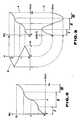
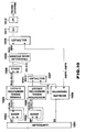
- Figure 1 shows the principle of the first embodiment.
- a carrier wave phase angle ⁇ ct sequentially increasing linearly between 0 and 2 ⁇ [rad] is made to be an address of a carrier wave ROM 101 to read carrier signal W c .
- Carrier wave phase angle ⁇ ct is obtained by multiplying time t[sec] by angular speed ⁇ c [rad/sec].
- "ct" is expressed as a group in a form of a suffix hereinafter if a specific reference is not made.
- a modulation wave phase angle ⁇ mt sequentially increasing linearly between 0 and 2 ⁇ [rad] is made to be an address of a modulation wave ROM 102 and a modulation signal read from modulation wave ROM 102 is multiplied by modulation depth function I(t)[rad], changing with time in a multiplier, hereinafter called MUL 103, to provide a modulation signal W M .
- This modulation wave phase angle ⁇ mt is obtained by multiplying angular speed ⁇ m [rad/sec] by time t [sec] and "mt" is expressed as a group and in a suffix form if a specific reference is not made.
- Modulation signal W M is added to carrier signal W C in adder (called ADD hereinafter) 104 and the added waveform W C + W M [rad] is further decoded by decoder 105 to provide a decoded output D.
- ADD adder
- Decoded output D is multiplied by amplitude coefficient A in MUL 106 to finally provide waveform output e.
- Carrier signal W C and modulation signal W M calculated in accordance with the above equations (3) and (4) are added and inputted to decoder 105, thereby causing output D to be outputted from decoder 105.
- Waveform output e obtained after the decoded output D is multiplied by amplitude coefficient A in MUL 106 is as follows.
- TRI(x) is defined as a triangular wave function.
- Carrier signal W C and carrier wave phase angle ⁇ ct are expressed by a relation A in Figure 3, based on equation (3) or Figure 2.
- modulation depth function I(t) in equation (5) is approaches 0 with time, thus realizing a process in which a musical sound is attenuated to a single sine waveform component or a musical sound comprising only a single sine waveform component.
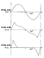
- waveform output e is gradually distorted from a single sine wave along the time axis, namely, waveform output e is varied to include a higher harmonics component along the frequency axis.
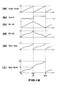
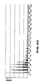
- Figure 5A to 5I show the frequency characteristics (power spectrum) of respective outputs e corresponding to Figures 4A to 4I.
- h1 shows a fundamental frequency (pitch frequency) and h2, h3, h4...show higher harmonics frequencies of two times, three times, four times...the fundamental frequency component.
- Figures 6A and 6B show histograms (occurrence number distributions) of the frequency characteristics of respective waveform outputs e composed under the same conditions using equation (5) of the present invention and equation (1) relating to an FM method of the prior art.
- the FM method shown in 6B cannot realize a harmonics component higher than the eleventh harmonics, but the present embodiment shown in Figure 6A is capable of realizing a higher harmonics component up to the thirtieth harmonics.
- the musical sound waveform generator shown in Figure 1 can generate a process in which the musical sound is attenuated to a single sine wave or a musical sound comprising only a single sine wave component similar to an actual musical sound, by changing the value of the frequency depth function I(t) from 0 to 2 ⁇ [rad].
- the musical sound waveform generator shown in Figure 1 can easily generate a musical sound in which a higher harmonics component clearly exists as a frequency component.
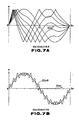
- the musical sound wavefrm generator of the present embodiment is particularly effective where a low-pitched musical sound is composed, namely, where a musical sound with a low fundamental frequency (pitch frequency) h1 and including plenty of higher harmonics within a range of linguistic frequency is composed.
- the waveform output e of Figure 7B is especially effective for producing higher harmonics produced by percussing a string, for example, an electric piano sound or vibraphone sound.
- a chorus effect is obtained by slightly shifting the ratio of ⁇ ct to ⁇ m from an integer ratio to a non-integer ratio (by performing a detune).
- a chorus effect can be similarly obtained by making the modulation wave phase angle ⁇ mt to be of a low frequency of about several hertz to several tens of hertz and by adding a phase modulation to the carrier wave phase angle ⁇ ct .
- a chime sound or drum sound including non-integer harmonics can be simulated by making the ratio of the carrier wave phase angle ⁇ ct to the modulation wave phase angle ⁇ mt to be a complete non-integer.
- a carrier wave ROM 101 stores a carrier signal W C which is represented by the equation (3), Figure 2 or the relation A shown in Figure 3.
- This carrier signal W C enables waveform output e of decoder 105 which has a characteristic shown by the equation (7) or a relation B shown in Figure 3 to be a sine wave, thereby producing a single sine wave.
- the present invention is not limited to the above situation and may enable decoder 105 to perform an arithmetic operation of a function originally including harmonics component other than a single sine wave and subsequently store in carrier wave ROM 101 a function for enabling the output D of the decoder 105 to be a sine wave, thereby achieving the same effect.
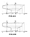
- Figures 8A to 8D show examples of combinations of a function to be arithmetically operated by decoder 105 and a function to be stored in carrier wave ROM 101.
- a function for enabling a carrier wave phase angle ⁇ ct to be associated with the carrier signal W C is stored in carrier wave ROM 101, and a function for enabling an input X to be associated with the decode output D is arithmetically operated by decoder 105.
- the characteristics correspoding to Figures 8A to 8D are explained hereinafter.
- single sine waves can be outputted as waveform output e from decoder 105 as a result of inputting carrier signal W C outputted from carrier wave ROM 101 as input x to decoder 105 where the value of modulation depth function I(t) in MUL 103 in Figure 1 is made to be 0.
- a waveform output e including a wide range of harmonics can be obtained depending on the functions of decoder 105 as shown in Figures 8A to 8D if the value of modulation depth function I(t) is made to be a value other than 0.
- the sine function is stored in modulation wave ROM 102 in Figure 1 and modulation is carried out by using modulation signal W M produced based on the equation (4).
- the present invention is not limited to the above case.
- a waveform including higher harmonics such as a tooth wave and a rectangular wave as shown in Figures 9A to 9C can be inputted to decoder 105 to thereby produce musical sound waveform including a wide range of higher harmonics.
- a logic circuit is provided inside the apparatus such that various phase angle waveform stored in ROM are input to the above logic circuit to thereby enable a modulation signal including higher harmonics.
- the structure of decoder 105 in Figure 1 for directly producing a waveform including high harmonics can be provided as an alternative to the above logic circuit to enable production of a modulation signal including higher harmonics.
- the amplitude coefficient A multiplied by MUL 106 in Figure 1 has been represented as a constant value in respective embodiments, but this amplitude coefficient A can actually be changed with time and thus the envelop characteristics subjected to amplitude modulation can be added to a musical sound.
- musical sound waveform generator of the present invention is applied to an electronic musical instrument.
- Figure 10 shows a view of an electronic musical instrument according to the first embodiment.
- the principle structure of the first embodiment in Figure 1 is used as a basis and thus Figure 1, for example, will be referred to in the following explanation.
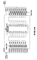
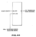
- Controller 1001 produces and outputs carrier frequency CF, modulator frequency MF and envelope data ED (respective rate values and level values, for example, of the envelope) in accordance with a setting state set by a parameter setting unit and a performance operation in a keyboard unit which are not shown in the drawing.
- Adders 1002 or 1004 feedback respective outputs therefrom to a terminal B where an input is added, and input carrier frequency CF or modulator frequency MF to adding terminal A so that 10 bit carrier wave phase angle ⁇ ct 0 to ⁇ ct 10 or modulation phase angle ⁇ mt 0 to ⁇ mt 10 whose value increase by the step width of respective frequencies is generated, thereby constituting an accumulator.
- Carrier wave phase angle ⁇ ct 0 to ⁇ ct 10 and modulation wave phase angle ⁇ mt 0 to ⁇ mt 10 respectively correspond to carrier wave phase angle ⁇ ct and modulation wave phase angle ⁇ mt in Figure 1.
- Carrier frequency CF corresponds to angular speed ⁇ C of carrier wave phase angle ⁇ ct
- modulator frequency MF corresponds to an angular speed ⁇ M of modulation wave phase angle ⁇ mt .
- carrier phase angle ⁇ ct 0 to ⁇ ct 10 and modulation wave phase angle ⁇ mt 0 to ⁇ mt 10 are respectively input to carrier signal generating circuit 1003 and modulation signal generating circuit 1005 as an address signal.
- Carrier signal generating circuit 1003 and modulation signal generating circuit 1005 respectively correspond to carrier wave ROM 101 and modulation wave ROM 102.
- envelop generator 1006 outputs modulation depth function I0 to I10 of two channels comprising 11 bits and 10 bits and amplitude coefficient AMP0-AMP10 from terminals C and N based on the envelop data ED obtained from controller 1001. These values respectively correspond to modulation depth function I(t) in Figure 1 and amplitude coefficient A, and can be changed with time.
- Modulation depth function I0-I10 has a value less than "1", is inputted to terminal B of multiplier 1007, and is multiplied with the output from modulation signal generating circuit 1005 inputted to terminal A, thereby producing modulation signal W M 0-W M 10 of 11 bits.
- Multiplier 1007 and modulation signal W M 0-W M 10 respectively correspond to MUL 103 and modulation signal W M in Figure 1.
- Carrier signal W C 0-W C 10 outputted from carrier signal generating circuit 1003 and modulation signal W M 0-W M 10 outputted from multiplier 1007 are respectively inputted to terminals A and B of adder 1008 for addition and output the adding waveform O0-O10 of 11 bit.
- Adder 1008 and adding waveform O0-O10 respectively correspond to ADD 104 and adding waveform W C +W M in Figure 1.
- Triangular wave decoder 1009 decodes outputs MA0-MA9 which respectively correspond to decoder 105 and decoded output D in Figure 1.
- Decoded outputs MA0-MA9 are further input to terminal A of multiplier 1010 and are multiplied with amplitude coefficients AMP0-AMP9 inputted to terminal B, thereby being amplitude-modulated.
- Amplitude coefficients AMP0-AMP1 show a value less than "1".
- the digital musical sound signal produced as recited above is converted to an analog musical sound signal in D/A converter 1011 and low pass filter 1012, so that the analog musical sound signal produces a sound through a sound system not shown in the drawing.
- carrier frequency CF, modulator frequency MF and envelop data ED are outputted from controller 1001 in accordance with a performance operation by a player, and a musical sound having a pitch, volume and tone controlled based on the performance operation is outputted as a sound in the same manner as in the musical waveform generator shown in Figure 1.
- Respective first input terminal of exclusive-logic-OR-circuit (called EOR hereinafter) #0 to #9 receive a carrier wave phase angle ⁇ ct 10 of the most significant bit from adder 1002 in Figure 10, and respective second input terminal thereof receive a carrier wave phase angle ⁇ ct 0- ⁇ ct 9 of 0-9 bits from adder 1002.
- the outputs A0-A9 from EOR 1102 of #0-#9 are input to the 1/2 wave carrier wave ROM 1101 as respective address signals.
- the ROM outputs D0-D9 from the 1/2 wave carrier wave ROM 1101 are input to the first input terminals of EOR 1103 of #0-#9.
- the carrier wave phase angle ⁇ ct 10 of the most significant bit is input to the second input terminals of EOR 1103 of #0-#9.
- Respective outputs of EOR 1103 of #0-#9 and carrier wave phase angle ⁇ ct 10 of the most significant bit are inputted to adder 1008 of Figure 10 as carrier signal W C 0-W C 10.
- a waveform corresponding to a 1/2 period ((0- ⁇ )rad) of carrier signal W C explained in Figure 2 or the equation (3) is stored in 1/2 wave carrier wave ROM 1101 in Figure 11.
- the value determined by outputs D0-D9 of the 1/2 wave carrier wave ROM 1101 in Figure 11 based on the equation (3) is expressed as Y1 and then the following waveform is stored.
- a carrier wave phase angle ⁇ ct means the value determined by ⁇ ct 0- ⁇ ct 9.
- carrier wave phase angle ⁇ ct 0- ⁇ ct 10 outputted from adder 1002 in Figure 10 can designate phase angles 0- ⁇ [rad] in a full range of the lower 10 bits corresponding to ⁇ ct 0- ⁇ ct 9, in which the most significant bit ⁇ ct 10 is in logic "0". Further, a phase angle of ⁇ -2 ⁇ [rad] can be designated in a full range of ⁇ ct 0- ⁇ ct 9, in which ⁇ ct 10 is in logic "1".
- carrier wave phase angle ⁇ ct 10 of the most significant bit is logic 0 as shown in Figure 12B and a full range of the lower 10 bits corresponding to carrier wave phase angle ⁇ ct 0- ⁇ ct 9 is designated.
- carrier wave phase angle ⁇ ct 10 is inputted to the first input terminals EOR 1102 of #0-#9, and when the value of the lower 10 bits corresponding to carrier wave phase angle ⁇ ct 0- ⁇ ct 9 sequentially increases in the period 0-T/2, address signals A0-A9 which sequentially increases in the same manner as the carrier wave phase angle increases are obtained. Therefore, the outputs D0-D9 in a range from 0- ⁇ [rad] based on the equation (17) are sequentially read out from 1/2 wave carrier wave ROM 1101 in Figure 11.
- the waveform is input to the first input terminals of EOR 1103 of #0-#9 and the most significant bit with a logic "0" corresponding to carrier phase angle ⁇ ct 10 is input to the second intput terminal of EOR 1103 and thus, carrier signal W C 0-W C 9 of the lower 10 bits of the output of EOR 1103 are, as shown in Figure 12E, the same waveform as the outputs D0-D9 of Figure 12D. Further, as carrier signal W C 10 of the most significant bit is equal to carrier wave phase angle ⁇ ct 10 of the most significant bit with a logic "0", the same waveform as output D0-D9 shown in Figure 12D is outputted as carrier signal W C 0-W C 10, as shown in the period 0 to T/2 in Figure 12(f).
- carrier wave phase angle ⁇ C 10 of the most significant bit is logic "1" as shown in Figure 12(b), and a full range of carrier wave phase angle ⁇ ct 0- ⁇ ct 9 of the lower 10 bits is designated.
- carrier wave phase angle ⁇ ct 10 of the most significant bit of the logic "1" is input to the first input terminals of EOR 1102 of #0-#9, and when the value of carrier wave phase angle ⁇ ct 0 to ⁇ ct 9 of lower 10 bits sequentially increases in the period T/2 to T, address signals A0-A9 sequentially decreasing in an opposite manner as shown in Figure 12(c).
- a waveform in a range from 0 to ⁇ [rad] based on the equation (17) is read out in an opposite direction as shown in Figure 12(d) to provide outputs D0-D9 from 1/2 wave carrier wave ROM 1101 in Figure 11.
- the waveform is input to the first input terminals of EOR 1103 of #0-#9 and, as carrier wave phase angle ⁇ ct 10 of the most significant bit of the logic "1" is input to the second input terminal of EOR 1103, as shown in Figure 12(e), carrier signals W c 0-W c 9 of the lower 10 bits of the output of EOR 1103 is outputted to provide a waveform increasing and decreasing in a manner opposite to the outputs D0-D9 shown in Figure 12(d).
- carrier signal W C 10 of the most significant bit is equal to carrier wave phase angle ⁇ ct 10 of the most significant bit with a value of logic "1" and thus, an offset of ⁇ [rad] corresponding to a full range of carrier wave phase angle ⁇ ct 0- ⁇ ct 9 of the lower 10 bits is superimposed to the above output.
- the waveform shown in the period T/2 - T of Figure 12(f) is outputted as carrier signal W C 0-W C 10.
- the waveform output in the period from 0 to T is the same as the waveform of carrier signal W C explained above by referring to Figure 2 and the equation (3).
- a waveform with a 1/2 period only has to be stored in 1/2 wave carrier wave ROM 1101 shown in Figure 11, that is, in comparison with the waveform with one period shown in Figure 2. Therefore, the capacity of the memory can be simply made 1/2 as compared with the case in which a waveform with a period of 1 is stored.
- Figure 13 shows the structure of the second circuit example of carrier signal generating circuit 1003 of Figure 10.
- Carrier wave phase angle ⁇ ct 9 of the 10th bit from adder 1002 in Figure 10 is inputted to respective first input terminals #0-#8 of EOR 1302 and carrier wave phase angles ⁇ ct 0- ⁇ ct 8 of 0 to 8 bits are inputted to the respective second input terminals.
- Outputs A0-A8 of EOR 1302 of #0-#8 are input to 1/4 wave carrier wave ROM 1301 as respective address signals.
- ROM outputs D0-D8 from 1/4 wave carrier wave ROM 1301 are inputted to the first input terminals of EOR 1303 of #0-#8.
- Carrier wave phase angle ⁇ ct 9 of the 10th bit is inputted to second input terminals of EOR 1303 of #0-#8.
- Respective outputs of EOR 1103 of #0-#8, carrier wave phase angle ⁇ ct 9 of the 10th bit and carrier wave phase angle ⁇ ct 10 of the most significant bit are outputted to adder 1008 in Figure 10 as carrier signal W c 0-W c 10.
- the operation of the second circuit example is expalined by referring to an operation explanatory view.
- a wave corresponding to 1/4 period (0- ⁇ /2[rad]) of carrier signal W C explained by referring to Figure 2 or the equation (3) is stored in 1/4 wave carrier wave ROM 1301 in Figure 13. Supposing that the value determined by the outputs D0-D8 from 1/4 wave carrier wave ROM 1301 in Figure 13 in accordance with equation (3) is Y2, then the following waveform is stored.
- the carrier phase angle ⁇ ct means the values determined by ⁇ ct 0- ⁇ ct 8.
- phase angle ⁇ ct 0 to ⁇ ct 10 outputted from adder 1002 in Figure 10, where a combination ( ⁇ ct 10, ⁇ ct 9) of a logic of most significant bit ⁇ ct 10 and 10th bit ⁇ ct 9 is (0, 0), a phase angle of 0 to ⁇ /2 [rad] can be designated by a full range of the lower 9 bits of ⁇ ct 0- ⁇ ct 8. Where the combination becomes (0, 1), a phase angle of ⁇ /2 - ⁇ [rad] can be designated by a full range of the lower 9 bits ⁇ ct 0 - ⁇ ct 8.
- T A period in which a full range of carrier wave phase angle ⁇ ct 0- ⁇ ct 10 is designated by adder 1002 of Figure 10 is shown by T.
- carrier wave phase angle ⁇ ct 9 of the 10th bit of the logic "0" is input to the first input terminals of EOR 1302 of #0-#8 and the value of carrier phase angle ⁇ ct 0- ⁇ ct 8 of the lower 9 bits sequentially increase in the period 0-T/4.
- carrier signal W C 10 of the 10th bit and W C 9 of the most significant bit are equal to the carrier wave phase angle ⁇ ct 9 of the 10th bit and ⁇ ct 10 of the most significant bit respectively and are commonly logic "0".
- carrier signal W C 0-W C 10 is outputted as carrier signal W C 0-W C 10.
- the outputs D0-D8 of 1/4 wave carrier wave ROM 1301 in Figure 13 can be read in a reverse direction to provide a waveform in a range from 0 to ⁇ /2 [rad] based on the equation (18).
- the waveform is inputted to the first input terminals of EOR 1303 of #0-#8, and carrier wave phase angle ⁇ ct 9 of the 10th bit of the logic "1" is input to the second input terminals of EOR 1303.
- carrier signals W C 0-W C 8 of the lower 9 bits outputted from EOR 1303 are, as shown in Figure 14(f), waveforms which increase and decrease in a manner opposite to the outputs D0-D8 shown in Figure 14(e).
- carrier signal W C 9 of the 10th bit and carrier signal W C 10 of the most significant bit are respectively equal to the carrier wave phase angle ⁇ ct 9 of the 10th bit and carrier wave phase angle ⁇ ct 10 of the most significant bit and are respectively logic "1" and "0". Therefore, an offset of ⁇ /2 [rad] corresponding to a full range component of carrier wave phase angles ⁇ ct 0- ⁇ ct 9 of the lower 10 bit is added to the above output. As a result, the waveform shown in the period T/4-T/2 in Figure 14(g) is outputted as a carrier signals W C 0-W C 10.
- carrier signal W C 9 of the 10th bit and carrier signal W C 10 of the most significant bit are respectively equal to carrier wave phase angle ⁇ ct 9 of the 10th bit and carrier wave phase angle ⁇ ct 10 of the most significant bit with respective logic value of "0" and "1". Therefore, an offset of ⁇ [rad] corresponding to twice the full range of carrier wave phase angle ⁇ ct 0- ⁇ ct 8 of the lower 9 bits is added to the above output and as a result, a waveform shown in a period T/4-T/2 in Figure 14 (g) is outputted as carrier signals WC0-WC10.
- carrier signal W C 9 of the 10th bit and carrier signal W C 10 of the most significant bit are respectively equal to carrier phase angle ⁇ ct 9 of the 10th bit and carrier wave phase angle ⁇ ct 10 of the most significant bit with a common logic value of "1".
- An offset of 3 ⁇ /2 corresponding to three times the full range of carrier wave phase angle ⁇ ct 0- ⁇ ct 8 of the lower 9 bits is added to the above outputs and as a result, a waveform designated during the period of 3T/4 as shown in Figure 14(g) is outputted as carrier signals W C 0-W C 10.
- the waveform outputted during the period 0-T is the same waveform as that of carrier signal W C as explained referring to Figure 2 or the equation (3).
- a 1/4 period of a waveform may be stored in 1/4 wave carrier wave ROM 1301 of Figure 13 with regard to a waveform of a single period shown in Figure 2.
- the memory capacity can be made 1/2 as compared with the first circuit example and is merely made 1/4 as compared with the case where a waveform of one period stored.
- Figure 1 5 shows a circuit example of triangular wave decoder 1009 of Figure 10.
- the addition waveform O9 of the 10th bit and the addition waveform O10 of the most significant bit from adder 1008 in Figure 10 are inputted to respective input terminals of #9. This output is inputted to the respective first terminals of EOR 1501 of #0-#8.
- Addition waveform O0 to O8 of 0 to 8 bit are inputted to the respective second terminals of EOR 1501 of #0-#8.
- Respective outputs of EOR 1501 of #0-#8 are inputted to a multiplier 1010 in Figure 10 as the decoded outputs MA0-MA8, and addition waveform O10 of the most significant bit are inputted to the multiplier 1010 as the decoded output MA9.
- triangular wave decoder 1009 operates in the same manner as decoder 105 in Figure 1 represented by the characteristic of the equation (7) as shown in Figure 15.
- Modulation signal generating circuit 1005 of Figure 10 can be realized by ROM memory for storing a sine wave of 1/2 or 1/4 the period of generating a waveform of one period in a manner similar to Figure 11 or 13.
- Adders 1002, 1005 and 1008, or multipliers 1007 and 1010 can be realized by a well-known circuit, and envelope generator 1006 can be realized by a well-known circuit in the electronic musical instrument field.
- the first embodiment of Figure 10 has been identified as a circuit for outputting a single musical sound waveform.
- adder 1002, carrier signal generating circuit 1003, adder 1004, modulation signal generating circuit 1005, envelop generator 1006, multiplier 1007, adder 1008, triangular wave decoder 1009 and multiplier 1010 are constructed in a manner such as they can operate in a time divisional manner.
- envelop generator 1006, multiplier 1007, adder 1008, triangular wave decoder 1009 and multiplier 1010 are constructed in a manner such as they can operate in a time divisional manner.
- a musical sound of respective time divisional channels is accumulated every sampling period at an input stage of D/A converter 1011.
- a plurality of musical sound waveforms can therefore be produced in parallel.
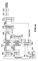
- FIG 16. This embodiment is an example in which a musical sound waveform generator of the present invention is applied to an electronic keyboard.
- the present embodiment is characterized by controlling a wide change in state from higher harmonics in a produced musical sound to a single sine wave in a produced musical sound based on the speed (strength) of depression of a key on a keyboard of a musical instrument.
- the circuit or signals given the same number as the symbol as in the first embodiment in Figure 10 perform the same function as in Figure 10.
- the second embodiment of Figure 16 is different from the first embodiment in Figure 10 in that keyboard unit 1601 is connected to controller 1602 (which corresponds to a controller 1001 in Figure 10).
- Controller 1602 produces an output carrier frequency CF, modulator frequency MF and envelope data ED and FA (which will be explained in detail later), depending on the state of a parameter set by a setting unit not shown in the drawing, and depending on a key code KC and a velocity VL from keyboard 1601.
- Adders 1002 or 1004 are accumulators for respectively generating carrier wave phase angle ⁇ ct 0- ⁇ ct 10 of 10 bits or modulation wave phase angle ⁇ mt 0- ⁇ mt 10 in the same manner as in Figure 10.
- Carrier frequency CF is determined to be a frequency corresponding to a key code KC from keyboard unit 1601, for example, and modulator frequency MF is determined to provide the ratio previously set by a performer with regard to a carrier frequency CF, for example, thereby generating a musical sound waveform of a pitch corresponding to the keyboard operation of the performer.
- carrier signal generating circuit 1003 and modulation signal generating circuit 1005 The function of carrier signal generating circuit 1003 and modulation signal generating circuit 1005 is the same as in Figure 10.
- envelope generator 1603 outputs modulation depth function I0-I10 of two channels comprising 11 bits and 10 bits, respectively, and further outputs amplitude coefficients AMP0-AMP10 from terminals C and M of controller 1602 based on the address data FA and setting data ED from controller 1602. These correspond to modulation depth function I(t) and amplitude coefficient A in Figure 1, and can be changed with time based on key codes KC and velocity VL inputted from keyboard unit 1601. This feature differs from the first embodiment shown in Figure 10.
- the functions and operation of multiplier 1007, adder 1008, triangular wave decoder 1009, multiplier 1010, D/A converter 1011 and low pass filter 1012 are all the same as in the first embodiment shown in Figure 10.
- carrier signal generating circuit 1003 in Figure 16 is the same as that in Figures 11 and 13 of the first embodiment. Operation has already been explained with reference to Figures 12 and 14.
- triangular wave decoder 1009 in Figure 16 is the same as that in Figure 15 of the first embodiment. Operation has also already been explained.
- modulation signal generating circuit 1005 in Figure 16 can be realized as the circuit for storing 1/2 or 1/4 period of sine waveform in ROM and for generating a waveform of one period in the same manner as in Figures 11 and 13.
- an envelope generator 1603 in Figure 16 is the same as that of the envelope generator circuit used in an ordinary electronic musical instrument, except that an envelope waveform for two channels can be outputted in the case of the present invention.
- the present embodiment has characteristics in that respective parameters are set in envelope generator 1603 from controller 1602. The operation will be explained below.
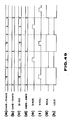
- modulation depth function I0-I10 and amplitude coefficients AMP0-AMP9 respectively outputted as channel Ch1 and Ch2 from, envelope generator 1603 are shown in Figure 17.
- ON designates a timing means when a key on keyboard unit 1601 in Figure 16 is depressed
- OFF designated a timing means when a key depression is released.
- Respective output values of channel Ch1 and channel Ch2 reaches an initial level IL during the period of an attack time AT starting with the depression of the key and becomes a sustain level SL when decay time DT elapse from the time of initial level IL.
- the sustain level SL is maintained until the key is released and the level becomes 0 in a release time RT after a release of the key, thereby enabling the sound to be silent.
- Address data FA is set to the address input terminal A of envelope generator 1603 by controller 1602 in Figure 16 and the setting data ED is provided to data input terminal D, thereby enabling respective output waveforms channel Ch1 and channel Ch2 of envelope generator 1603 in Figure 16 to be set.
- the relation between the address value of address input terminal A and the kind of data of data input terminal D is shown in Figure 18.
- various kinds of data shown in Figure 18 can be set to data input terminal D by setting data ED.
- the same kind of parameter is set in channel Ch1 and Ch2 in figure 18, but the kind of the parameter may be different.
- controller 1602 an operational flowchart of controller 1602 is shown in Figures 19 to 25 when a performer plays by operating keyboard unit 1601 shown in Figure 16. Respective variable numbers to be processed by controller 1602 are shown in Figure 26.
- Detune data DTUNE of a modulation wave with regard to a carrier wave in Figure 26 designates how much the frequency of modulation wave phase angle ⁇ mt 0- ⁇ mt 10 is shifted from the frequency of carrier wave phase angle ⁇ ct 0- ⁇ ct 10 upon setting the frequency, thereby varying the structure of the higher harmonics of a musical waveform produced.
- Respective data corresponding to channel Ch1 and channel Ch2 in Figure 26 correspond to respective data shown in Figure 18 and set in envelope generator 1603 of Figure 16.
- FIG 19 is the main operational flowchart of controller 1602. In a repetition of processes from S1 to S7 in Figure 19, controller 1602 watches which key is depressed or released on keyboard unit 1601.
- key code KC is obtained by a depression from keyboard unit 1601.
- values such as vendor and transpose which are not shown in Figure 20 are added to key code KC to calculate carrier frequency CF.
- the vendor value is the data of the controller provided so that the performer can discretionally change the pitch of a musical sound which is being produced during the performance.
- the transpose value is the setting data for shifting of the key or changing of an octave upon keyboard unit 1601.
- detune data DTUNE (which should be referred to Figure 26) is set beforehand by a performer and is added to the carrier frequency CF set in S2 ( Figure 20), thereby calculating the modulator frequency MF.
- Modulator frequency MF determined as recited above, is outputted to adder 1004. Therefore, adder 1004 outputs modulation wave phase angle ⁇ mt 0- ⁇ mt 10 having a predetermined relationship with carrier wave phase angle ⁇ ct 0- ⁇ ct 10 outputted from adder 1002 in Figrue 16.
- velocity VL of a key depressed on keyboard 1601 in Figure 16 can be obtained.
- the value can be obtained between 0 to 1.
- attack time MAT decay time MDT and release time MRT of channel Ch1 (which should be referred to Figure 26) is set in envelope generator 1603 in Figure 16 as tone data.
- This setting is conducted by determining the value provided to address input terminal A of envelope generator 1603 by address data FA and by outputting the corresponding various variable value to data input terminal D as setting data ED as shown in Figure 18.
- the initial level MIL of channel ch1 which is tone data, is multiplied by a value of velocity VL and is set in envelope generator 1603.
- the setting operation is conducted in the same manner as at S15.
- sustain level MSL of channel Ch1 which is tone data, is multiplied by velocity VL and then is set in envelope generator 1603 in the same manner as above.
- attack time CAT initial level CIL
- decay time CDT decay time CDT
- sustain level CSL release time CRT (which should be referred to Figure 26) of channel Ch2 are set in envelope generator 1603 in Figure 16 as tone data.
- the setting operation is conducted in the same manner as in channel Ch1.
- a command for turning on channel Ch1 is provided to envelope generator 1603, as shown in Figure 16. This process is executed by enabling controller 1602 of Figure 16 to set the value 0 at address data FA and to output an appropriate command data as setting data ED.
- a command for turning on channel Ch2 is provided to envelope generator 1603. This process is executed by enabling controller 1602 of Figure 16 to set the value 7 as an address data FA, and to output an appropriate command data as setting data ED, as shown in Figure 18, in the same manner as in channel ch1.
- a command for turning on channel Ch1 is provided to envelope generator 1603 in Figure 16. This process is executed by enabling controller 1602 of Figure 16 to set the value 1 as address data FA, and outputs an appropriate command data as setting data ED, as shown in Figure 18.
- a command for turning off channel Ch2 is provided to envelope generator 1603. This process is executed by enabling controller 1602 in Figure 16 to set the value 8 as address data FA and to output an appropriate command data as setting data ED, as shown in Figure 18 in the same manner as in channel ch1.
- modulation depth function I0-I10 and amplitude coefficient AMP0-AMP9 corresponding to channel ch1 are produced from envelope generator 1603 in Figure 16 with such characteristics as shown in Figure 17. Based on these data, respective circuit in Figure 16 are operated as explained above to generate a musical sound waveform.
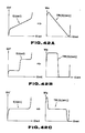
- a characteristic of modulation depth function I0-I10 corresponding to channel Ch1 varies as shown in Figure 27 in accordance with the value of velocity VL representing the strength of a depressed key on keyboard unit 1601 in Figure 16.
- the present embodiment has a feature of controlling a wide change in state from higher harmonics in the produced musical sound to a single sine wave in the produced musical sound, based on the strength or speed of the depression of the key.
- the envelope characteristics of channel Ch1 of envelope generator 1603 in Figure 16 namely, the modulation depth functions I0-I10, can be changed in accordance with a velocity VL and envelope characteristics of channel Ch2.
- the amplitude coefficient AMP0-AMP9 can be changed by velocity VL, thereby varying the sound volume of the musical sound in accordance with the strength of the depression of a key.
- modulation depth function I0-I10 is changed by velocity VL and is controlled by the key of keyboard unit 1601 in Figure 16 which is depressed. Namely, where a key of a lower range is depressed, the value of modulation depth functions I0-I10 is made small and, where the key in a higher range is depressed, it is made large, thereby enabling suitable operation for simulation of a tone including higher harmonics in a lower range such as a piano sound.
- the embodiment of Figure 16 has been identified as a circuit outputting a single musical sound waveform.
- adder 1002, carrier signal generating circuit 1003, adder 1004, modulation signal generating circuit 1005, envelope generator 1603, multiplier 1007, adder 1008, triangular wave decoder 1009 and multiplier 1010 in Figure 16 may be constructed to be operated in a time divisional manner.
- a musical sound of respective time divisional channels is accumulated every sampling period at an input stage of D/A converter 1011.
- a plurality of musical sound waveforms can therefore be produced in parallel.
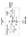
- Figure 28 shows this principle strucure of a basic module 2801.
- the basic module is different from the principle structure of the first embodiment shown in figure 1. Namely, modulation signal W M is not input to through MUL 103 from modulation wave ROM 102 unlike case where the basic module receives the output of the previous basic module as is described later. However, the basic operation per module is almost the same as in Figure 1.
- Carrier signal W C arithmetically operated in accordance with the equation (3) and modulation signal W M transmitted from an external unit are added and are inputted to decoder 105.
- the decoded output D is outputted from decoder 105 and further multiplied by amplitude coefficient A in MUL106, thereby providing the following wavefrom output e.
- TRI(x) is defined as a rectangular function.
- modulation signal W M inputted from an external unit is made close to 0 with time in order to realize a process in which a musical sound is attenuated to comprise only a single sine wave component. Or the modulation signal is 0 to generate musical sound comprising only a single sine wave component.
- carrier wave ROM 101 stores carrier signal W C represented by the equation (3) or relation A of Figures 2 or 3 and enables waveform output e of decoder 105 to comprise a sine wave, the decoder 105 having characteristics shown by the equation (7) or relation B of Figure 3, thereby enabling a single sine wave to be produced.
- the present invention is not limited to the above case and a combination shown in Figures 8A to 8D may provide the same effect as in the case shown in Figure 1. These relations are shown by the above recited equations (9) to (16).
- amplitude coefficient A multiplied by MUL 106 is identified as a constant value but it can actually be changed with time as in the case shown in Figure 1.
- the amplitude modulated envelope characteristic can be added to waveform output e.
- Figure 29 is a structural view of an entire electronic musical instrument according to the third embodiment.
- the present embodiment comprises a structure of the basic module shown in Figure 28 as a basis and thus the present embodiment is explained by referring to Figure 28 when necessary.
- Controller 2906 produces carrier wave phase angle ⁇ ct 0- ⁇ ct 10 comprising 11 bits, amplitude coefficients AMP0-AMO9 comprising 10 bits, formation data F0, F1, F2 and F3, two phase clock CK1 and CK2, and latch clock ECLK in accordance with the state of parameters set by setting unit (not shown and described leter) and a pitch designation operation performed by, for example, a keyboard unit.
- setting unit not shown and described leter
- a pitch designation operation performed by, for example, a keyboard unit.
- repsective data corresponding to the number of the basic module which are combined per formation is outputted in a time divisional manner. This is described later in detail.
- Carrier phase angle ⁇ ct 0- ⁇ ct 10 and amplitude coefficients AMP0-AMP9 correspond to carrier wave phase angle ⁇ ct and amplitude coefficient A in Figure 28.
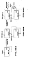
- Basic module 2901 corresponds to basic module 2801 in Figure 28 and is constituted by carrier signal generating circuit 2902 corresponding to carrier wave ROM 101 shown in Figure 28, triangular wave decoder 2904 corresponding to decoder 105, adder 2903 corresponding to ADD 104 and multiplier 2905 corresponding to MUL 106.
- Carrier wave phase angle ⁇ ct 0- ⁇ ct 10 and amplitude coefficients AMP0-AMP9 are respectively supplied to carrier wave generating circuit 2902 and multiplier 2905 from controller 2906.
- carrier signals W C 0-W C 10 comprising 11 bits outputted from carrier signal generating circuit 2902 correspond to carrier signal W C in Figure 28.
- Addition waveforms O0-O10 comprising 11 bits outputted from adder 2903 correspond to addition waveform W C +W M in Figure 28.
- Decoded outputs MA0-MA9 comprising 10 bits outputted from trianglular wave decoder 2904 correspond to decoded output D in Figure 28.
- Waveform outputs e0-e10 comprising 11 bits outputted from multiplier 2905 corresponds to waveform output e in Figure 28.
- Waveform output e0-e10 outputted from basic module 2901 is selectively outputted to accumulator 2908 or 2907 through switch SW2913, which is controlled to be connected to terminal S0 or S1 depending on a logic "0" or logic "1" of formation data F0 outputted from controller 2906.
- Accumulator 2907 accumulates waveform outputs e0-e10 from basic module 2901 after receiving the waveform outputs e0-e10 from terminal S1 of switch SW2913. This process is controlled by formation data F2 inputted to clear terminal CLR of accumulator 2907 from controller 2906, and two phase clock CK1 and CK2 transmitted from controller 2906. The structure will explained later by referring to Figure 30.
- the output of accumulator 2907 is applied to terminal S1 of swtich SW2914; terminal S0 of swtich SW2914 is fixed to level logic "0".
- Switch SW2914 connects terminal S0 or S1 to adder 2903 of basic module 2901 depending on whether formation data F3 from controller 2901 is logic "0" or logic "1", thereby supplying modulation signals W M 0-W M 10 of 11 bits.
- Terminal S0 of switch SW2914 is not limited to the logic "0" level and may be a value near "0" as long as it does not effect the modulation of the carrier signal.
- accumulator 2908 accumulates waveform outputs e0-e10 of basic module 2901 after receiving the waveform output from terminal S0 of switch SW2913. This process is controlled by formation data F1 inputted to clear terminal CLR from controller 2906, and two phase clock CLK1 and CLK2 from controller 2906. The structure will be explained in detail by referring to Figure 31.
- the output of accumulator 2908 is latched at a flip-flop (which is called F/F hereinafter) in accordance with latch clock ECLK from controller 2906, thereby providing a digital musical sound signal.
- the digital musical sound signal formed as stated above is converted into an analog musical sound signal in D/A converter 2910 and low-pass filter (LPF) 2911, and produces a sound through sound system 2912.
- D/A converter 2910 and low-pass filter (LPF) 2911 low-pass filter
- FIG. 11 A detailed circuit example of carrier signal generating cricuit 2902 of basic module 2901 in Figure 29 is shown in figures 11 or 13 in a manner similar to the first embodiment, and their operations are performed in the same manner as explained in Figure 12 or 14.
- FIG. 15 A detailed circuit example of a triangular decoder 2904 in Figure 29 is shown in figure 15 in the same manner as in the first embodiment and the operation is performed in the same manner previously explained.
- Figure 30 shows a circuit structure of accumulator 2907 of Figure 29. Waveform outputs e0-e10 of 11 bits from basic module 2901 through terminal S1 of switch SW 2913 in Figure 29 are inputted to addition input terminal IA of adder 3001 through input terminal IN, and are added to inputs of 11 bits supplied from AND circuits 3003-1 - 3003-10 connected to addend input terminal IB.
- the outputs of 11 bits from the addition output terminal A+B of adder 3001 are set to F/F 3002 at a timing when clock CLK1 is outputted from controller 2906 in Figure 29.
- the above data set to F/F 3002 is read at a timing when clock CK2 outputted from controller 2906 in Figure 29 rises, is outputted to terminal S1 of switch SW2914 in Figure 29 from output terminal OUT, and is selectively accumulated by being fed back to addend input terminal IB of adder 3001 through AND circuit 3003-1 - 3003-10.
- Formation information data F2 from controller 2906 in Figure 29 is inputted to AND circuit 3003-1 - 3003-10 after it is inverted by inverter 3004, thereby performing an opening and closing operation of the AND circuit.
- Waveform outputs e0-e10 comprising 11 bits outputted from basic module 2901 is received by accumulator 2908 through terminal S0 of switch SW2913 in Figure 29 and is inputted to addition input terminal IA of adder 3101 from input terminal IN.
- the structure of adder 3101, F/F 3102, and circuits 3103-1 - 3103-10 and inverter 3104 is the same as that of accumulator 2907 in Figure 31.
- Figure 29 An entire operation of the electronic musical instrument shown in Figure 29 is explained. This explanation mainly concerns variations between the basic module 2901 and acumulators 2097 and 2908 and switches SW2913, SW2914 and F/F2909.
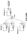
- Figures 33A to 33G show an example of the formation of an electronic musical instrument according to the third embodiment. This formation can be selected by a player through a parameter setting unit, not shown. By this means, a player can control the production of a musical sound comprising various harmonics structures.
- M1 to M4 in Figures 33A to 33G show an arithemetic operation unit executed by basic module 2901 in Figure 29. Respective process periods are obtained by dividing a sampling period into 4 process periods (called M1 process period - M4 process period) in a time divisional manner.
- formation data F0-F3, clocks CK1, CK2 and latch clock ECLK are abbreviated as F0-F3, CK1, CK2 and ECLK.
- a timing t1 (hereinafter called t1 and t2-t8 are used in a similar manner) in which CK2 is logic "1" during M1 process, F3 is logic "0" and the value 0 is supplied as modulation signals W M 0-W M 10.
- waveform outputs e0-e10 from basic module 2901 is a single frequency sine wave multiplied by amplitude coefficients AMP0-AMP9. This output is expressed as e(M1).
- F0 becomes logic "1" at t1, as shown in Figure 32A, the above e(M1) is inputted to accumulator 2907.
- F2 is logic "1" at t1 as shown in Figure 32A, i.e., AND circuits 3001-1 - 3001-10 are turned off. All 0 is inputted to addend input terminal IB and e(M1) is outputted from addition output terminal A+B of adder 3001. e(M1) is set in F/F 3002 at t2 at which CK1 is logic "1".
- F1 is logic "1" as shown in Figure 32A and thus AND circuits 3103-1 - 3103-10 are turned off and all 0 is inputted to addend input terminal IB and addition output terminal A+B of adder 3101 outputs e(M4) at output terminal OUT.
- the e(M4) is latched at F/F 2909 in Figure 29 at t8 at which ECLK is logic "1".
- basic module 2901 of Figure 29 outputs one sample of musical waveform e(M4) modulated in three serial stages of M2-M4 process periods and by repeating the above operation, sound system 2912 produces a musical sound through D/A converter 2910 and LPF 2911.
- e(M3) is inputted to accumulator 2908 and F1 simultaneously becomes logic "1" and addend input terminal IB of adder 3101 in Figure 31 receives an all 0 signals and addition output terminal A+B of adder 3101 outputs e(M3).
- This e(M3) is set to F/F 3102 at t6 at which CK1 becomes logic "1".
- basic module 2901 in Figure 29 adds waveform output e(M3) modulated in a serial two stages of M2 and M3 process periods to sine wave e(M4) formed during M4 process period, thereby outputting one sample of an added musical sound waveform.
- sound system 2912 produces the corresponding modulated musical sound through D/A converter 2910 and LPF 2911.
- addition output terminal A+B of adder 3001 produces e(M1) and at t2, at which CK1 becomes logic "1", it is set to F/F 3002.
- the opearation during the M2 process period is the same as that during the M2 process period in the example of the formation in Figure 33A. Namely, at t3, at which CK2 becomes logic "1", output terminal OUT of accumulator 2907 in Figure 30 outputs e(M1) and F3 simultaneously becomes logic "1” thereby enabling basic module 2901 in Figure 29 to output waveform output e(M2) and to be modulated based on e(M1) at t3.
- F0 becomes logic "0” and then, as in the M4 process period in the example of the formation in Figure 33A, e(M2) is inputted to accumulator 2908.
- F1 simultaneously becomes logic "1” and addend input terminal IB of adder 3101 in Figure 31 receives a all 0 signals, thereby enabling addition output terminal A+B of adder 3101 to produce e(M2).
- This e(M2) is set to F/F 3102 at t4, at which CK1 becomes logic "1".
- AND circuits 3103-1 - 3103-10 are turned on and e(M2) is received by addend input terminal IB and output terminal OUT from addition output terminal A+B of adder 3101 outputs e(M2) + e(M4). Therefore, e(M2)+e(M4) is latched at F/F 2902 of Figure 29 at t8 at which DCLK becomes logic "1".
- one output sample of a musical sound waveform is obtained by adding waveform output e(M2).
- This sample is modulated by basic module 2901 in Figure 29 during the M2 process period and waveform output e(M4) is modulated during the M4 process period.
- sound system 2912 produces the corresponding modulated musical sound through D/A converter 2910 and LPF 2911.
- a musical sound waveform is obtained by mixing two kinds of modulated components.
- F1 simultaneously becomes logic "0", as shown in Figure 32D, circuits 3103-1 - 3101-10 are turned on, addend input terminal IB receives the above e(M1) and addition output terminal A+B of adder 3101 outputs e(M1)+e(M2) from the output terminal.
- CK1 becomes logic "1"
- F1 is logic "0” and AND circuits 3103-1 - 3103-10 are turned on, thereby enabling e(M1)+e(M2) to be inputted to addend input terminal IB and output terminal OUT from addition output terminal A+B of adder 3101 outputs e(M1 )+e(M2 )+e(M3).
- t6 when CK1 becomes logic "1", it is set to F/F3101.
- F1 is logic "0" and AND circuit 3103-1 - 3103-10 are turned on.
- addend input terminal IB receives e(M1)+e(M2)+e(M3) and addition output terminal A+B of adder 3101 outputs e(M1)+e(M2)+e(M3)+e(M4) at the output terminal OUT.
- This output is latched at F/F2902 of Figure 29 at t8 at which ECLK becomes logic "1".
- a musical sound waveform by a sine wave composition method is provided in which four kinds of sine wave component are mixed.
- the operational sequence of the M3 process period is the same as that of the M2 process period. Namely, at t5, at which CK2 becomes logic "1", F3 becomes logic "0" and basic module 2901 in Figure 29 outputs waveform output e(M3) comprising non-modulated single sine wave. Simultaneously, at t5, as shown in Figure 32E, F0 is logic "0" and e(M1) is inputted to accumulator 2907. Accumulator 2907 in Figure 30 outputs from output terminal, e(M1)+e(M2) set in F/F3002 at t5 at which CK2 becomes logic "1".
- F2 is logic "0"
- AND circuits 3003-1 - 3003-10 are turned on
- addend input terminal IB receives the above e(M1)+e(M2)
- addition output terminal A+B of adder 3001 outputs e(M1)+e(M2)+e(M3) and at t6, at which CK1 becomes logic 1, it is set to F/F3002.
- AND circuits 3103-1 - 3103-10 are turned off and addend input terminal IB receives all 0 signals and addition output terminal A+B of adder 3101 outputs e(M4) at output terminal OUT.
- e(M4) is latched by F/F2909 in Figure 29.
- basic module 2901 outputs one sample of musical waveform e(M4) modulated by a waveform comprising a mixture of three kinds of sine waves obtained during the M1 to M3 process period.
- sound system 2912 produces a corresponding modulated musical sound through D/A converter 2910 and LPF 2911.
- e(M1) is sequentially outputted at output terminal OUT of accumulator 2907 of Figure 30.
- F3 simultaneously becomes logic "1” and basic module 2901 of Figure 29 outputs waveform output e(M3) modulated based on e(M1).
- F0 is logic "0”.
- e(M3) is inputted to accumulator 2908.
- accumulator 2908 shown in Figure 31 at t5, CK2 becomes logic "1", and e(M2) is set to F/F3102 and outputted to FFOUT.
- the operation of the M1 process period is similar to that of the M1 process period of Figure 33E. Namely, at t1, at which CK2 becomes logic "1", F3 becomes logic "0", basic module 2901 of Figure 29 outputs waveform output e(M1) as a single sine wave not subjected to a modulation. At the same time, at t1, at which F0 becomes logic "1" as shown in Figure 32G, e(M1) is inputted to accumulator 2907, and at t1, F2 becomes logic "1", as shown in Figure 32G, and addend input terminal IB of adder 3001 in Figure 30 receives all 0 signals. Therefore, addition output terminal A+B of adder 3001 outputs e(M1) and at t2, at which CK2 is logic "1", it is set to F/F3002.
- the operation of the M2 process period is the same as that of the M2 process period in Figure 33E. Namely, at t3, at which CK2 becomes logic "1", F3 is logic "0". Thus, the basic module 2901 of Figure 22 outputs waveform output e(M2), a non-modulated single sine wave. At the same time, at t3, as shown in Figure 32G, F0 is logic "1" and e(M1) is inputted to accumulator 2907. In addition, in accumulator 2907, shown in Figure 30, at t3, at which CK2 becomes logic "1", e(M1) is set to F/F3002 and outputted from output terminal OUT.
- F1 becomes logic "1" and addend input terminal IB of adder 3101 of Figure 31 receives all 0 signals and addition output terminal A+B of adder 3101 outputs e(M3).
- e(M3) is set to F/F3102 at t6, at which CK1 becomes logic "1".
- F0 is logic "0” and terminal S1 of switch SW2913 in Figure 29 is not connected, as a result, addition terminal IA of adder 3001 in Figure 30 receives all 0 signals.
- F0 becomes logic "0".
- AND circuits 3003-1 - 3003-10 are turned on, and e(M1)+e(M2) outputted at output terminal OUT is inputted to addend input terminal IB. Therefore, addition output terminal A+B of adder 3001 outputs e(M1)+e(M2). The output is set to F/F3002 at t6 at which CK1 is logic "1".
- the operation of the M4 process period is the same as that of the M4 process period shown in Figure 33F. Namely, at t7, at which CK2 becomes logic "1", accumulator 2907 of Figure 30 outputs e(M1)+e(M2) at output terminal OUT. Simultaneously, F3 becomes logic "1" and the waveform e(M4), modulated based on e(M1)+e(M2), is outputted from the basic module 2901 shown in Figure 29. At t7, F0 becomes logic "0" and e(M4) is inputted to accumulator 2908.
- Accumulator 2908 in Figure 31 outputs e(M3), set by F/F3102 at t7, at which CK2 becomes logic "1", to terminal FFOUT. Simultaneously, as shown in figure 32G, F1 becomes logic "0", AND circuits 3103-1 - 3103-10 are turned on, the above e(M3) is inputted to addend input terminal IB and addition output terminal A+B of adder 3101 outputs e(M3)+e(M4) to output terminal OUT. The output is latched F/F2909 in Figure 29 at t8, at which ECLK becomes logic "1".
- the waveform output e(M2) modulated in one stage by a sine wave obtained in an M1 process period and in an M2 process period is obtained and the same waveform e(M4) is outputted in both the M3 process period and the M4 process period.
- the waveform output obtained as the above e(M2) or e(M4) is that obtained by modulating a triangular wave containing many harmonics originally contained in triangular wave decoder 2914 of the basic module 2901 in Figure 29, resulting in respective waveform outputs which are rich in harmonics components.
- a musical sound waveform is richer in harmonics components even if the modulation is conducted in only a single stage.
- the value of amplitude coefficients AMP0-AMP9 given to the basic module 2901 of Figure 29 is reduced from 1 to 0 as time passes, after starting the sound production.
- the characteristics of waveform outputs e(M2) or e(M4) obtained in the M2 process period or in the M4 process period can be gradually changed from a state in which harmonics components are included to a state in which a single sine wave is included. This operation cannot be realized by the method explained in the section on "Background of the Invention", in which a method of simply modulating a triangular wave is applied to the basic module.
- a musical sound waveform such as a hammond sound can be obtained by mixing in parallel four kinds of waveform outputs e(M1)-e(M4) of respective single sine wave components as in the formation example shown in Figure 33D.
- waveform outputs e(M1)-e(M4) of respective single sine wave components as in the formation example shown in Figure 33D.
- prior art cannot realize such a musical sound waveform.
- the present invention can obtain a sufficient number of harmonics components even in a simple formation.
- the present invention can easily obtain a sine wave composition sound such as a hammond sound obtained by mixing a waveform output comprising only a single sine wave component or a waveform output comprising a single sine wave component having a different frequency in parallel with each other.
- time variation characteristics of the amplitude coefficients AMP0-AMP9 in respective process periods may be varied. This makes it possible to provide a musical sound waveform which includes a rich harmonics component immediately after a start of a sound production and varies such that the harmonics component diminishes with time, finally leaving only a single sine wave. This is achieved through a simple connection and combination. Thus, in the present embodiment, it becomes possible to discretionally produce a musical sound waveform from a production of a musical sound waveform including a rich harmonics component which cannot be easily realized by the prior art to a generation of a musical sound waveform comprising a single sine wave.
- the fourth embodiment includes formation setting unit 3401 for enabling a user to set formation and formation displaying unit 3404 for performing a display of a set formation.
- Figure 34 shows a structure of the fourth embodiment. Except for controller 2906 it is the same as that in Figure 29.
- Formation setting unit 3401 and formation display unit 3404 are connected to a controller 2906.
- Formation setting unit 3401 comprises maker preset unit 3402 and user set unit 3403.
- Maker preset unit 3402 is a portion for allowing a user to designate a formation preset by a maker.
- a maker presets a formation as shown in Figures 33A to 33G and, by depressing any one of the keys "a” - “g", a user can discretionally select one of the formations designated by Figures 33A to 33G.
- controller 2906 outputs formation information data F0 to F3 shown by an operational timing chart of Figures 32A to 32G and executes a process corresponding to respective formations.
- User set unit 3403 is a unit for allowing a user to discretionally set a formation other than that predetermined by the maker. A user can set a discretional formation by using a setting key shown in user set unit 3403. Respective key operations will be explained later.
- Controller 2906 produces formation information data F0 to F3 in accordance with a content set by user set unit 3403 and a predetermined logic and executes the corresponding process.
- formation display unit 3404 displays the content of a formation set by formation setting unit 3401.
- Formation display unit 3404 comprises image display unit 3405, symbol display unit 3406 and arithmetic operation equation display unit 3407.
- Image display unit 3405 comprises, for example, a liquid display panel and the display unit displays a connection relation of the same formation as Figures 33A to 33G.
- Symbol display unit 3406 displays symbols of respective formations. In case of the formation preset by a maker, a symbol of "a” to “g” corresponding to the respective formations shown in Figures 33A to 33G are displayed. In contrast, in case of the formation set by the user, symbol "U", for example, is displayed.
- Arithmetic operation equation display unit 3407 displays what kind of the operation is executed in the predermined formation.
- M1-M4 are respective process periods recited above in the third embodiment.
- Operand " " designates that the output obtained during the M1 process period is converted to a modulation input for the M2 process period, in case of "M1 M2".
- Operand "+” designates that the output obtained during the M1 process period is mixed with the output obtained during the M2 process period, in case of "M1+M2''.
- a setting key corresponding to respective " " and “+” is provided at user set unit 3403 within formation setting unit 3401.
- the " ⁇ " key of user set unit 3403 of Figure 34 is used when the output during the M1 process period is multiplied by the output during the M2 process period, which is not shown in the third embodiment, and in this case "M1 ⁇ M2" is displayed.
- formation setting unit 3401 and formation displaying unit 3404 as designated in Figure 34 are provided, enabling the user to set an effective formation.
- a user discretionally selects one of the formations shown in Figures 33A to 33G and controller 2906 in Figure 29 produces formation information data F0 to F3, two phase clocks CK1 and CK2 and latch clock ECLK, as shown in Figures 32A to 32G. Therefore, as described above, a musical sound can be generated by using an algorithm corresponding to the selected formation. In this case, respective formations can be determined by a switching operation by a performer.
- a formation can be automatically switched at a predetermined timing after the start of production of a musical sound.
- a performer can perform a setting through a parameter setting unit so that a formation upon a sound generation operation may be set, for example, to be changed from the formation shown in Figure 33B to the formation shown in Figure 33E, as shown in Figure 35.
- a player can also preset a time up to a change of formation after a generation of a respective sound, as shown in Figure 35.
- controller 2906 shown in Figure 29 generates formation information data F0 to F3, two phase clocks CK1 and Ck2 and latch clock ECLK at a timing shown by A1 in Figure 36, starting with a generation of respective sounds until a predetermined time passes.
- the timing of the operation is as previously described and shown in Figure 32B. Therefore, a sound generation operation can be conducted in accordance with an alogorithm corresponding to the formation of Figure 33B.
- controller 2906 produces formation information data F0 to F3, two phase clock CK1 and CK2 and latch clock ECLK at a timing shown by A2 in Figure 36. This operation timing is as shown in Figure 32E. Therefore, a sound generation operation can be conducted in accordance with an alogorithm corresponding to the formation of Figure 33E.
- controller 2906 judges the point in time at which generation of respective musical sound started as the point at which a player operates the performance operation unit such as a keyboard, not shown.
- Controller 2906 has a timer, not shown, which is activated at the start of a musical sound generation. This determines whether the predetermined time has passed.
- the combination of formations which vary after the start of the sound generation is not limited to two: more than three combinations may be used. In this case, more than two times at which the formation varies are determined.
- respective sampling periods are time divisionally divided into 8 channel times CH1-CH8 corresponding to the timing of the sound generation of respective 8 polyphonic musical sounds. Further, respective channel times divided into M1 process periods to M4 process periods in the same manner as in the third embodiment.
- Respective samples of 8 polyphonic musical sounds in respective channel times are generated. They are accumulated by accumulator 2908 shown in Figure 27 at the end of respective sampling periods. Accordingly, at every sampling period, a musical sound obtained by adding 8 sounds is generated from F/F2909 and D/A 2910 in Figure 29 and sound system 2912 produces 8 sounds simultaneously from a linguistic viewpoint.
- Figure 37A shows an operational timing chart in case where a musical sound based on the formation shown in Figure 33A is produced by 8 sound polyphonics in the structure shown in Figures 29 to 31.
- respective operation timings in respective channel times CH1-CH8 are almost the same as the operation timings shown in Figure 32 as described above.
- Figure 37A is different from Figure 32A in that the logic is "1" only when formation information data F1 is provided in the M1 process period of channel timing CH1 and the logic is "0" in all other cases.
- Figure 32A is also different in that clock ECLK becomes logic "1" only during the M4 process period of channel timing Ch8.
- the first musical sound is inputted to addend input terminal IB of adder 3101 and addition output terminal A+B of adder 3101 generates data in which first musical sound data is added to the second one.
- CK1 becomes logic "1"
- above data is set to F/F3102.
- Latch clock ECLK becomes logic "1" at the same time that clock CK1 becomes logic "1". This occurs during the M4 process period of channel time CH8 shown in Figure 37A. Thus, one sample of the musical sound data in which 8 sounds are added is latched at F/F2909 in Figure 29.
- a musical sound is produced in a manner of 8 sound polyphonic based on the operation timing chart of Figure 37A.
- This musical sound is based on the formation shown in Figure 33A.
- the generation of polyphonic sounds corresponding to Figures 33B to 33G can be realized in the same manner.
- F/F3002 of accumulator 2907 of Figure 31 is constituted by an 8 stage shift register.
- Process operations during process periods M1-M4 can be conducted in parallel for every channel time. That is, for a particular channel time, for example, CH1, respective process operations in process periods M1-M4 are carried out as for the case shown in Figure 32A.
- Formation information data F1 becomes logic "1" only at the channel time CH1 of the M1 process period and becomes logic "0" in all other cases.
- Latch clock ECLK becomes logic "1" only at channel time CH8 of the M4 process period.
- formation information data F0 becomes logic "0" and the first to the eighth musical sound data outputted from the basic module 2901 in Figure 29 are sequentially inputted to accumulator 2908 in Figure 31.
- formation information data F1 becomes logic "0".
- adder 3101 sequentially accumulates the musical sound data of the above 8 sounds through F/F3102 and AND circuits 3103-1 - 3103-10.
- clock CK1 of channel time CH8 of process period M4 in Figure 37D is logic "1
- latch clock ECLK becomes "1" simultaneously.
- one sample of musical sound data in which 8 sounds are added is latched at F/F2909 of Figure 29.
- the sixth embodiment explains the case of 8 sound polyphonics but other numbers of polyphonics can naturally be realized by changing the number of time divisions.
- the concept of the basic module is similar to that of the third embodiment.
- basic module 2801 of Figure 28 can be operated based on the formation shown in Figures 33A to 33G.
- a musical sound comprising various harmonics structures can be produced.
- the present embodiment has the function of feeding back the output of the basic module to its own input and further can produce a musical sound having a more complex harmonics structure.
- the structure of basic module 3801 in the present embodiment is shown in Figure 38.
- the output side namely, the amplitude of the decoded output D from decoder 105
- MUL 106 the decoded output D from decoder 105
- the decoded output D from decoder 105 is selectively outputted from output terminal OUT and the amplitude of modulation signal W M inputted from MOD IN terminal is controlled by MUL 103.
- the output of a basic module forms modulation input to another basic module.
- the operation of the basic module 3801 in Figure 38 is almost the same as in the case of basic module 2801 in Figure 28.
- FIG. 39A to 39D An example of a formation comprising a plurality of basic module 3801 in Figure 28 is shown in Figures 39A to 39D.
- the present embodiment can provide a structure in which a basic module is operated in a time divisional processing as shown in Figure 29, as in the third embodiment.
- Figure 39A shows an example of the first formation.
- waveform output e from output terminal OUT is outputted as the musical sound signal and is directly inputted to basic module 3801.
- waveform output e of basic module 3801 can be used as the modulation input of basic module 3801.
- modulation depth function I(t) inputted MUL 103 ( Figure 38) may for example, be made 0.
- waveform output e becomes equal to the case where modulation signal W M is 0 in equation (25) and a single sine wave is outputted as explained in the third embodiment.
- This example of the operation cannot be realized the method of simply modulating a triangular wave, explained in the section "Background of the Invention". Therefore, this embodiment provides a specific effect.
- modulation depth function I(t) when the value of modulation depth function I(t) is increased, a plurality of harmonics components are included as in the third embodiment.
- waveform output e is fed back to MOD IN terminal, thereby realizing a further complex structure.
- a more complex harmonics structure can be realized only by using a one-stage feedback, as compared with the case the method of modulating the sine wave explained in the section on "Background of the Invention" is applied to the basic module.
- Figure 39B is an example of the second formation in the seventh embodiment.
- the output of the basic module 3801 (No. 1) having the same feedback loop as in Figure 39A is further inputted to the MOD IN terminal of the second basic module 3801 (No. 2) and waveform output e of basic module 3801 (No. 2) is outputted as the musical sound signal.
- the value of the modulation depth function I(t) inputted to MUL 103( Figure 38) of basic module 3801 (No. 2) is made, for example, 0 and a single sine wave can be outputted as waveform output e as in Figure 39A.
- a third formation may be constructed to a signal obtained by multiplying the ouput of basic module 3801 (No. 1) by modulation depth function I′(t) in accumulator MUL 3901 and is inputted to the MOD IN terminal of basic module 3801 (No. 2).
- modulation depth function I′(t) is applied as a parameter capable of controlling the harmonics.
- the third formation can perform a wider harmonic control than that of Figure 38B.
- Figure 39D is the fourth formation example.
- n basic modules 3801 having the same feedback as in Figure 39A are arranged in parallel.
- the output of basic module 3801 (No. 1) to 3801 (No. n) are added at adder ADD 3902 and the addition signal is further inputted to the MOD IN terminal of basic module 3801 (No. n+1) and waveform output e of basic module 3801 (No. n+1) is outputted as a musical sound.
- This structure can realize a harmonic control different from that of Figures 39A-39C.
- the present embodiment uses the same basic module as the seventh embodiment, shown in Figure 38.
- the seventh embodiment is constructed to feed back waveform output e from basic module 3801 to its MOD IN terminal.
- the present embodiment is constructed to feed back waveform output e to the MOD IN terminal of basic module 3801 which is provided previously by several steps.
- the formation of the present invention is shown in Figure 40.
- the output of the first basic module 3801 (No.1) is inputted to the MOD IN terminal of basic module 3801 (No.2), thus several basic modules form cascade connections.
- Waveform output e of basic module 3801 (No.n) of the n th stage, which is the last stage, is outputted as a musical signal and is also inputted to the MOD IN terminal of basic module 3801 (No.1) in the first stage.
- This structure can realize a harmonic control different from that of the seventh embodiment, thus achieving a specific effect.
- Figure 41 shows the structure of the ninth embodiment.
- modulation signal W M is not a simple sine wave produced by modulation ROM 102 as shown in Figure 1, but is a signal having various characteristics produced through modulation wave phase angle ROM 4101 and triangular wave decoder 4102.
- Carrier signal W C and modulation signal W M which are arithmetically operated by the equations (3) and (28), respectively are inputted to decoder 105, thereby enabling decoded output D to be outputted from decoder 105.
- Waveform output e obtained by multiplying this output by amplitude coefficient A in MUL 106 is expressed as follows.
- the input waveform to decoder 105 is just carrier signal W C defined by the equation (3).
- carrier signal W C and carrier wave phase angle ⁇ ct are shown by relation A in Figure 3, as in Figure 1.
- waveform output e in Figure 1 is changed as expressed by equation (8) and becomes a single sine wave A ⁇ sin ⁇ ct .
- the value of modulation depth function I(t) can be reduced with time, as in the equation (27).
- modulation wave phase angle ROM 4101 of Figure 41 is stored in modulation wave phase angle ROM 4101 of Figure 41 as modulation function f shown in equation (26), as shown in Figures 42A-42C.
- the present embodiment can generate an output discretionally selected from a saw-tooth wave, a rectangular wave or a pulse wave, as shown in Figures 42A-42C, as the modulation signal W M , by selecting the above modulation frequency f in modulation wave phase angle ROM 4101 in Figure 41.
- This waveform includes a number of harmonics components and these components are added to carrier signal W C to form waveform output e.
- a waveform including more harmonics components can thus be outputted and further, by selecting the waveform of modulation signal W M , the manner in which the harmonics components are included in waveform output e can be changed.
- the waveform for example, that is shown in Figure 42A
- modulation wave phase angle ROM 4101 of Figure 41 and, triangular wave decoder 4102 of Figure 41 is driven, thus the modulation signal W M of the saw-tooth wave shown in Figure 42A is generated.
- the signal is added to carrier signal W C by ADD 104 shown in Figure 41 and is inputted to decoder 105 to provide waveform output e based on equation (29).
- a histogram of the frequency characteristics of waveform output e obtained by increasing the value of modulation depth function I(t) with time is as shown in Figure 43.
- This case provides a characteristics in which, without greatly increasing the value of modulation depth function I(t), harmonics components including a fairly high harmonics can be included. Even if changing I(t), concave and convex portions of power of harmonics components are relatively small.
- the present embodiment selects a waveform of modulation signal W M and can produce a waveform output e having various harmonics characteristics.
- the characteristics shown in Figure 6A is effective in generating the musical sound waveform of a percussed string instrument such as piano which is inclined in a distribution of a harmonic structure.
- the characteristics shown in Figure 43 is effete in generating a musical waveform of a string or brass instrument having a constant harmonics structure plus harmonics components up to higher harmonics.
- the principle structure shown in Figure 41 can easily generate a process in which a musical sound is reduced to a single sine wave component or in which a musical sound comprising only a single sine wave component is generated and can easily generate a musical sound which includes harmonics components up to higher harmonics as frequency components by changing the value of modulation depth function I(t) between about 0-2 ⁇ [rad], in the same manner as in Figure 1.
- decoder 105 having a characteristics represented by equation (7) or relation B shown in Figure 3, can generate a single sine wave, by storing a carrier signal W C , which is represented by equation (3) and the relation A of Figures 2 or 3, in carrier wave ROM 101.
- W C which is represented by equation (3)
- a of Figures 2 or 3 in carrier wave ROM 101.
- the present invention is not limited to the above case and combinations shown in Figures 8A - 8D can provide the same effect as is shown in Figure 1. This relation is represented by the above recited equations (9)-(16).
- Amplitude coefficient A multiplied by MUL 106 in Figure 41 is explained as having a constant value but actually it can change with time. An envelope characteristics subjected to amplitude modulation can thereby be applied to a musical sound.
- the entire structure of the ninth embodiment is the same as that of the first embodiment shown in Figure 10.
- Detailed circuit examples such as carrier signal generating circuit 1003 and triangular wave decoder 1009 in Figure 10, are shown in Figures 11, 13 and 15 as in the first embodiment above recited.
- the principle of the ninth embodiment is different from that of the above recited first embodiment in respect of the structure of modulation signal generating circuit 1005, which comprises modulation wave phase angle ROM 4101 and triangular wave decoder 4102, as shown in Figure 41.
- modulation wave phase angle ROM 4101 is shown in Figure 44.
- This ROM has an address input of 14 bits comprising A0-A13 and 0-7 values (decimal number) are inputted to addresses A11-A13 of the upper 3 bits as waveform number selecting signal W No.. Therefore, any one of the address areas in which a maximum of 8 kinds of modulation functions f, shown in Figures 42A-42C or Figure 2, can be designated. This designation can be discretionally conducted by a player by using a selection switch not shown in the drawing, the switching state is selected by a controller 101 shown in Figure 10, and the waveform number selecting signal W No. having the corresponding value may be applied to modulation signal generating circuit 1005.
- modulation wave phase angle ⁇ mt 0- ⁇ mt 10 from adder 1004 in Figure 10 are inputted to the lower 11 bits comprising A0-A10.
- modulation wave corrected phase angle ⁇ t′ (which should be referred to Figure 41) is provided corresponding to respective modulation wave phase angle ⁇ mt 0- ⁇ mt 10, not shown in the drawing, from output terminal B.
- modulation wave corrected phase angel ⁇ t′ is inputted to a circuit corresponding to rectangular wave decoder 4102 in Figure 41 within modulation signal generating circuit 1005 of Figure 10.
- the rectangular wave decoder can be of the same structure as triangular wave decoder 1009 shown in Figure 15, explained above. Therefore, modulation signal W M 0-W M 10 corresponding to modulation function f selected by waveform number selecting signal W No. is outputted from modulation signal generating circuit 1005 and multiplier 1007, shown in Figure 10.
- a plurality of modulation function f can be selected in modulation wave phase angle ROM ( Figure 44) within modulation signal generating circuit 1005 in Figure 10.
- modulation wave phase angle ROM Figure 44
- This enables many kinds of modulation signals W M 0-W M 10 to be selected. Therefore, a musical sound waveform with various harmonics characteristic can be generated as decoded outputs MA0-MA9 from triangular wave decoder 1009 shown in Figure 10.
- the structure of the tenth embodiment is shown in detail in Figure 45.
- a time divisional processing is conducted in accordance with the left and right channels, generating a stereo musical sound.
- modulation wave phase angle ⁇ mt 0- ⁇ mt 10 and modulation depth functions I0-I10 are determined for every channel, enabling a stereo output to be obtained.
- This output is subjected to a modulation differing slightly between right and left channels.
- Figure 45 shows a circuit or signal which the same number or dot symbol as in the first embodiment shown in Figure 10 has the same function as in the case shown in Figure 10.
- Controller 4501 generates an output carrier frequency CF, modulator frequency MF and envelope data ED (comprising respective rate values and level values, for example, as the envelope) in the same manner as controller 1001 shown in Figure 10.
- the controller sets the above parameters in accordance with the left or right channel independently, as described in detail later. This point is different from controller 1001 shown in Figure 10.
- Accumulators 4502 or 4503 produce carrier wave phase angle ⁇ ct 0- ⁇ ct 10, modulation wave phase angle ⁇ mt 0- ⁇ mt 10, in the same manner as adders 1002 or 1004 shown in Figure 10. In this case, accumulators 4502 or 4503 are different from adders 1002 or 1004 shown in Figur 10 in that respective phase angles are generated independently from left and right channels.
- the basic function of carrier signal generating circuit 1003 and modulation signal generating circuit 1005 is as shown in Figure 10. Further, it has a function of performing a time divisional process in accordance with respective left and right channels.
- Envelope generator 4504 produces modulation depth functions I0-I10 and amplitude coefficients AMP0-AMP10 based on envelope data ED from controller 4501 in the same manner as envelope generator 1006 shown in Figure 10. In this case, this embodiment is different from envelope generator 1006 shown in Figure 10 in that modulation depth functions I0-I10 produce left and right channels independently.
- triangular wave decoder 1009 circuit An example of triangular wave decoder 1009 circuit is shown in Figure 45. This circuit performs the same operation as that shown in Figure 15, in the same manner as in the first embodiment.
- modulation signal generating circuit 1005 shown in detail in Figure 45, can be used to form a one-period waveform by storing 1/2 or 1/4 periods of sine waves in the ROM, as shown in Figures 11 or 13.
- multiplier 1007 The basic functions of multiplier 1007, adder 1008 and multiplier 1010 are the same as for those in Figure 10, with the additional function of time divisional processing corresponding to left and right channels.
- a digital musical sound signal outputted through multiplier 1010 is converted to an analog signal by D/A converter 1011 and then transmitted separately through gates 4507(R) and 4507(L) according to respective left and right time divisional channels. Thereafter, the digital musical sound signal is inputted to sample hold circuits 4505(R) and 4505(L) and subjected to a sample holding operation.
- respective signals of respective channels are converted into analog musical sound signals by low pass filters (hereinafter caller LPF) 4506(R) and 4506(L) and are generated from a sound system, not shown, through separate left and right channel.
- Gates 4507(R) and 4507(L) are subjected to an opening or closing operation by respective sampling hold signals S/H(R) and S/H(L).
- Sampling hold circuits 4505(R) and 4505(L) respectively comprise a capacitor for holding respective channel signals and a buffer amp, for example, as is conceptionally shown in Figure 45.
- Figure 46 shows the structure of accumulator 4503 of Figure 45.
- Respective signals MF(R), MF(L) shown in Figure 46 correspond to modulator frequency MF shown in Figure 45, and RCLK, LCLK, RSET, LSET, RCLR, and LCLR which are abbreviated in Figure 45, are control signals respectively applied from controller 4501.
- “(R)” is attached to a number of circuits for the right channel and "(L)" is given to the circuit for the left channel.
- Right channel modulator frequency MF(R) from controller 4501 is inputted to flip flop (hereinafter called F/F) 4601(R) and is set in accordance with right channel set signal RSET inputted to clock terminal CLK from controller 450.
- F/F flip flop
- F/F 4601 (R) The output from F/F 4601 (R) is inputted to adder 4602(R) as input A.
- the output A+B from adder 4602(R) is fed back as input B through F/F4603(R).
- right channel modulator frequency MF(R) inputted through F/F4601(R) is sequentially accumulated.
- the operation of clearing the accumulation result is carried out by clearing F/F4603(R) by using right channel clear signal RCLR from controller 4501.
- the output A+B of adder 4602(R) is set to F/F4603(R) and the content set in F/F4603(R) is outputted in synchronization with a rise of the same right channel clock RCLK.
- An accumulation operation can be sequentially executed through this flip flop.
- an accumulation result for the right channel obtained as output A+B of adder 4602(R) is outputted to modulation signal generating circuit 1005 as modulation wave phase angle ⁇ mt 0- ⁇ mt 10 in Figure 45 through AND circuit 4604(R) and OR circuit 4505 at a time divisional timing of the right channel at which the right channel clock RCLK becomes high level and AND circuit 4604(R) is turned on.
- left channel F/F 4601(L), adder 4602(L), F/F4603(L) and AND circuit 4604(L) operate in the same manner as right channel F/F4601(R), adder 4602(R), F/F4603(R) and AND circuit 4604(R).
- These circuits operate based on left channel modulator frequency MF(L), left channel clock LCLK, left channel set signal LSET and left channel clear signal LSLR which are transmitted from controller 4501.
- a left channel accumulation result of output A+B of adder 4602(L) is outputted to modulation signal generating circuit 1005 as modulation wave phase angle ⁇ mt 0- ⁇ mt 10 shown in Figure 45 through OR circuit 4605 from AND circuit 4604(L) at a time divisional timing of left channel at which left channel clock LCLK becomes a high level and AND circuit 4604(L) is turned on.
- F/F4701, adder 4702 and F/F4703 perform the same operation as right channel F/F4601(R), adder 4602(R) and F/F4603(R).
- Respective circuits operate based on carrier frequency CF, right channel clock RCLK, right channel set signal RSET and right channel clear signal RCLR from controller 4501.
- the accumlation result of output A+B of adder 4702 is outputted to carrier signal generating circuit 1003 in Figure 45 as carrier wave phase angle ⁇ ct 0- ⁇ ct 10 which are commonly used for left and right channels.
- envelope generator 4504 in Figure 45 is shown in Figure 48.
- respective signals ED(R), ED(L) and ED(A) correspond to set data ED in Figure 45, and RCLK and LCLK, which are omitted in Figure 45, are control signals suplied from respective controllers 4501.
- Right channel modulation depth function envelope data generating circuit 4801(R) generates envelope data for right channel modulation depth function based on right channel modulation depth function setting data ED(R) preset by controller 4501 in synchronization with a rise of right channel clock RCLK.
- An envelope generator used for an ordinary electronic musical instrument is applied to above circuit without being modified and thus a detailed description of the circuit is omitted.
- right channel modulation depth function envelope data generating circuit 4801(R) is outputted to multiplier 1007 in Figure 45 as modulation depth functions I0 to I10 through AND circuit 4802 and OR circuit 4803 at a time divisional timing of right channel at which the right channel clock RCLK becomes high level and AND circuit 4802 (R) is turned on.
- Left channel modulation depth function envelope data generating circuit 4801(L) generates envelope data for left channel modulation depth function, based on left channel modulation depth function setting data ED(L) preset in synchronization with a rise of left channel clock LCLK in the same manner as right channel modulation depth function envelope data generating circuit 4801(R).
- left channel modulation depth function envelope data generating circuit 4801 (L) is outputted to multiplier 1007 in Figure 45 as modulation depth functions I0 to I10 through AND circuit 4802(L) and OR circuit 4803 at a time divisional timing of left channel at which left channel clock LCLK becomes high level and AND circuit 4802(L) is turned on.
- Amplitude coefficient envelope data generating circuit 4804 generates envelope data for amplitude coefficient in synchronization with right channel clock RCLK, based on amplitude coefficient setting data ED(A) preset by contoller 4501 in the same manner as right channel modulation depth function envelope data generating circuit 4801(R), for example.
- the output of the above amplitude coefficient envelope data generating circuit 4804 is applied to multiplier 1010 shown in Figure 45 as amplitude coefficients AMP0-AMP9.
- controller 4501 shown in Figure 45 sets a parameter in right channel modulation depth function envelope data generator circuit 4801(R) as right channel modulation depth function setting data ED(R) shown in Figure 48.
- the player sets an envelope of a musical sound to be outputted from the left channel in the same manner as in the case of the right channel.
- the parameter is set in left channel modulation depth function envelope data generating circuit 4801(L) as left channel modulation depth function setting data ED(L).
- the player similarly sets an envelope data of an output amplitude which is common to the left and right channels. Therefore, a parameter is set in amplitude coefficient envelope data generating circuit 4804 as amplitude coefficient setting data ED(L).
- controller 4501 sets a carrier frequency CF corresponding to the pitch information. Simultaneously, a right channel modulator frqeuency MF(R) having a predetermined relation with above carrier frequency CF is set in F/F4601(R) in Figure 46 and left channel modulator frequency MF(L) having a relation with a little different from the right channel is set in F/F4601(L).
- F/F4603(R), 4603(L) in Figure 46 and F/F4703 in Figure 47 are cleared by clear signal RCLR and LCLR respectively. After an accumulation operation is sequentially carried out in accordance with right channel clock RCLK and left channel clock LCLK.
- AND circuit 4604(R) in Figure 46 is turned on at a time divisional timing of right channel at which right channel clock RCLK becomes high level as shown in Figure 49(g), thereby outputting right channel data as modulation wave phase angle ⁇ mt 0- ⁇ mt 10 as shown in Figure 49(a).
- AND circuit 4604(L) in Figure 46 is turned on and left channel data is outputted as shown in Figure 49(a).
- a portion of envelope generator 4504 in Figure 45 in which a modulation depth function is outputted alternatively generates modulation depth functions I0-I10 of right channel and left channel as shown in Figure 49C, by alternatively turning on AND circuit 4802(R) and 4802(L) in Figure 48 at respective time divisional timings of right channel and left channel.
- accumulator 4502 in Figure 45 executes an accumulation operation at every division of a time divisional timing of the right channel and therefore, a data which is common to left and right channels are outputted as carrier wave phase angle ⁇ ct 0- ⁇ ct 10, as shown in Figure 49(b).
- envelope generator 4504 in which an amplitude coefficient is outputted, a new envelope data is outputted at every time divisional timing of right channel. Therefore, data which is common to left and right channels as shown in Figure 49(d) are outputted as amplitude coefficients AMP0-AMP9.
- the carrier signal generating circuit 1003, modulation signal generating circuit 1005, multiplier 1007, adder 1008, triangular wave decoder 1009 and multiplier 1010 shown in Figure 45 execute the respective processes which have been explained above.
- Decoded outputs MA0-MA9 corresponding to left channel and right channel can thus be obtained in respective time divisional timings.
- respective sampling hold signals (S/H(R) and S/H(L) alternatively become high level, and gates 4507(R) and 4507(L) are alternatively turned on.
- decoded outputs MA0-MA9 corresponding to right channel and left channel respectively are converted into an analog signal by D/A controller 1011 and then alternatively divided into sampling hold circuits 4505(R) and 4505(L) corrsponding to respective channels. Then through LPF4505(R) and 4505(L), musical sound outputs corresponding to respective right channel and left channel can be obtained, and is generated from a sound system which is not shown.
- the entire circuit shown in Figure 45 operates in a time divisional manner corresponding to left and right channels and stereo outputs are obtained.
- the stereo outputs are subjected to modulations, which are slightly different between two channels, by using modulation wave phase angle ⁇ mt 0- ⁇ mt 10 and modulation depth functions I0-I10, which are generated corresponding to respective channels.
- modulation wave phase angle ⁇ mt 0- ⁇ mt 10 can be set to be several hertz or several tens of hertz so that the frequencies of modulation wave phase angles ⁇ mt 0- ⁇ mt 10 are slightly different between right and left channels, or so that the values of modulation depth functions I0-I10 are made slightly different between the two channels.
- modulation wave phase angle ⁇ mt 0- ⁇ mt 10 and modulation depth function I0-I10 can be separately set of respective left and right channels.
- carrier wave phase angle ⁇ ct 0- ⁇ ct 10 may be detuned slightly between left and right channels, based on a pitch designation value responsive to a playing operation and the values of amplitude coefficients AMP0-AMP10 may be different between left channel and right channel, thereby achieving a stereo effect.
- the present embodiment explains as a circuit for outputting a musical sound waveform for a left and right stereo channels respectively.
- respective circuit shown in Figure 45 may be constructed to perform a time divisional operation in a polyphonic manner, and a musical sound of time divisional channels can thus be accumulated every sampling period at the input stage of sampling hold circuits 4505(R) and 4505(L), threby enabling a plurality of musical sound waveforms to be generated in parallel with each other in a stereo manner.
- the present embodiment is realized as an electronic musical instrument which performs only one stage of a modulation, but a modulation circuit of one stage may be constructed as one module to which a plurality of modules can be discretionally combined to be applied to a connected circuit. Thereby, a musical sound including richer harmonics components can be produced.
- Figure 50 shows a view representing a structure of the eleventh embodiment of the present invention.
- a basic structure comprising carrier wave ROM101, modulation wave ROM102, MUL103, ADD104, decoder 105 and MUL106 are the same as in the first embodiment shown in Figure 1 and therefore its basic operation has already been explained.
- the present embodiment is characterized by generating carrier wave phase angle ⁇ ct , modulation wave phase angle ⁇ mt , modulation depth function I(t) and modulation coefficient A(t).
- ⁇ ct carrier wave phase angle
- ⁇ mt modulation wave phase angle
- I(t) modulation depth function
- A(t) modulation coefficient
- the present embodiment can continuously generate a musical sound from a musical sound comprising only a single sine wave to one comprising many harmonics components, and simultaneously it becomes possible to add a natural swing to the pitch, timbre and volume of the musical sound to be generated.
- the frequency number data represents a reading width when carrier signal W C is read out from carrier wave ROM101.
- Frequency number data is inputted to accumulator 5009 through ADD5003 and MUL5007 and is sequentially accumulated, thereby generating carrier wave phase angle ⁇ ct .
- carrier wave phase angle ⁇ ct determines the basic pitch of waveform output e generated from MUL1006 and thus the pitch of waveform output e becomes high if the frequency number data is of a large value and the pitch of waveform output e becomes small if it is of a small value.
- coefficient k which is more than 1 is multiplied with frequency number data and the amplitude of carrier wave phase angle ⁇ ct outputted from accumulator 5009 becomes relatively large as compared with the amplitude of modulation wave phase angle ⁇ mt outputted from accumulator 5012.
- This process is performed so that the frequency of carrier signal W C outputted from carrier wave ROM101 is relatively larger than the frequency of modulation signal W M outputted through later described modulation wave ROM102, thereby enabling the pitch of a musical sound to be controlled based on the frequency of carrier signal W C .
- Random envelope generator 5004 (which is referred to as random EG5004 hereinafter) ,in accordance with a speed of depression of keys by keyboard unit 5001, generates an envelope signal having the characteristics shown in Figure 51.
- AT is an attack period
- DK is a decay period
- SU is a sustain period
- RE is a release period.
- the envelope signal is added to frequency number data at ADD5003 through ADD5006. Therefore, the pitch of waveform output e varies in accordance with the envelope characteristic of Figure 51. Namely, during the attack period AT immediately after a key-on, for example, the pitch increases abruptly and is reduced during decay period DK. Sequentially, a constant pitch is maintained during sustain period SU and the pitch is further attenuated during release period RE after the key off.
- random generator 5005 which is referred to as RND5005 hereinafter.
- RND5005 produces a random value to be outputted at a random signal.
- RND5005 Only during the attack period AT, RND5005 outputs the random signal and the random signal is added to an envelope signal from random EG5005 in ADD5006.
- the addition result is added to the frequency number data in ADD5003. Accordingly, only during the attack period AT, a component which changes at random is added to a varying component of the frequency number data so that a natural sway can be added to the pitch of a musical sound immediately after the start of the generation of the sound.
- the frequency number data outputted from ADD5003 is inputted to accumulator 5012 through ADD5011 and then is sequentially accumulated therein. Then, modulation wave phase angle ⁇ mt is produced as an output of accumulator 5012.
- modulation wave phase angle ⁇ mt determines the timbre of waveform output e generated from MUL106 and particularly determines the harmonics component of the frequency of waveform output e.
- random EG5004 outputs an envelope signal during the attack period AT as recited in the above operation
- the designation is provided to RND5010.
- RND5010 generates a random value in synchronization with RND5005 to be outputted as a random signal. Threfore the random signal is outputted from RND5010 only during the period of the attack period AT and is added to frequency number data at ADD5011. Accordingly, merely during the attack period AT, a component, varying at random different from the generation of the carrier wave phase angle ⁇ ct , is added to the varying component of the frequency number data and thus, natural sway can be added to the timbre color and particularly the frequency of the harmonics component of a musical sound immediately after startof the generation of the sound.
- modulation depth function I(t) The amplitude of modulation signal W M is controlled by the modulation depth function I(t) multiplied in MUL103 and thus, as is explained by referring to the first embodiment, the depth of the modulation is determined (which should be referred to Figures 4A to 4C) and respective amplitude characteristics of the harmonics components of waveform output e are determined.
- the basic characteristics of modulation depth function I(t) are determined by modulation depth function envelope generator 5013 (which is referred to as modulation depth function EG5013 hereinafter).
- Modulation depth function EG5013 produces an envelope signal in accordance with the speed of depression of a key of keyboard unit 5001 in the same manner as the random EG5004.
- the characteristic is the same as shown in Figure 51. Namely, respective characteristics kduring attack period AT, decay period DK, sustain period SU and release period RE may be different from those in Figure 51.
- the envelope signal is supplied to MUL103 as modulation depth function I(t) through ADD5015. Accordingly, based on the characteristics of the envelope signal, the modulation characteristic by carrier signal W C changes and the timbre of waveform output e and particularly respective amplitude characteristic of the harmonics components varies.
- modulation depth function EG5013 outputs an envelope signal during sustain period SU (which should be referred in Figure 51)
- RND5015 a designation is provided to RND5015.
- RND5014 generates a random signal by generating the random value in unsynchronization with RND5005 and RND5010.
- the random signal is outputted from RND5010 only during the sustain period SU and is added to the envelope signal from the modulation depth function EG5013 in ADD5015.
- the addition result is, as the modulation depth function I(t) as described above, multiplied with the modulation signal W M in MUL103.
- a component varying at random is added to a varying component modulation signal W M and thus, a natural sway can be added to the timbre and particularly the variation of the amplitude characteristics of the harmonics component of the musical sound during sustain period SU.
- the final amplitude (volume) of waveform output e is controlled by amplitude coefficient A(t) multiplied at MUL106 and thereby the volume characteristics of waveform output e is determined.
- the basic characteristics of amplitude coefficient A(t) is determined by the volume envelope generator 5018 (which is referred to as volue EG5016 hereinafter).
- Volue EG5016 produces an envelope signal in accordance with the speed of depression of a key in keyboard unit 5001 in the same manner as in random EG5004 and in modulation depth function EG5013.
- the characteristic is the same as shown in Figure 51.
- the envelope signal is supplied to MUL106 as amplitude coefficient A(T) through ADD5018. Accordingly, based on the characteristics of the above envelope signal, the amplitude characteristics, namely, the volume characteristics of waveform output e varies.
- volume EG5016 outputs the envelope signal during the sustain period SU(which should be referred to by Figure 51)
- designation is provided to RND5017.
- RND5017 generates the random value in unsynchronization with RND5005, RND5010, and RND5014, thereby to be outputted as the random signal. Therefore, RND5017 outputs the random signal only during the sustain period SU and is added to the envelope signal from the volume EG5016 in ADD5018. Therefore, the addition result is multiplied with decoded output D in MUL106, as amplitude coefficient A(T) as is explained above. Accordingly, only during the sustain period SU, a component which varies at random is added to a varying component of waveform output e and thus, a natural sway is applied to a volume of the musical sound during the sustain period.
- components varying at random are added to the pitch characteristics and the frequency characteristics of the harmonics components for the musical sound characteristics during the attack period AT, and components varying at random are added to the amplitude characteristics of the harmonics components and the volume characteristics during the sustain period SU, but the embodiment is not limited to these cases and the above operation can be carried out discretional period of the attack period AT, decay period DK, sustain period SU and release period RE.
- control is conducted based on performance operation at keyboard unit 5001 in the electronic keyboard unit, but the present invention is not limited to this case and control may be conducted based on the playing operation by an electronic brass instrument or electronic string instrument.
- Figure 52 shows the structure of the twelfth embodiment according to the present invention.
- the basic structure comprising carrier wave ROM101, modulation wave ROM107, MUL103, ADD104, decoder 105 and MUL106 are the same as that of the first embodiment shown in Figure 1. Therefore, the basic operation of the present embodiment is as explained above.
- the present embodiment is characterized by the manners of setting carrier wave phase angle ⁇ ct and modulation wave phase angle ⁇ mt .
- the frequency structure of the harmonic components of the musical sound generated is not only different depending on a timbre (kind of a musical instrument) of the musical sound but also varies depending on whether the sound is in a low sound region or a high sound region or depending on the style speed (strength or weakness) of the performance.
- the harmonic characteristics of the musical sound generated vary depending on the setting of the timbre and the performance operation. Therefore, the present embodiment can continuously generate a musical sound varying from one comprising a sine wave only to one comprising a sine wave together with many harmonics components.
- the frequency structure of the harmonics components can be varied depending on the setting of the timbre and style of performance.
- a player operates keyboard unit 5201, causing frequency number data corresponding to the depressed key to be read out from frequency number memory 5202.
- Frequency number data designates a reading width when carrier signal W C is read out from carrier wave ROM101.
- Frequency number data is inputted to accumulator 5205 through MUL5203 and the frequency number data is sequentially accumulated, thereby generating carrier wave phase angle ⁇ ct .
- the carrier wave phase angle ⁇ ct determines the basic pitch of waveform output e to be generated from MUL106, then the pitch of waveform output e becomes high if the frequency number data is large and it becomes low if the frequency number data is small.
- frequency number read out from frequency number memory 5202 is inputted to accumulator 5207 through MUL5206 and is sequentially accumulated. Then, modulation wave phase angle mt is generated as an output from accumulator 5207.
- modulation wave phase angle ⁇ mt determines the timbre of waveform output e to be generated from MUL106.
- the ratio of carrier wave phase angle ⁇ ct to modulation wave phase angle ⁇ mt is controlled as recited below.
- Frequency ratio controlling information generator 5204 stores a different pair of frequency ratio controlling information Kc and Km depending on the timbre set by a player, the sound range of the key depressed in keyboard unit 5201 with regard to respective timbre and the key depression speed.
- a timbre setting switch not shown, determines the timbre and thereafter a pair of corresponding frequency ratio controlling information Kc and Km is generated by frequency ratio controlling information generator 5204, based on key code KC and velocity VL produced by keyboard unit 5201 when a player depresses a key.
- Frequency ratio controlling information Kc is multiplied by the frequency number data used to generate carrier wave phase angle ⁇ ct in MUL5203.
- Frequency ratio controlling information Km is multiplied by the frequency number data to generate modulation wave phase angle ⁇ ct in MUL5206.
- the ratio of carrier wave phase angle ⁇ ct to modulation wave phase angle ⁇ mt is changed. This changes the frequency structure of the harmonics components of waveform output e outputted from MUL106.
- the above operation causes the frequency structure of the harmonics components of the musical instrument to be changed, depending on the sound range of the depressed key and the key depression speed in addition to the determined timbre.
- the amplitude of modulation signal W M outputted from modulation wave ROM based on modulation wave phase angle ⁇ mt is controlled by modulation depth function I(t) which is multiplied in MUL103, thereby a depth of the modulation being determined as explained in the first embodiment (which should be referred to Figures 4A to 4C), and respective amplitude characteristics of harmonics components of waveform output e being determined.
- modulation depth function I(t) is not shown in the drawing and may be structured so that it can change depending on the key depression speed in keyboard unit 5201 and elapsed time after key depression. Therefore, respective amplitude characteristics corresponding to harmonic components of waveform output are controlled.
- a combination of frequency ratio controlling information Kc and Km outputted from frequency ratio controlling information generator 5204 is as described above, for example, “1 and 2", “1 and 3” or “1 and 4". Therefore, the pitch frequency of waveform output e based on carrier wave phase angle ⁇ ct is the frequency directly corresponding to frequency number data outputted from frequency number memory 5202.
- the combination of Kc and Km may be made “2 and 5" or "3 and 6". In this case, the pitch frequency of waveform output e corresponds to the value obtained by multiplying frequency number data by the value of Kc.
- control is performed based on a key operation of keyboard unit 5201 of an electronic keyboard musical instrument.
- the present invention is not limited to the above embodiment and may be controlled by a play operation of an electronic brass instrument or an electronic string musical instrument.
Landscapes
- Physics & Mathematics (AREA)
- Engineering & Computer Science (AREA)
- Acoustics & Sound (AREA)
- Multimedia (AREA)
- Electrophonic Musical Instruments (AREA)
Applications Claiming Priority (10)
| Application Number | Priority Date | Filing Date | Title |
|---|---|---|---|
| JP33084888 | 1988-12-29 | ||
| JP330848/88 | 1988-12-29 | ||
| JP33084788 | 1988-12-29 | ||
| JP330849/88 | 1988-12-29 | ||
| JP330850/88 | 1988-12-29 | ||
| JP33085088 | 1988-12-29 | ||
| JP330847/88 | 1988-12-29 | ||
| JP33084988 | 1988-12-29 | ||
| JP1814889 | 1989-01-27 | ||
| JP18148/89 | 1989-01-27 |
Publications (3)
| Publication Number | Publication Date |
|---|---|
| EP0376341A2 true EP0376341A2 (fr) | 1990-07-04 |
| EP0376341A3 EP0376341A3 (fr) | 1992-04-29 |
| EP0376341B1 EP0376341B1 (fr) | 1996-03-06 |
Family
ID=27519999
Family Applications (1)
| Application Number | Title | Priority Date | Filing Date |
|---|---|---|---|
| EP89124127A Expired - Lifetime EP0376341B1 (fr) | 1988-12-29 | 1989-12-29 | Générateur de forme d'onde sonore musicale et méthode de génération d'une telle forme d'onde |
Country Status (3)
| Country | Link |
|---|---|
| US (1) | US5164530A (fr) |
| EP (1) | EP0376341B1 (fr) |
| DE (1) | DE68925882T2 (fr) |
Cited By (1)
| Publication number | Priority date | Publication date | Assignee | Title |
|---|---|---|---|---|
| WO1996031085A1 (fr) * | 1995-03-28 | 1996-10-03 | Eric Edmond Feremans | Procede et dispositif pour le traitement de signaux |
Families Citing this family (19)
| Publication number | Priority date | Publication date | Assignee | Title |
|---|---|---|---|---|
| US5340938A (en) * | 1990-04-23 | 1994-08-23 | Casio Computer Co., Ltd. | Tone generation apparatus with selective assignment of one of tone generation processing modes to tone generation channels |
| US5521325A (en) * | 1991-03-22 | 1996-05-28 | Yamaha Corporation | Device for synthesizing a musical tone employing random modulation of a wave form signal |
| JP3158536B2 (ja) * | 1991-09-04 | 2001-04-23 | ヤマハ株式会社 | 楽音信号発生装置 |
| US5357048A (en) * | 1992-10-08 | 1994-10-18 | Sgroi John J | MIDI sound designer with randomizer function |
| JP2795619B2 (ja) * | 1994-07-28 | 1998-09-10 | 株式会社コルグ | 楽音発生装置 |
| US6051772A (en) * | 1997-07-15 | 2000-04-18 | Aureal Semiconductor, Inc. | Method and apparatus for emulating a frequency modulation device |
| CA2386446A1 (fr) | 2001-05-15 | 2002-11-15 | James Phillipsen | Commande interactive parametree de la generation de sons de table d'ondes multiples pour jeux video et autres applications |
| US7562117B2 (en) | 2005-09-09 | 2009-07-14 | Outland Research, Llc | System, method and computer program product for collaborative broadcast media |
| US7603414B2 (en) * | 2005-09-09 | 2009-10-13 | Outland Research, Llc | System, method and computer program product for collaborative background music among portable communication devices |
| US20070189544A1 (en) | 2005-01-15 | 2007-08-16 | Outland Research, Llc | Ambient sound responsive media player |
| US7489979B2 (en) | 2005-01-27 | 2009-02-10 | Outland Research, Llc | System, method and computer program product for rejecting or deferring the playing of a media file retrieved by an automated process |
| US7542816B2 (en) | 2005-01-27 | 2009-06-02 | Outland Research, Llc | System, method and computer program product for automatically selecting, suggesting and playing music media files |
| US20070118241A1 (en) * | 2005-12-16 | 2007-05-24 | Outland Research, Llc | Shake Jamming Portable Media Player |
| US7519537B2 (en) | 2005-07-19 | 2009-04-14 | Outland Research, Llc | Method and apparatus for a verbo-manual gesture interface |
| US8176101B2 (en) | 2006-02-07 | 2012-05-08 | Google Inc. | Collaborative rejection of media for physical establishments |
| US7917148B2 (en) | 2005-09-23 | 2011-03-29 | Outland Research, Llc | Social musical media rating system and method for localized establishments |
| US7577522B2 (en) | 2005-12-05 | 2009-08-18 | Outland Research, Llc | Spatially associated personal reminder system and method |
| US7586032B2 (en) | 2005-10-07 | 2009-09-08 | Outland Research, Llc | Shake responsive portable media player |
| US9245428B2 (en) | 2012-08-02 | 2016-01-26 | Immersion Corporation | Systems and methods for haptic remote control gaming |
Family Cites Families (13)
| Publication number | Priority date | Publication date | Assignee | Title |
|---|---|---|---|---|
| US4018121A (en) * | 1974-03-26 | 1977-04-19 | The Board Of Trustees Of Leland Stanford Junior University | Method of synthesizing a musical sound |
| GB1558280A (en) * | 1975-07-03 | 1979-12-19 | Nippon Musical Instruments Mfg | Electronic musical instrument |
| US4144790A (en) * | 1977-02-14 | 1979-03-20 | Arp Instruments, Inc. | Choral generator |
| NL181385C (nl) * | 1978-06-30 | 1987-08-03 | Nippon Musical Instruments Mfg | Toonproductie-inrichting voor een electronisch muziekinstrument. |
| JPS5567799A (en) * | 1978-11-16 | 1980-05-22 | Nippon Musical Instruments Mfg | Electronic musical instrument |
| JPS5662297A (en) * | 1979-10-26 | 1981-05-28 | Nippon Musical Instruments Mfg | Musical tone synthesizer |
| US4329902A (en) * | 1980-01-24 | 1982-05-18 | Beehler, Mockabee, Arant & Jagger | Electronic method and apparatus for modifying musical sound |
| JPS57199399A (en) * | 1981-06-02 | 1982-12-07 | Matsushita Electric Ind Co Ltd | Speaker |
| JPS57199399U (fr) * | 1981-06-12 | 1982-12-17 | ||
| JPS58211789A (ja) * | 1982-06-04 | 1983-12-09 | ヤマハ株式会社 | 楽音合成装置 |
| FR2565598B1 (fr) * | 1984-06-06 | 1986-10-03 | Inst Nat Sante Rech Med | Appareil modulaire pour la culture cellulaire |
| JPS6230639A (ja) * | 1985-07-30 | 1987-02-09 | Furukawa Electric Co Ltd:The | パイプ型光フアイバ心線の製造方法 |
| US4924744A (en) * | 1987-08-27 | 1990-05-15 | Hudson Soft Co., Ltd. | Apparatus for generating sound through low frequency and noise modulation |
-
1989
- 1989-12-27 US US07/457,512 patent/US5164530A/en not_active Expired - Lifetime
- 1989-12-29 EP EP89124127A patent/EP0376341B1/fr not_active Expired - Lifetime
- 1989-12-29 DE DE68925882T patent/DE68925882T2/de not_active Expired - Fee Related
Cited By (1)
| Publication number | Priority date | Publication date | Assignee | Title |
|---|---|---|---|---|
| WO1996031085A1 (fr) * | 1995-03-28 | 1996-10-03 | Eric Edmond Feremans | Procede et dispositif pour le traitement de signaux |
Also Published As
| Publication number | Publication date |
|---|---|
| US5164530A (en) | 1992-11-17 |
| DE68925882T2 (de) | 1996-11-21 |
| EP0376341B1 (fr) | 1996-03-06 |
| EP0376341A3 (fr) | 1992-04-29 |
| DE68925882D1 (de) | 1996-04-11 |
Similar Documents
| Publication | Publication Date | Title |
|---|---|---|
| EP0376341B1 (fr) | Générateur de forme d'onde sonore musicale et méthode de génération d'une telle forme d'onde | |
| US5033352A (en) | Electronic musical instrument with frequency modulation | |
| EP0722162B1 (fr) | Dispositif de traitement d'un signal numérique pour le traitement d'un signal sonore | |
| JPH079588B2 (ja) | 楽音発生装置 | |
| US5998724A (en) | Tone synthesizing device and method capable of individually imparting effect to each tone to be generated | |
| JPH027078B2 (fr) | ||
| KR940005988B1 (ko) | 악음파형 발생장치 | |
| JPH0412476B2 (fr) | ||
| US5604323A (en) | Musical tone electronic synthesizer and method | |
| US5268528A (en) | Musical sound waveform generator and a method for generating a musical sound waveform electronic musical instrument with improved capability for simulating an actual musical instrument | |
| US4939973A (en) | Tone signal generation device having waveshape changing means | |
| US5103711A (en) | Musical sound waveform generator having a carrier signal and a modulation signal mixed at a controlled mixing ratio | |
| JP2596154B2 (ja) | 楽音波形発生装置及び楽音波形発生方法 | |
| JP3459016B2 (ja) | オーディオ信号処理方法および装置 | |
| JP2900082B2 (ja) | 楽音発生装置 | |
| JPH0225193B2 (fr) | ||
| JP3278066B2 (ja) | フォルマント音合成装置 | |
| JP3007096B2 (ja) | 楽音波形発生装置 | |
| US5581045A (en) | Method and integrated circuit for the flexible combination of four operators in sound synthesis | |
| JP2643761B2 (ja) | 周波数変調楽音合成原理による波形加工装置 | |
| JP2555883B2 (ja) | 楽音波形発生装置 | |
| JPH064079A (ja) | 楽音合成装置 | |
| JP2596120B2 (ja) | 楽音波形発生装置 | |
| JP2823011B2 (ja) | 電子楽器 | |
| JPH038558B2 (fr) |
Legal Events
| Date | Code | Title | Description |
|---|---|---|---|
| PUAI | Public reference made under article 153(3) epc to a published international application that has entered the european phase |
Free format text: ORIGINAL CODE: 0009012 |
|
| AK | Designated contracting states |
Kind code of ref document: A2 Designated state(s): DE FR GB IT |
|
| PUAL | Search report despatched |
Free format text: ORIGINAL CODE: 0009013 |
|
| AK | Designated contracting states |
Kind code of ref document: A3 Designated state(s): DE FR GB IT |
|
| 17P | Request for examination filed |
Effective date: 19920415 |
|
| 17Q | First examination report despatched |
Effective date: 19940617 |
|
| GRAA | (expected) grant |
Free format text: ORIGINAL CODE: 0009210 |
|
| AK | Designated contracting states |
Kind code of ref document: B1 Designated state(s): DE FR GB IT |
|
| REF | Corresponds to: |
Ref document number: 68925882 Country of ref document: DE Date of ref document: 19960411 |
|
| ITF | It: translation for a ep patent filed | ||
| ET | Fr: translation filed | ||
| PGFP | Annual fee paid to national office [announced via postgrant information from national office to epo] |
Ref country code: FR Payment date: 19961211 Year of fee payment: 8 |
|
| PGFP | Annual fee paid to national office [announced via postgrant information from national office to epo] |
Ref country code: GB Payment date: 19961220 Year of fee payment: 8 |
|
| PGFP | Annual fee paid to national office [announced via postgrant information from national office to epo] |
Ref country code: DE Payment date: 19970107 Year of fee payment: 8 |
|
| PLBE | No opposition filed within time limit |
Free format text: ORIGINAL CODE: 0009261 |
|
| STAA | Information on the status of an ep patent application or granted ep patent |
Free format text: STATUS: NO OPPOSITION FILED WITHIN TIME LIMIT |
|
| 26N | No opposition filed | ||
| PG25 | Lapsed in a contracting state [announced via postgrant information from national office to epo] |
Ref country code: GB Free format text: LAPSE BECAUSE OF NON-PAYMENT OF DUE FEES Effective date: 19971229 |
|
| PG25 | Lapsed in a contracting state [announced via postgrant information from national office to epo] |
Ref country code: FR Free format text: THE PATENT HAS BEEN ANNULLED BY A DECISION OF A NATIONAL AUTHORITY Effective date: 19971231 |
|
| GBPC | Gb: european patent ceased through non-payment of renewal fee |
Effective date: 19971229 |
|
| PG25 | Lapsed in a contracting state [announced via postgrant information from national office to epo] |
Ref country code: DE Free format text: LAPSE BECAUSE OF NON-PAYMENT OF DUE FEES Effective date: 19980901 |
|
| REG | Reference to a national code |
Ref country code: FR Ref legal event code: ST |
|
| PG25 | Lapsed in a contracting state [announced via postgrant information from national office to epo] |
Ref country code: IT Free format text: LAPSE BECAUSE OF NON-PAYMENT OF DUE FEES;WARNING: LAPSES OF ITALIAN PATENTS WITH EFFECTIVE DATE BEFORE 2007 MAY HAVE OCCURRED AT ANY TIME BEFORE 2007. THE CORRECT EFFECTIVE DATE MAY BE DIFFERENT FROM THE ONE RECORDED. Effective date: 20051229 |