EP0376568A2 - Cellule semi-conductrice de mémoire morte et procédé de fabrication - Google Patents
Cellule semi-conductrice de mémoire morte et procédé de fabrication Download PDFInfo
- Publication number
- EP0376568A2 EP0376568A2 EP89313208A EP89313208A EP0376568A2 EP 0376568 A2 EP0376568 A2 EP 0376568A2 EP 89313208 A EP89313208 A EP 89313208A EP 89313208 A EP89313208 A EP 89313208A EP 0376568 A2 EP0376568 A2 EP 0376568A2
- Authority
- EP
- European Patent Office
- Prior art keywords
- region
- voltage source
- bit line
- cell
- transistor
- Prior art date
- Legal status (The legal status is an assumption and is not a legal conclusion. Google has not performed a legal analysis and makes no representation as to the accuracy of the status listed.)
- Withdrawn
Links
Images
Classifications
-
- H—ELECTRICITY
- H10—SEMICONDUCTOR DEVICES; ELECTRIC SOLID-STATE DEVICES NOT OTHERWISE PROVIDED FOR
- H10B—ELECTRONIC MEMORY DEVICES
- H10B20/00—Read-only memory [ROM] devices
- H10B20/27—ROM only
- H10B20/30—ROM only having the source region and the drain region on the same level, e.g. lateral transistors
- H10B20/34—Source electrode or drain electrode programmed
-
- H—ELECTRICITY
- H10—SEMICONDUCTOR DEVICES; ELECTRIC SOLID-STATE DEVICES NOT OTHERWISE PROVIDED FOR
- H10B—ELECTRONIC MEMORY DEVICES
- H10B20/00—Read-only memory [ROM] devices
Definitions
- This invention relates in general to read-only memory cells and arrays, and more particularly to static low-power read-only memory cell arrays formed with field-effect transistors.
- MOS metal/oxide/semiconductor
- ROMs are programmed by selectively omitting the transistor in the cell. Hence, when the bit line connected to the cell is read, the bit line will stay high as no current path is formed between ground and the bit line.
- the ROM is programmed low by the presence of a transistor in the cell. Responsive to the presence of the transistor, the bit line is pulled low by the transistor when the word line goes high.
- Clocked ROMs have an advantage in that their static power dissipation is low.
- clocked ROMs require clocks and special timing, as their name implies.
- Static ROMs eliminate the need for clocks, but suffer a disadvantage in their dissipation of DC power. A need has therefore arisen for a read-only memory cell and array that both has low static power dissipation and avoids clocks and special timing.
- a read-only memory cell comprises a transistor having a current path and a control electrode for controlling the conductance of the current path.
- a word line is coupled to the control electrode.
- a first end of this current path is coupled to a bit line.
- the cell has available to it a first voltage source representative of a first bit value, and a second voltage source representative of a second bit value.
- a second end of the transistor current path is coupled to a preselected one of the first and second voltage sources, such that a selected one of the bit values may be read from the bit line when the current path is rendered conductive.
- the read-only memory cell is formed at a face of a semiconductor layer having a first conductivity type.
- the cell includes a bit line region of a second conductivity type formed in the semiconductor layer.
- a bit line is coupled to the bit line region.
- a first voltage source region is formed in the semiconductor layer to be of the second conductivity type and is coupled to a source of voltage representative of a first bit value.
- a first potential channel region is disposed at the face of the semiconductor layer between the bit line region and the first voltage source region.
- a second voltage source region is formed in the semiconductor layer to be of the second conductivity type, and is coupled to a source of voltage representative of a second bit value.
- a second potential channel region is disposed at the face of the semiconductor layer between the bit line region and the second voltage source region.
- the first and second voltage source regions are spaced from each other.
- a word line conductor is insulatively disposed adjacent to at least a preselected, programmed one of the potential channel regions such that a predetermined voltage thereon will render the selected one of the potential channel regions conductive.
- the non-selected potential channel region is masked with a thick insulator layer, such that it cannot be rendered conductive.
- the first and second voltage sources may typically comprise V dd and V ss .
- a principal advantage of the invention is obtained from the alternative connection of a transistor from the bit line to one of these two voltage sources. Since V dd is supplied at the cell, no clocking circuitry or timing is necessary. Since no pull-up prior to sensing of the bit line is required, static power dissipation is also eliminated.
- FIGURE 1 illustrates a clocked ROM 10 according to the prior art.
- the conventional array 10 is formed in a matrix of rows and columns, with a plurality of bit lines 12 and 14 (only two shown for the sake of simplicity) in respective columns and a plurality of word lines (only one shown at 16) in respective rows.
- a transistor 18 is formed at the intersection of a bit line 12 and a word line 16.
- a gate 20 of the transistor is connected to the word line 16 to control the conductance of its current path.
- the ends of the current path of the transistor 18 are respectively connected to the bit line 12 and V ss .
- a memory cell as represented by a dashed oval 22, will be formed at the intersection of a word line 16 and a bit line 14 without any transistor.
- Each bit line 12 and 14 has an end thereof coupled to an end of a current path of a p-channel field effect transistor 24.
- a gate 26 of each clocking transistor 24 is connected to a clock line 28.
- the source of p-channel transistors 24 are connected to V dd
- a low-going pulse will be generated on clock line 28, in turn connecting V dd to the bit lines 12 and 14 and precharging them to substantially V dd .
- the word line 16 is then actuated with a high signal.
- the memory cell transistor 18 is then rendered conductive, and the bit line 12 will be discharged to a logic zero. Since no transistor is formed at cell 22, the bit line 14 will stay at a high voltage to represent a logic one.
- This clocked ROM has the disadvantage of requiring the p-channel clocking transistor 24, clock line 28 and timing circuitry (not shown) to precharge the bit lines 12 and 14.
- the clocked ROM of FIGURE 1 is therefore a less than optimum solution to the power dissipation problem suffered by static ROMs.
- FIGURE 2 is a simplified electrical schematic diagram of a read-only memory array 40 according to the invention.
- the logical word line 42 preferably consists of two associated word line conductors, as will be described in more detail below.
- each memory cell according to the invention has a transistor formed therein, such as transistors 48 and 50.
- a gate 52 of the transistor 48 is connected to the word line 42.
- a first end 54 of the transistor 48 is connected to the bit line 44, while a second end 56 is connected to V ss .
- a gate 58 of transistor 50 is connected to the word line 42, while a first end 60 of the current path of transistor 50 is connected to the bit line 46.
- a second end 62 of this current path is connected to V dd .
- Voltage sources V dd and V ss are used in the illustrated embodiment, but these can be replaced by any two voltage sources having voltages that are sufficiently separated from each other that different states will be sensed on bit lines 44 and 46.
- the illustrated embodiment employs n-channel field effect transistors. It is however within the scope of the invention to use other types of transistors such as p-channel field effect transistors, or any type of transistor which can have a first end of its current path coupled to a bit line, a second line alternatively coupled to one of two voltage sources, and a control electrode coupled to a word line.
- bit line 44 In operation, a high voltage is impressed on the word line 42, actuating the transistors 48 and 50.
- the bit line 44 will be brought to a low voltage, as the current path of transistor 48 has been actuated to connect the bit line 44 to V ss .
- bit line 46 On the other hand, bit line 46 will be brought high by the connection of V dd to it by transistor 50. Hence, a logic "0" will be read on bit line 44, while a logic "1” will be read on bit line 46.
- the principal advantages of the invention may be seen in this operation: the clocking circuitry described in conjunction with FIGURE 1 is avoided, while at the same time the static dissipation of power usually associated with static ROMS is also avoided. Outside of charging the capacitances associated with the bit lines and word lines, power is dissipated only upon the actuation of a word line 42.
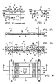
- FIGURES 3a and 3b are highly magnified schematic sectional views of successive steps in a fabrication process for producing a single ROM cell 70 according to the invention.
- the cell 70 is preferably formed at a face 72 of a p-type semiconductor layer 74.
- the lateral limits of the cell 70 are indicated by dashed lines 75.
- a nitride layer 76 is first formed across the semiconductor face 72.
- the nitride layer 76 is then patterned and etched to leave the portions shown in FIGURE 3a.
- a thick insulator layer 77 which for example may be oxide, is grown from those areas of the face 72 left exposed from the patterned and etched nitride layer 76.
- the nitride layer 76 is stripped and a gate oxide or other insulator layer 78 is grown over the structure. Most of this growth will occur on the areas of face 72 exposed by the removal of the nitride layer 76, as shown; there may be slight additions (not shown) to the thickness of thick oxide layer 77.
- a layer of conductive material such as highly doped amorphous or polycrystalline silicon or a metal, is deposited across the face of the structure. This conductive layer is patterned and etched to leave word line conductors 42a and 42b. Word line conductors 42a and 42b correspond to the word line conductor 42 of FIGURE 2. The word line conductor 42a defines a preselected programmed channel region 82.
- bit line region 54 is self-aligned to the edge of conductor 42a on one side and to the edges of thick insulator layer 77 on the remaining sides.
- Voltage source region 84 is partially self-aligned to an opposite edge of the thick insulator layer 77.
- One edge of the voltage source region 56 is self-aligned to the other edge of the word line conductor 42a.
- region 56 is preferably continuous with an (N+) implantation region that extends longitudinally parallel to conductor 42a. This implantation region is connected to ground or V ss .
- the voltage source region 84 is continuous with an elongate, longitudinally- oriented implantation region 88 that is connected to the voltage source V dd .
- region 86 is continuous with other voltage source regions 56 of other memory cells 70 in the row, while elongate region 88 is continuous with other voltage source regions 84 in the same row of memory cells 70.
- the lateral limits of one cell 70 are shown by a dashed rectangle 75. In a column direction, the cell 70 extends about half-way through the V ss region 86 on the one hand and about half-way through the V dd region 88 on the other.
- a further thick insulator layer 90 (omitted from FIGURE 4 for clarity) is deposited over the surface of the structure.
- a contact hole indicated generally at 92 is then opened in the thick insulator layer 90 and the gate insulator layer 78 to expose a portion of N+ region 54.
- the etching of opening 92 is followed by the deposition of a bit line conductor layer 44 such that hole 92 will be filled and the N+ bit line region will be contacted thereby.
- the lateral limits of the bit line conductor 44 are shown in FIGURE 4 by dashed lines 44. In a preferred embodiment, these are parallel to the limits 75 of cell 70 in a column direction.
- FIGURES 3b and 4 illustrate a read-only memory cell 70 that has been preselected or "programmed” to represent a logic zero, as a transistor has been formed between bit line region 54 and V ss region 56 while no transistor has been formed between region 54 and V dd region 84.
- the positioning (as shown in FIGURE 3b), of a portion of the thick insulator layer 77 is shifted from beneath the word line conductor 42b to beneath the word line conductor 42a.
- a transistor will be formed between the bit line region 54 and the V dd region 84, while no transistor region will be formed between the bit line region 54 and the V ss region 56.
- the positioning of the word line conductors 42a and 42b are not altered at all, and may be linear and parallel to each other up and down a row of memory cells 70.
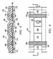
- FIGURES 5 and 6 are highly magnified sectional and plan views, respectively, of an alternative physical embodiment of a ROM cell according to the invention that is contact-programmable.
- a nitride layer (not shown) is grown on a surface 100 of a (p-) type semiconductor layer 102. This nitride layer is then patterned and etched to expose portions of the surface 100.
- a thick field oxide layer 104 is grown wherever the patterned and etched nitride layer (not shown) leaves the face 100 exposed. The nitride layer is then etched away.
- a gate oxide layer 106 is grown across the surface of the structure, with most of the growth occurring on the exposed regions of silicon not covered by the thick insulator layer 104.
- a highly doped layer of polycrystalline or amorphous silicon is deposited across the face of the structure and patterned and etched to leave a pair of polysilicon gates 108 and 110.
- the thick oxide layer 104 and the polysilicon gates 108 and 110 are next used as masking structures for an implantation step that forms (n+) regions 112, 114, 116 and 118.
- Diffused region 112 is connected to a V ss voltage source, and corresponds to region 86 shown in FIGURES 3b and 4.
- Region 118 is connected to V dd , and corresponds to the V dd region 88 of FIGURES 3b and 4.
- a first channel region 120 is defined underneath the gate 108 and between regions 112 and 114.
- a potential transistor indicated generally at 122 includes the drain region 114, the channel region 120, the source region 112 and the polysilicon gate 108.
- a second channel region 124 is defined underneath the polysilicon gate 110 and between the drain region 118 and the source region 116.
- a potential transistor indicated generally at 126 includes the drain region 118, channel region 124, source region 116 and the polysilicon gate 110.
- a contact indicated generally at 130 is next opened through the insulator layer 128 to a preselected, programmed one of the regions 114 and 116.
- a metal bit line 132 is thereafter deposited, patterned and etched to substantially fill the contact 130 and to extend in a column direction across the structure.
- FIGURE 6 is a schematic plan view corresponding to the sectional view of FIGURE 5.
- the thick insulator layer 128 and the gate oxide layer 106 have been omitted for the sake of clarity.
- the metal bit line 132 is represented by a pair of dashed horizontal lines. The boundary of this contact-programmable ROM cell is shown by the dashed enclosure 134.
- the cell of this embodiment is programmed by choosing to which of two regions 114 and 116 a word line contact is made. If a contact 130 is made to the region 116 as shown, a transistor will be connected between V dd region 118 and the word line 132. If, on the other hand, a contact is made to the region 114, a transistor will be connected between the V ss region 112 and the bit line 132.
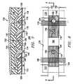
- FIGURE 7 is a highly magnified schematic sectional view of a via-programmable ROM cell. Since the contact-programmable cell shown in FIGURES 5 and 6 is similar in many respects to the via-programmable cell shown in FIGURES 7 and 8, like numbers identify like parts whereever possible throughout FIGURES 5-8.
- the fabrication of the via-programmable cell is similar to that of the contact-programmable cell.
- the initial fabrication steps are virtually identical.
- the first difference in the fabrication process occurs when two contacts 140 and 142 are opened through the thick insulator layer 128 to the respective diffused regions 114 and 116.
- a first metal layer is deposited, patterned and etched to form first metal straps 144 and 146.
- a second thick insulator layer 148 is deposited over the first thick insulator layer 128 and the straps 144 and 146.
- a via indicated generally at 150 is opened to a preselected, programmed one of the straps 144 and 146 to program the cell.
- a second metal bit line conductor 152 is then deposited, patterned and etched to fill the via 150 and make contact to the strap 146 as well as to extend across the cell in a column direction.
- FIGURE 8 A schematic plan view of the via-programmable cell is shown in FIGURE 8, with the insulator layers 106, 128 and 148 being omitted for clarity.
- the lateral limits of the cell are indicated by the dashed enclosure 134.
- the first metal straps 144 and 146 are indicated by horizontal shading.
- the metal 2 bit line 152 is represented by a pair of parallel dashed lines running in the row direction and covering the diffused regions 114 and 116.
- two potential transistors are once again formed, the first including regions 112, 114 and 120 and gate 108, and the second including regions 116, 118, 124 and gate 110.
- This cell is programmed by making a connection to one of the regions 114 and 116 through a respective one of the intervening metal straps 144 and 146.
- a transistor will either be connected between V dd and the metal 2 word line 152 or another transistor will be connected between V ss and the word line 152.
- a low-power dissipation static ROM cell and array has been shown and described that alternatively has formed therein a transistor between a bit line and V ss or between the bit line and V dd .
Landscapes
- Semiconductor Memories (AREA)
- Read Only Memory (AREA)
Applications Claiming Priority (2)
| Application Number | Priority Date | Filing Date | Title |
|---|---|---|---|
| US29049388A | 1988-12-27 | 1988-12-27 | |
| US290493 | 1988-12-27 |
Publications (2)
| Publication Number | Publication Date |
|---|---|
| EP0376568A2 true EP0376568A2 (fr) | 1990-07-04 |
| EP0376568A3 EP0376568A3 (fr) | 1991-01-09 |
Family
ID=23116255
Family Applications (1)
| Application Number | Title | Priority Date | Filing Date |
|---|---|---|---|
| EP19890313208 Withdrawn EP0376568A3 (fr) | 1988-12-27 | 1989-12-18 | Cellule semi-conductrice de mémoire morte et procédé de fabrication |
Country Status (3)
| Country | Link |
|---|---|
| EP (1) | EP0376568A3 (fr) |
| JP (1) | JPH02290067A (fr) |
| KR (1) | KR900010784A (fr) |
Cited By (3)
| Publication number | Priority date | Publication date | Assignee | Title |
|---|---|---|---|---|
| WO1996010266A1 (fr) * | 1994-09-28 | 1996-04-04 | Siemens Aktiengesellschaft | Dispositif de cellules de memoire a valeur fixe et son procede de fabrication |
| WO2001091185A3 (fr) * | 2000-05-19 | 2002-03-28 | Motorola Inc | Memoire rom a programmation ultra tardive et procede de fabrication |
| TWI668843B (zh) * | 2017-03-16 | 2019-08-11 | 日商東芝記憶體股份有限公司 | 半導體記憶體 |
-
1989
- 1989-12-18 EP EP19890313208 patent/EP0376568A3/fr not_active Withdrawn
- 1989-12-26 KR KR1019890019478A patent/KR900010784A/ko not_active Withdrawn
- 1989-12-27 JP JP1345027A patent/JPH02290067A/ja active Pending
Cited By (5)
| Publication number | Priority date | Publication date | Assignee | Title |
|---|---|---|---|---|
| WO1996010266A1 (fr) * | 1994-09-28 | 1996-04-04 | Siemens Aktiengesellschaft | Dispositif de cellules de memoire a valeur fixe et son procede de fabrication |
| US5973373A (en) * | 1994-09-28 | 1999-10-26 | Siemens Aktiengesellschaft | Read-only-memory cell arrangement using vertical MOS transistors and gate dielectrics of different thicknesses and method for its production |
| WO2001091185A3 (fr) * | 2000-05-19 | 2002-03-28 | Motorola Inc | Memoire rom a programmation ultra tardive et procede de fabrication |
| US6498066B2 (en) | 2000-05-19 | 2002-12-24 | Motorola, Inc. | Ultra-late programming ROM and method of manufacture |
| TWI668843B (zh) * | 2017-03-16 | 2019-08-11 | 日商東芝記憶體股份有限公司 | 半導體記憶體 |
Also Published As
| Publication number | Publication date |
|---|---|
| KR900010784A (ko) | 1990-07-09 |
| EP0376568A3 (fr) | 1991-01-09 |
| JPH02290067A (ja) | 1990-11-29 |
Similar Documents
| Publication | Publication Date | Title |
|---|---|---|
| US4373248A (en) | Method of making high density semiconductor device such as floating gate electrically programmable ROM or the like | |
| US4931847A (en) | Floating gate memory with sidewall tunnelling area | |
| US4603341A (en) | Stacked double dense read only memory | |
| US5168334A (en) | Non-volatile semiconductor memory | |
| EP0486249B1 (fr) | Réseau EPROM | |
| US5266507A (en) | Method of fabricating an offset dual gate thin film field effect transistor | |
| EP0020477B1 (fr) | Memoire a acces selectif dynamique | |
| US4493057A (en) | Method of making high density semiconductor device such as floating gate electrically programmable ROM or the like | |
| EP0552531A1 (fr) | Cellule de mémoire non-volatile et architecture en matrice | |
| EP0210809A1 (fr) | Mémoire non-volatile modifiable électriquement et son procédé de fabrication | |
| JPH07120719B2 (ja) | 半導体記憶装置 | |
| US6046482A (en) | Cell structure for mask ROM | |
| US5707884A (en) | Process for fabricating a contactless electrical erasable EPROM memory device | |
| US4380866A (en) | Method of programming ROM by offset masking of selected gates | |
| EP0043244B1 (fr) | Cellule à mémoire statique du type FET flip-flop à couche unique de silicium polycristallin | |
| US5227326A (en) | Method for fabricating non-volatile memory cells, arrays of non-volatile memory cells | |
| US6417548B1 (en) | Variable work function transistor high density mask ROM | |
| KR960012055B1 (ko) | 반도체집적회로장치 및 그 제조방법 | |
| EP0376568A2 (fr) | Cellule semi-conductrice de mémoire morte et procédé de fabrication | |
| US5245212A (en) | Self-aligned field-plate isolation between active elements | |
| US5942786A (en) | Variable work function transistor high density mask ROM | |
| US5329148A (en) | Semiconductor device and preparing method therefor | |
| US5828113A (en) | Double density MROM array structure | |
| US5027175A (en) | Integrated circuit semiconductor device having improved wiring structure | |
| US5329483A (en) | MOS semiconductor memory device |
Legal Events
| Date | Code | Title | Description |
|---|---|---|---|
| PUAI | Public reference made under article 153(3) epc to a published international application that has entered the european phase |
Free format text: ORIGINAL CODE: 0009012 |
|
| AK | Designated contracting states |
Kind code of ref document: A2 Designated state(s): DE FR GB IT NL SE |
|
| PUAL | Search report despatched |
Free format text: ORIGINAL CODE: 0009013 |
|
| AK | Designated contracting states |
Kind code of ref document: A3 Designated state(s): DE FR GB IT NL SE |
|
| 17P | Request for examination filed |
Effective date: 19910618 |
|
| 17Q | First examination report despatched |
Effective date: 19930211 |
|
| STAA | Information on the status of an ep patent application or granted ep patent |
Free format text: STATUS: THE APPLICATION IS DEEMED TO BE WITHDRAWN |
|
| 18D | Application deemed to be withdrawn |
Effective date: 19930824 |