EP0376721A2 - Feuchtigkeitsdetektor - Google Patents
Feuchtigkeitsdetektor Download PDFInfo
- Publication number
- EP0376721A2 EP0376721A2 EP89313646A EP89313646A EP0376721A2 EP 0376721 A2 EP0376721 A2 EP 0376721A2 EP 89313646 A EP89313646 A EP 89313646A EP 89313646 A EP89313646 A EP 89313646A EP 0376721 A2 EP0376721 A2 EP 0376721A2
- Authority
- EP
- European Patent Office
- Prior art keywords
- moisture
- substrate
- sensitive device
- heating elements
- film
- Prior art date
- Legal status (The legal status is an assumption and is not a legal conclusion. Google has not performed a legal analysis and makes no representation as to the accuracy of the status listed.)
- Granted
Links
Images





Classifications
-
- G—PHYSICS
- G01—MEASURING; TESTING
- G01N—INVESTIGATING OR ANALYSING MATERIALS BY DETERMINING THEIR CHEMICAL OR PHYSICAL PROPERTIES
- G01N27/00—Investigating or analysing materials by the use of electric, electrochemical, or magnetic means
- G01N27/02—Investigating or analysing materials by the use of electric, electrochemical, or magnetic means by investigating impedance
- G01N27/04—Investigating or analysing materials by the use of electric, electrochemical, or magnetic means by investigating impedance by investigating resistance
- G01N27/14—Investigating or analysing materials by the use of electric, electrochemical, or magnetic means by investigating impedance by investigating resistance of an electrically-heated body in dependence upon change of temperature
- G01N27/18—Investigating or analysing materials by the use of electric, electrochemical, or magnetic means by investigating impedance by investigating resistance of an electrically-heated body in dependence upon change of temperature caused by changes in the thermal conductivity of a surrounding material to be tested
Definitions
- a typical absolute humidity sensor is shown in Fig. 9, where insulating layers 2 are formed on the surface of a substrate 1.
- a bridge 3c made of an insulating thin film is formed over one insulating layer 2.
- a heating element 15 made of a thin film of a thermistor material is formed on the bridge 3c. The heat capacity of this device is very small.
- the insulating thin film can assume the form of a cantilever or a diaphragm, as well as the form of a bridge.
- the thermistor material can be SiC, TaN, Ge, or other material.
- An absolute humidity sensor using a thin-film heating element made from such a thermistor material shows high response speed and high sensitivity, but the thin film is not stable over a long term. Especially, it is not stable against heat. Further, the device is not easy to manufacture, because it is necessary to form electrodes 16, and for other reasons.
- a detector element and a reference element are formed on a single substrate to provide temperature compensation.
- the reference element is hermetically sealed.
- this humidity sensor also suffers from the above-described drawbacks, since it uses a thermistor material.
- a flow sensor using a heating element made of a thin film of platinum is known.
- the heating element of this sensor is shaped like a bridge in the same way as the device described in connection with Fig. 9.
- This flow sensor can operate from room temperature to 50°C or below.
- the heating element is exposed to the surrounding environment so that it may be directly subjected to flow of the environment.
- a moisture-sensitive device comprising: a substrate provided with a pair of recesses; a pair of belt-like heating elements extending over the recesses and formed on the same side as, or opposite side of, the openings of the recesses; an insulator formed between the substrate and the heating elements; a container the inside of which is an atmosphere of a given humidity, the container being formed integral with the substrate and acting to isolate one of the heating elements from the outside atmosphere; lead wires for supplying electric current to the heating elements; and the heating element being a resistive film of platinum or nickel and a heat resistant insulating film covering the resistive film.
- a moisture-sensitive device includes a substrate which is provided with at least one pair of recesses. These recesses are so shaped as to be contributable to a reduction in the heat capacity of the finished moisture-sensitive device and also to sufficient heat insulation from belt-like heating elements (described later). Preferably, the recesses are shaped into substantially the same form. The low heat capacity and the heat insulation from the belt-like heating elements described above are of importance for the reasons described below.
- the amount of dissipated heat q is represented in kcal/h.
- the dissipated heat amount q can be increased by increasing (T-T0), i.e., elevating the temperature T of the device.
- T-T0 i.e., elevating the temperature of the device.
- the measures taken are only to increase the operating temperature of the device, then the amount of electric power consumed by the device increases greatly. This leads to a great decrease in the speed of response of the device to heat, which will result in a substantial reduction in the speed of response to water vapor. Therefore, it is important to reduce the heat capacity of the device, i.e., to provide sufficient heat insulation from the heating elements of the device, for realizing high-speed response, low power consumption, and high-temperature operation.
- the novel moisture-sensitive device is equipped with a pair of belt-like heating elements, corresponding to the above-described recesses.
- the heating elements are supported on the substrate via an insulator and disposed close to the opening of the recesses, or the heating elements are disposed via an insulator on the surface of the substrate which is on the opposite side of the recesses.
- the elements can be supported by a bridge-shaped, cantilever-shaped, or otherwise shaped structure.
- the heating elements are supported by a diaphragm-shaped structure, for example.
- Each of the belt-like heating elements consists of a resistive film of platinum or nickel and a heat-resistant insulating film that covers the resistive film.
- the resistive film shows excellent stability at high temperatures. As the operating temperature of the belt-like heating elements of the moisture-sensitive device is increased, higher sensitivity is obtained, because the difference between the output signals produced from moist air and dry air increases.
- the resistive film of platinum or nickel operates reliably within a high-temperature range of 300 to 400°C.
- the prior art device using thermistors can operate only up to about 200°C. In this way the novel device exhibits unparalleled response characteristics. Platinum is preferable to nickel., since platinum is more resistant to oxidation at high temperature.
- One of the belt-like heating elements is formed into a reference element, while the other is formed into a detector element.
- the heating element forming the reference element is hermetically sealed by a sealing cap coupled to the substrate, and isolated from the outside atmosphere.
- the inside of the cap constitutes a given moist atmosphere which can include dry condition.
- the belt-like heating element forming the detector element may be designed to be exposed to the outside atmosphere. This detector element may also be formed simply by exposing the belt-like heating element to the outside atmosphere.
- a sealing cap is used for the reference element, and the cap is provided with holes that open into the outside atmosphere. In this case, the holes may be formed at any arbitrary positions. Where a multiplicity of moisture-sensitive devices are formed on a single wafer, water is used to cut the wafer into individual devices, or dice. In order to prevent the water from entering the cap, it is desired to form the holes at the junction of the substrate and the cap.
- the belt-like heating elements can be formed and held on the substrate by micromachining techniques used in semiconductor fabrication processes such as thermal oxidation, sputtering, vapor deposition in vacuum, other film-forming techniques, and photolithography.
- Micromachining techniques such as etching or photolithography can be directly applied to the fabrication of the sealing cap.
- the cap can be joined by screen printing, coating, sintering, or other process. These techniques are described in detail in the description of examples of the invention.
- the belt-like reference element and the belt-like detector element are held on the same substrate by similar structures. It is desired that the two belt-like heating elements be hermetically sealed in an enclosure and that the heating elements be sealed by their respective casings within the enclosure.
- the casing sealing the detector element is provided with thin holes for communication with the outside atmosphere.
- the novel moisture-sensitive device is designed so that the amount of water vapor contained in the detected atmosphere is measured from the difference between the outputs form the reference element and the detector element, utilizing the difference in resistance between both elements.
- a bridge circuit is built from the lead wires bonded to both heating elements. When the bridge circuit is not balance, the produced output is used as the detector output. This is described in greater detail in the description of examples of the invention.
- the heating elements are heated by their respective resistive films made from platinum or nickel that is stable against heat.
- the amount o of heat dissipated away to the substrate is suppressed, because the recesses are formed in the substrate, and because the belt-like heating elements are supported by a bridge-, cantilever- or diaphragm-shaped structure. Therefore, the amount of heat dissipated depends upon the heat conduction coefficient of the atmosphere that is determined by the amount of water vapor contained in the atmosphere surrounding the heating element. Consequently, the change in the amount of heat dissipated by the heating elements reflects the change in the humidity of the surrounding atmosphere. The changes in the resistance values of the resistive films.
- One of the heating elements is hermetically sealed within an atmosphere of a given humidity, while the other is exposed to the detected atmosphere. Hence, the difference between the outputs from the heating elements is not affected by the temperature of the atmosphere.
- the novel moisture-sensitive device has the following practical advantages.
- Fig. 1 shows a recess formed in a moisture-sensitive device according to the invention and a belt-like heating element disposed at the position of the opening of the recess.
- Fig. 1(A) is a schematic plan view of these portions of the device.
- Fig. 1(B) is a cross-sectional view taken along line X-X of Fig. 1(A).
- Fig. 1(C) is a cross-sectional view taken along line Y-Y of Fig. 1(A).
- An insulating layer 2 made of a thin film is formed on a substrate 1 of silicon. The layer 2 is shaped like a bridge.
- the substrate 1 of silicon is etched anisotropically along the crystallographic axis to form a hollow structure between the substrate 1 and a micro bridge 3 formed from the insulating layer.
- the device is excellent in thermal insulation and has a small heat capacity.
- a resistive thin film 4 made from a sensor material is formed into a desired pattern on the micro bridge 3 so as to obtain a desired resistance value.
- a protective film 5 made from an insulating material is formed on the resistive film 4.
- the thin insulating layer 2 of SiO2, Si3N4, Al2O3, or other material is formed on the substrate 1 of silicon by thermal oxidation, sputtering, vapor evaporation in vacuum, or chemical vapor deposition, depending on the material.
- the chemical etching rate differs with the orientation of crystallographic axis.
- the insulating layer 2 underlies the micro bridge 3.
- a film of SiO2 is formed by thermal oxidation to prevent formation of etch pits when the silicon substrate is etched later.
- a metal such as platinum or nickel which has a large temperature coefficients of resistance are sputtered of deposited on the insulating layer 2 in a vacuum.
- the metal layer is formed into a desired pattern on the portion which forms the micro bridge 3 on the insulating layer when the silicon substrate is etched later.
- the patterning is conducted by photolithography and dry etching or chemical etching.
- the patterned metal layer forms the resistive film 4 having a desired resistance value.
- the resistive film 4 is made from platinum which is stable against chemicals and also against heat.
- the film 4 is formed into a zigzag or meandering pattern by dry etching as shown in Fig. 2. At this time, the platinum film has a thickness of 2000 to 5000 ⁇ , typically 5000 ⁇ .
- the meandering pattern has a width of 1 to 10 ⁇ m, typically 5 ⁇ m.
- the upper insulating layer 5 which serves as a protective film is formed on the resistive film 4 by sputtering, vapor deposition in vacuum, thermal oxidation, chemical vapor deposition, or other process.
- the insulating layer 5 acts as a mask when the silicon substrate is etched later.
- a film of Al2O3 which adheres well to platinum and exhibits good weatherproofness is formed by sputtering.
- the portion of the silicon substrate which is located under the lower insulating layer 2 is selectively etched away to form the micro bridge 3 consisting of the upper insulating layer 5, the lower insulating layer 2, and the resistive film 4.
- the upper and lower insulating layers are etched into a bridge pattern by photolithography, chemical etching, and dry etching to expose the silicon substrate located under the insulating layers.
- the upper insulating layer is etched into a bonding pad with which lead wires extending to the platinum film are connected. More specifically, the film of Al2O3 is chemically etched, using a solution of phosphoric acid.
- the layer of SiO2 is treated by chemical etching or dry etching, depending on the thickness of the film.
- the platinum resistive film is exposed.
- the exposed film of platinum is resistant to the etchant and stable, whether the etching is chemical etching or dry etching. Therefore, the pad 6 can be created will.
- the exposed portions of the silicon substrate are chemically etched, using an alkaline solution of ethylenediamine pyrocatechol or KOH, so that the silicon crystal is anisotropically etched.
- the silicon substrate located under the insulating layer is etched into a bridge pattern to form the micro bridge 3 consisting of the upper insulating layer 5, the lower insulating layer 2, and the resistive film 4.
- the upper and lower insulating layers can be films of Si3N4, which are similar in characteristic to the film of Al2O3
- the upper and lower insulating layers are used as masks for the anisotropic etching. When the (111) plane of the (100) silicon substrate is exposed, the etching is performed.
- FIG. 3(A) is a perspective view of the element.
- Fig. 3(B) is a cross-sectional view taken on line X-X of Fig. 3(A).
- Fig. 3(C) is a cross-sectional view taken on line Y-Y of Fig. 3(A).
- This element has a resistive layer 4 on an insulating, cantilever-shaped layer 7 which is formed by patterning an upper insulating layer 5 and a lower insulating layer 2.
- This element is slightly inferior in mechanical strength to the above-described element but provides better thermal insulation.
- the fundamental micro bridge type device and cantilever type device are formed by the processes described above.
- the meandering patter of the platinum resistive film is electrically energized and heats up to a certain temperature, the temperature changes according to changes in the amount of water vapor. This temperature change varies the resistance value. In this way, the amount of water vapor can be detected.
- FIG. 4(A) is a perspective view of the element.
- Fig. 4(B) is a cross-sectional view taken on line X-X of Fig. 4(A).
- Fig. 4(C) is a cross-sectional view taken on line Y-Y of Fig. 4(A).
- An insulating thin film 2a is formed on the front surface, the rear surface, and the side surfaces of a silicon substrate 1a.
- the insulating layer 2a on the rear surface of the silicon substrate 1a is etched into a desired form having desired dimensions according to the pattern needed to create a diaphragm. Thus, a mask for anisotropic etching is created.
- the anisotropic etching is started from the center of the rear surface of the silicon substrate 1a on which the insulating layer 2a is not formed. The central portion of the silicon substrate 1a is then thinned. A diaphragm 13 consisting of the tin insulating layer formed on the silicon substrate 1a and a layer of the silicon substrate material is formed. A resistive thin film 4a of nickel is formed on the diaphragm 13. The film 4a is formed into a desired form having specified dimensions, such as meandering pattern similar to the pattern shown in Fig. 2. A protective film is formed on the resistive film. In this way, an element including the diaphragm 13 is fabricated.
- the diaphragm comprises the silicon layer doped with boron and the insulating layer. It is not always necessary to control the thickness of the silicon layer by doping it with boron. It is also possible to control it by controlling only the time of for which anisotropic etching is carried out. Further, this portion of the silicon layer may be fully etched away to form the diaphragm only form the insulating layer.
- the thermal insulation of the resistive film of the diaphragm type moisture-sensitive element manufactured in this way is much superior to the thermal insulation of the resistive film of the prior art thermal conduction type moisture-sensitive element. That is, the novel element has a much reduced heat capacity.
- the diaphragm type element is somewhat inferior in response characteristic to the bridge type and cantilever type elements.
- the diaphragm type element is superior to the bridge type and cantilever type elements, because the mechanical strength of the diaphragm is excellent. Accordingly, the diaphragm type element which has high sensitivity, high-speed response, and low consumption of electrical power can be advantageously used in environment requiring high mechanical strength.
- a moisture-sensitive device equipped with a pair of elements of the structure described above are next described.
- the elements are formed on a single substrate.
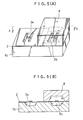
- Fig. 5 shows the structure of a moisture-sensitive device according to the invention.
- Fig. 5(A) is a perspective view of the device.
- Fig. 5(B) is a cross-sectional view taken on line X-X′ of Fig. 5(A).
- This devices includes a substrate 1b on which a pair of micro bridge elements having the same characteristics is formed. Each micro bridge element is the same as the micro bridge element shown in Fig. 1 and has a resistive film of platinum.
- One of the elements is a detector element 3a, while the other is a reference element 3b.
- a sealing cap (hereinafter referred to as the micro cap) is placed over the reference element 3b to isolate it from the outside atmosphere.
- the cap is bonded to the substrate with a low-melting glass or adhesive.
- the cap that takes the form of a container is created by half etching a box-like silicon block form its one side.
- the reference element 3b is hermetically sealed within the micro cap and so the reference
- Fig. 6 shows the structure of another moisture-sensitive device according to the invention.
- Fig. 6(A) is a perspective view of the device.
- Fig. 6(B) is a cross-sectional view taken on line X-X′ of Fig. 6(A).
- This device includes a substrate 1c on which a pair of micro bridge elements having the same characteristics is formed.
- Each micro bridge element has a resistive film of platinum and is the same as the micro bridge element shown in Fig. 1.
- One of the micro bridge elements is a detector element 3a, whereas the other is a reference element 3b.
- the elements 3a and 3b are hermetically sealed in a sealing micro cap 8a taking the form of a container.
- the cap 8a is fabricated by anisotropically etching silicon.
- the detector element 3a is provided with minute holes 11 to permit water vapor to go into and out of the element.
- the reference element 3b is hermetically sealed as mentioned above to prevent water vapor from going into and out
- a bridge circuit built as shown in Fig. 7 includes the resistive films of platinum of the elements 3a and 3b obtained in this way.
- the bridge circuit delivers an output signal V OUT .
- the noise introduced in the output due to variations in the temperature of the atmosphere can be canceled out.
- the output signal reflecting only the variations in the amount of water vapor is derived accurately. That is, the dependence of the response to humidity upon temperature can be compensated for, using the reference element 3b.
- a film of SiO2 is formed over the whole surface of a substrate of silicon by thermal oxidation. Then, the film of SiO2 is etched into a desired pattern on both sides of the substrate by photolithography and chemical etching or dry etching. At this time, two recesses 9 and 10 in the micro cap and the minute holes 11 permitting water vapor to go into and out of the element 3a. Then, the exposed portions of silicon are anisotropically etched, using an alkaline solution of ethylenediamine pyrocatechol or KOH, in the same way as the elements of the body. Thus, the micro cap 8 is obtained. Finally, the micro cap is joined to the elements of the body to manufacture the moisture- sensitive device shown in Fig. 6.
- variable resistor as R4 21.
- the resistive film 18 of platinum of the detector element is affected by the variation and the temperature of the element changes.
- the resistance value of the detector element varies, unbalancing the bridge circuit.
- a voltage corresponding to the amount of water vapor is obtained at the output V OUT 22.
- the temperature of the atmosphere changes, the temperature of the two elements change by the same amount, and their resistance values change by the same amount.
- the output a V OUT 22 is maintained at the reference level and does not vary. In this way, the dependence of the response to the humidity upon temperature is considerably compensated for. This enables accurate detection.
- the output signal from the novel device is superior in signal-to-noise ratio to the output from the prior art sealed package type device.
- Fig. 8 show a still other moisture-sensitive device according to the invention.
- Fig. 8(A) is a plan view of the device.
- Fig. 8(B) is a cross-sectional view taken along line X-X of Fig. 8(A).
- This moisture-sensitive device includes a substrate 1d and a pair of micro bridge elements of the construction shown in Fig. 1. The elements are formed on the substrate 1d and have the same characteristics. Each micro bridge element has a resistive film of platinum. One of the elements is a detector element 3a, while the other is a reference element 3b.
- a micro cap 8b is provided with recesses corresponding to the position of the substrate 1d.
- the cap 8b is formed with cutouts for exposing the bonding pads 6b of the elements 3a and 3b.
- the recesses form spaces for the elements.
- Low-melting glass paste 12a for joining the cap to the substrate is applied to the micro cap 8b by screen printing in a pattern indicated by the hatching in Fig. 8(A).
- the paste is provisionally sintered to evaporate the solvent contained in the paste.
- the substrate 1d and the micro cap 8b are placed in an opposite relation to each other within an atmosphere of dry air or air of a known humidity sealed in the space of the reference element 3b.
- the substrate 1d and the micro cap 8b are so arranged that their recesses together from spaces surrounding the elements 3a and 3b, respectively.
- a plurality of moisture-sensitive device of the construction described above are batched on a silicon substrate and then they are separated by dicing.
- Each chip, or moisture-sensitive device, separated as described above is mounted on an electronic part stem. Wires are bonded to the pads 6b. Then, a mesh cap is placed on the chip to complete the moisture-sensitive device.
- the sensitivities of the devices (a) and (a′) according to the invention are twice as high as the sensitivity of the conventional device (b) and eight times as high as the sensitivity of the conventional device (c).
- the devices (a) and (a′) were operated at temperatures of about 300°C.
- the device (b) was operated at about 150°C.
- the device (c) was operated at approximately 200°C. At these temperatures, the device operated reliably as described later.
- the speeds of response to moisture of the devices (a) and (c) are compared in Fig. 12.
- the used circuit and the operating temperatures were the same as those used in the above-described experiments on sensitivities (Fig. 11).
- the response characteristics of the circuit obtained when the humidity of the atmosphere was changed rapidly from 10 g/m3 to 35 g/m3 at temperature 40°C are shown.
- the response time of the novel device (a) was about 5 sec, while the response time of the conventional device (c) was about 50 sec.
- the device (a) according to the invention is about ten times as high as the response time of the conventional device (c).
- the device (c) consumed electric power of about hundreds of milliwatts, whereas the device (a) consumed electric power of tens of milliwatts. In this way, the invention achieves a great reduction in the consumed electric power.
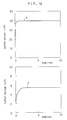
- the stability at high temperatures of the platinum resistive film was compared with the stability at high temperatures of the thin thermistor film, for checking their reliability.
- the devices (a) and (b) were electrically energized at room temperature, so that they were heated to about 400°C and 200°C, respectively. Then, they were allowed to stand.
- the ratio of the resistance value R0 at evaluating temperature of 0°C to its initial value was measured.
- the ratios of the devices changed with time as shown in Fig. 13.
- the ratio increased at high rates.
- the novel device (a) having the platinum resistive film the ratio was quite stable. Hence, the device (a) is highly reliable.
- the inventive moisture-sensitive device having platinum resistive films on a micro bridge-, cantilever-, or diaphragm-shaped insulating layer operates stably over a long term, consumes much less electric power than the prior art device, responds at a high speed, and exhibits high sensitivity.
Landscapes
- Chemical & Material Sciences (AREA)
- Chemical Kinetics & Catalysis (AREA)
- Electrochemistry (AREA)
- Physics & Mathematics (AREA)
- Health & Medical Sciences (AREA)
- Life Sciences & Earth Sciences (AREA)
- Analytical Chemistry (AREA)
- Biochemistry (AREA)
- General Health & Medical Sciences (AREA)
- General Physics & Mathematics (AREA)
- Immunology (AREA)
- Pathology (AREA)
- Investigating Or Analyzing Materials By The Use Of Fluid Adsorption Or Reactions (AREA)
- Investigating Or Analyzing Materials By The Use Of Electric Means (AREA)
- Investigating Or Analyzing Materials Using Thermal Means (AREA)
Applications Claiming Priority (4)
| Application Number | Priority Date | Filing Date | Title |
|---|---|---|---|
| JP332348/88 | 1988-12-29 | ||
| JP63332348A JPH0795054B2 (ja) | 1988-12-29 | 1988-12-29 | 湿度センサ |
| JP1229873A JPH06100568B2 (ja) | 1989-09-05 | 1989-09-05 | 雰囲気センサ |
| JP229873/89 | 1989-09-05 |
Publications (3)
| Publication Number | Publication Date |
|---|---|
| EP0376721A2 true EP0376721A2 (fr) | 1990-07-04 |
| EP0376721A3 EP0376721A3 (fr) | 1991-01-30 |
| EP0376721B1 EP0376721B1 (fr) | 1998-07-15 |
Family
ID=26529040
Family Applications (1)
| Application Number | Title | Priority Date | Filing Date |
|---|---|---|---|
| EP89313646A Expired - Lifetime EP0376721B1 (fr) | 1988-12-29 | 1989-12-28 | Feuchtigkeitsdetektor |
Country Status (3)
| Country | Link |
|---|---|
| US (1) | US5048336A (fr) |
| EP (1) | EP0376721B1 (fr) |
| DE (1) | DE68928739T2 (fr) |
Cited By (8)
| Publication number | Priority date | Publication date | Assignee | Title |
|---|---|---|---|---|
| WO1994010822A1 (fr) * | 1992-10-26 | 1994-05-11 | THE UNITED STATES OF AMERICA as represented by THEUNITED STATES DEPARTMENT OF COMMERCE | Dispositifs a micro-plaque chauffante et procedes de fabrication |
| EP0640830A1 (fr) * | 1993-08-23 | 1995-03-01 | Vaisala Oy | Capteur et procédé de détection d'un liquide et/ou d'un changement de phase |
| EP0675354A4 (fr) * | 1993-10-19 | 1996-11-29 | Jury Gennadievich Usanov | Jauge hygrometrique. |
| WO2002006808A1 (fr) * | 2000-07-19 | 2002-01-24 | Lg Electronics Inc. | Capteur d'humidite absolue |
| EP1203956A3 (fr) * | 2000-11-01 | 2003-10-22 | Roche Diagnostics GmbH | Biocapteurs avec un canal d'écoulement |
| US6695469B2 (en) | 2001-11-19 | 2004-02-24 | Energy Absorption Systems, Inc. | Roadway freezing point monitoring system and method |
| CN101034076B (zh) * | 2006-03-10 | 2010-10-06 | 财团法人工业技术研究院 | 悬臂式电阻湿度感测结构及其制法 |
| EP2290357A1 (fr) * | 2009-08-28 | 2011-03-02 | Hitachi Automotive Systems, Ltd. | Capteur d'humidité thermique |
Families Citing this family (34)
| Publication number | Priority date | Publication date | Assignee | Title |
|---|---|---|---|---|
| WO1994028372A1 (fr) * | 1993-05-25 | 1994-12-08 | Rosemount Inc. | Capteur chimique organique |
| US5423212A (en) * | 1993-06-18 | 1995-06-13 | Ricoh Seiki Company, Ltd. | Flow sensor |
| US5388443A (en) * | 1993-06-24 | 1995-02-14 | Manaka; Junji | Atmosphere sensor and method for manufacturing the sensor |
| FI96640C (fi) * | 1993-08-23 | 1996-07-25 | Vaisala Oy | Menetelmä suhteellisen kosteuden mittaamiseksi, etenkin radiosondeissa |
| US5837884A (en) * | 1994-12-29 | 1998-11-17 | Tokin Corporation | Humidity sensor using temperature sensing resistor controlled to be at constant temperature of more than 150° C. |
| JP3494747B2 (ja) * | 1995-03-31 | 2004-02-09 | 石塚電子株式会社 | 薄膜温度センサ及びその製造方法 |
| US5563341A (en) * | 1995-06-07 | 1996-10-08 | Fenner; Ralph L. | Vapor pressure sensor and method |
| DE19524943C2 (de) * | 1995-07-08 | 2003-05-08 | Siemens Ag | Sensor |
| US5783743A (en) * | 1995-07-08 | 1998-07-21 | Vdo Adolf Schindling Ag | Moisture sensor |
| DE19610293C1 (de) * | 1996-03-15 | 1997-07-31 | Fraunhofer Ges Forschung | Vorrichtung zur gekapselten Aufnahme eines Materials |
| DE19644575C1 (de) * | 1996-10-26 | 1998-01-08 | Barbara Dr Pause | Verfahren und Vorrichtung zur Messung der Wasserdampfdiffusion durch plattenförmige, poröse Proben, insbesondere durch textile Flächengebilde, unter verschiedenen Meßbedingungen |
| US6038922A (en) * | 1997-06-19 | 2000-03-21 | Agilent Technologies, Inc. | Thermometric apparatus and method for determining the concentration of a vapor in a gas stream |
| US6202480B1 (en) | 1998-04-02 | 2001-03-20 | Agilent Technologies, Inc. | Thermometric vapor sensor with evaporation surface having micropores |
| KR100351810B1 (ko) * | 1999-12-13 | 2002-09-11 | 엘지전자 주식회사 | 절대습도센서 |
| USD475639S1 (en) | 2000-11-17 | 2003-06-10 | Cogiscan, Inc. | Clip for electronic component tray |
| JP3678180B2 (ja) * | 2001-07-27 | 2005-08-03 | 株式会社デンソー | フローセンサ |
| RU2224246C1 (ru) * | 2002-07-10 | 2004-02-20 | Воронежский государственный технический университет | Микроэлектронный датчик влажности поверхностно-конденсационного типа |
| WO2007054847A2 (fr) * | 2005-11-09 | 2007-05-18 | Koninklijke Philips Electronics N.V. | Procede pour produire un support de boitier destine a renfermer au moins un element microelectronique, et procede pour produire un dispositif de diagnostic |
| TWI279536B (en) * | 2006-02-24 | 2007-04-21 | Ind Tech Res Inst | Cantilever resistive humidity detection structure and method for manufacturing the same |
| US7898365B2 (en) * | 2006-09-06 | 2011-03-01 | Raytheon Company | Integrated saw device heater |
| TWI319479B (en) * | 2006-10-18 | 2010-01-11 | Ind Tech Res Inst | A resistive-type humidity sensing structure with micro-bridge format and a method therefor |
| RU2369863C2 (ru) * | 2007-12-12 | 2009-10-10 | Федеральное государственное унитарное предприятие "Государственный научный центр Российской Федерации-Физико-энергетический институт имени А.И. Лейпунского" | Устройство для измерения влажности воздуха |
| US8393785B2 (en) * | 2009-05-14 | 2013-03-12 | Palo Alto Research Center Incorporated | Nanocalorimeter based on thermal probes |
| US8130072B2 (en) * | 2009-05-14 | 2012-03-06 | Palo Alto Research Center Incorporated | Vanadium oxide thermal microprobes |
| US9232315B2 (en) | 2011-03-16 | 2016-01-05 | Phonon Corporation | Monolithically applied heating elements on saw substrate |
| US9103705B2 (en) | 2012-02-27 | 2015-08-11 | Freescale Semiconductor, Inc. | Combined environmental parameter sensor |
| US20150377813A1 (en) * | 2014-06-30 | 2015-12-31 | Stmicroelectronics S.R.L. | Semiconductor gas sensor device and manufacturing method thereof |
| DE102015209200B3 (de) * | 2015-05-20 | 2016-03-10 | Siemens Aktiengesellschaft | Wärmeleitfähigkeitsdetektor |
| WO2017091907A1 (fr) * | 2015-12-04 | 2017-06-08 | Instrumar Limited | Appareil et procédé de détection de brèches dans des conduites |
| JP6685789B2 (ja) * | 2016-03-24 | 2020-04-22 | ヤマハファインテック株式会社 | ガスセンサ |
| WO2020031517A1 (fr) * | 2018-08-10 | 2020-02-13 | Tdk株式会社 | Capteur de gaz |
| US11397047B2 (en) * | 2019-04-10 | 2022-07-26 | Minebea Mitsumi Inc. | Moisture detector, moisture detection method, electronic device, and log output system |
| DE102019130755A1 (de) * | 2019-11-14 | 2021-05-20 | Tdk Corporation | Sensorvorrichtung, Verfahren zum Herstellen einer Sensorvorrichtung und Sensorbaugruppe |
| DE102022107394A1 (de) * | 2021-03-30 | 2022-10-06 | Tdk Electronics Ag | Sensorsystem, Sensoranordnung und Verfahren zur Verwendung des Sensorsystems |
Family Cites Families (13)
| Publication number | Priority date | Publication date | Assignee | Title |
|---|---|---|---|---|
| US4419888A (en) * | 1979-06-14 | 1983-12-13 | Kabushikikaisha Shibaura Denshi Seisakusho | Humidity measuring method |
| US4562725A (en) * | 1982-07-31 | 1986-01-07 | Shimadzu Corporation | Moisture sensor and a process for the production thereof |
| CA1216330A (fr) * | 1983-02-07 | 1987-01-06 | Junji Manaka | Detecteur faible puissance pour gaz |
| JPS61201148A (ja) * | 1985-03-04 | 1986-09-05 | Richo Seiki Kk | 発熱体支持構造 |
| GB2172999A (en) * | 1985-03-25 | 1986-10-01 | Protimeter Plc | A humidity measurement or control instrument |
| JPH0517650Y2 (fr) * | 1986-01-31 | 1993-05-12 | ||
| JPH0795002B2 (ja) * | 1987-04-22 | 1995-10-11 | シャープ株式会社 | センサ素子 |
| US4928513A (en) * | 1986-07-29 | 1990-05-29 | Sharp Kabushiki Kaisha | Sensor |
| JPS63145954A (ja) * | 1986-07-29 | 1988-06-18 | Sharp Corp | 感湿素子 |
| EP0265834B1 (fr) * | 1986-10-28 | 1992-07-22 | Figaro Engineering Inc. | Capteur et méthode pour sa fabrication |
| JPS63201559A (ja) * | 1987-02-17 | 1988-08-19 | Sharp Corp | 検知素子 |
| JPH0814554B2 (ja) * | 1987-02-18 | 1996-02-14 | 三洋電機株式会社 | 湿度検出装置 |
| JPH0650255B2 (ja) * | 1987-03-31 | 1994-06-29 | シャープ株式会社 | シリコンマイクロセンサの製造方法 |
-
1989
- 1989-12-28 EP EP89313646A patent/EP0376721B1/fr not_active Expired - Lifetime
- 1989-12-28 DE DE68928739T patent/DE68928739T2/de not_active Expired - Fee Related
- 1989-12-29 US US07/459,262 patent/US5048336A/en not_active Expired - Lifetime
Cited By (14)
| Publication number | Priority date | Publication date | Assignee | Title |
|---|---|---|---|---|
| US5464966A (en) * | 1992-10-26 | 1995-11-07 | The United States Of America As Represented By The Secretary Of Commerce | Micro-hotplate devices and methods for their fabrication |
| WO1994010822A1 (fr) * | 1992-10-26 | 1994-05-11 | THE UNITED STATES OF AMERICA as represented by THEUNITED STATES DEPARTMENT OF COMMERCE | Dispositifs a micro-plaque chauffante et procedes de fabrication |
| EP0640830A1 (fr) * | 1993-08-23 | 1995-03-01 | Vaisala Oy | Capteur et procédé de détection d'un liquide et/ou d'un changement de phase |
| US5619144A (en) * | 1993-08-23 | 1997-04-08 | Vaisala Oy | Detector and method for observation of the presence of a liquid and/or of a change of phase in same |
| EP0675354A4 (fr) * | 1993-10-19 | 1996-11-29 | Jury Gennadievich Usanov | Jauge hygrometrique. |
| US6840103B2 (en) | 2000-07-19 | 2005-01-11 | Lg Electronics Inc. | Absolute humidity sensor |
| WO2002006808A1 (fr) * | 2000-07-19 | 2002-01-24 | Lg Electronics Inc. | Capteur d'humidite absolue |
| EP1203956A3 (fr) * | 2000-11-01 | 2003-10-22 | Roche Diagnostics GmbH | Biocapteurs avec un canal d'écoulement |
| US6911621B2 (en) | 2000-11-01 | 2005-06-28 | Roche Diagnostics Corporation | Biosensor |
| US6695469B2 (en) | 2001-11-19 | 2004-02-24 | Energy Absorption Systems, Inc. | Roadway freezing point monitoring system and method |
| US7090392B2 (en) | 2001-11-19 | 2006-08-15 | Energy Absorption Systems, Inc. | Roadway freezing point monitoring system and method |
| CN101034076B (zh) * | 2006-03-10 | 2010-10-06 | 财团法人工业技术研究院 | 悬臂式电阻湿度感测结构及其制法 |
| EP2290357A1 (fr) * | 2009-08-28 | 2011-03-02 | Hitachi Automotive Systems, Ltd. | Capteur d'humidité thermique |
| US8359919B2 (en) | 2009-08-28 | 2013-01-29 | Hitachi Automotive Systems, Ltd. | Thermal humidity sensor |
Also Published As
| Publication number | Publication date |
|---|---|
| US5048336A (en) | 1991-09-17 |
| EP0376721A3 (fr) | 1991-01-30 |
| DE68928739T2 (de) | 1999-02-11 |
| EP0376721B1 (fr) | 1998-07-15 |
| DE68928739D1 (de) | 1998-08-20 |
Similar Documents
| Publication | Publication Date | Title |
|---|---|---|
| EP0376721B1 (fr) | Feuchtigkeitsdetektor | |
| US4928513A (en) | Sensor | |
| KR100379471B1 (ko) | 절대습도센서 및 이를 이용한 온/습도 검출 회로 | |
| Dibbern | A substrate for thin-film gas sensors in microelectronic technology | |
| EP0380581B1 (fr) | Detecteur de courants fluides | |
| EP0395721B1 (fr) | Circuits de commande et de detection pour capteurs d'ecoulement massique d'air | |
| US5108193A (en) | Thermal flow sensor | |
| US4733559A (en) | Thermal fluid flow sensing method and apparatus for sensing flow over a wide range of flow rates | |
| JPH05273053A (ja) | 温度センサおよび該温度センサの製造方法 | |
| US6118166A (en) | Thin-film microstructure sensor having a temperature-sensitive resistor to provide a large TCR with little variation | |
| US4930347A (en) | Solid state microanemometer with improved sensitivity and response time | |
| US20050006236A1 (en) | Gas sensor | |
| JP3083901B2 (ja) | 雰囲気センサ | |
| JPH10160538A (ja) | 熱センサおよびその製造方法 | |
| CN221479536U (zh) | 一种mems微热板、气体传感器芯片、气体传感器及车辆 | |
| JP3386250B2 (ja) | 熱依存性検出装置 | |
| JP2860086B2 (ja) | 湿度センサ用マイクロキャップ及び湿度センサ | |
| JPH0795054B2 (ja) | 湿度センサ | |
| JP3358684B2 (ja) | 熱依存性検出装置 | |
| JP3345695B2 (ja) | 加速度センサ | |
| JP3524707B2 (ja) | マイクロフローセンサ素子 | |
| KR100531376B1 (ko) | 이산화탄소 가스 센서 및 그 제조방법 | |
| KR100370066B1 (ko) | 마이크로 절대 습도 센서 및 제조 방법 | |
| JPH09264900A (ja) | 熱式流速センサの製造方法 | |
| JPH10221144A (ja) | マイクロヒータ及びその製造方法 |
Legal Events
| Date | Code | Title | Description |
|---|---|---|---|
| PUAI | Public reference made under article 153(3) epc to a published international application that has entered the european phase |
Free format text: ORIGINAL CODE: 0009012 |
|
| AK | Designated contracting states |
Kind code of ref document: A2 Designated state(s): DE GB |
|
| PUAL | Search report despatched |
Free format text: ORIGINAL CODE: 0009013 |
|
| AK | Designated contracting states |
Kind code of ref document: A3 Designated state(s): DE GB |
|
| 17P | Request for examination filed |
Effective date: 19910314 |
|
| 17Q | First examination report despatched |
Effective date: 19930729 |
|
| GRAG | Despatch of communication of intention to grant |
Free format text: ORIGINAL CODE: EPIDOS AGRA |
|
| GRAG | Despatch of communication of intention to grant |
Free format text: ORIGINAL CODE: EPIDOS AGRA |
|
| GRAG | Despatch of communication of intention to grant |
Free format text: ORIGINAL CODE: EPIDOS AGRA |
|
| GRAH | Despatch of communication of intention to grant a patent |
Free format text: ORIGINAL CODE: EPIDOS IGRA |
|
| GRAG | Despatch of communication of intention to grant |
Free format text: ORIGINAL CODE: EPIDOS AGRA |
|
| GRAH | Despatch of communication of intention to grant a patent |
Free format text: ORIGINAL CODE: EPIDOS IGRA |
|
| GRAG | Despatch of communication of intention to grant |
Free format text: ORIGINAL CODE: EPIDOS AGRA |
|
| GRAH | Despatch of communication of intention to grant a patent |
Free format text: ORIGINAL CODE: EPIDOS IGRA |
|
| GRAH | Despatch of communication of intention to grant a patent |
Free format text: ORIGINAL CODE: EPIDOS IGRA |
|
| GRAA | (expected) grant |
Free format text: ORIGINAL CODE: 0009210 |
|
| AK | Designated contracting states |
Kind code of ref document: B1 Designated state(s): DE GB |
|
| REF | Corresponds to: |
Ref document number: 68928739 Country of ref document: DE Date of ref document: 19980820 |
|
| PLBE | No opposition filed within time limit |
Free format text: ORIGINAL CODE: 0009261 |
|
| STAA | Information on the status of an ep patent application or granted ep patent |
Free format text: STATUS: NO OPPOSITION FILED WITHIN TIME LIMIT |
|
| 26N | No opposition filed | ||
| REG | Reference to a national code |
Ref country code: GB Ref legal event code: IF02 |
|
| PGFP | Annual fee paid to national office [announced via postgrant information from national office to epo] |
Ref country code: GB Payment date: 20021224 Year of fee payment: 14 |
|
| PGFP | Annual fee paid to national office [announced via postgrant information from national office to epo] |
Ref country code: DE Payment date: 20030109 Year of fee payment: 14 |
|
| PG25 | Lapsed in a contracting state [announced via postgrant information from national office to epo] |
Ref country code: GB Free format text: LAPSE BECAUSE OF NON-PAYMENT OF DUE FEES Effective date: 20031228 |
|
| PG25 | Lapsed in a contracting state [announced via postgrant information from national office to epo] |
Ref country code: DE Free format text: LAPSE BECAUSE OF NON-PAYMENT OF DUE FEES Effective date: 20040701 |
|
| GBPC | Gb: european patent ceased through non-payment of renewal fee |
Effective date: 20031228 |