EP0377300A2 - Filtres transversaux et récursifs - Google Patents
Filtres transversaux et récursifs Download PDFInfo
- Publication number
- EP0377300A2 EP0377300A2 EP89313332A EP89313332A EP0377300A2 EP 0377300 A2 EP0377300 A2 EP 0377300A2 EP 89313332 A EP89313332 A EP 89313332A EP 89313332 A EP89313332 A EP 89313332A EP 0377300 A2 EP0377300 A2 EP 0377300A2
- Authority
- EP
- European Patent Office
- Prior art keywords
- filter
- output
- input
- transversal
- frequency response
- Prior art date
- Legal status (The legal status is an assumption and is not a legal conclusion. Google has not performed a legal analysis and makes no representation as to the accuracy of the status listed.)
- Granted
Links
Images



Classifications
-
- H—ELECTRICITY
- H03—ELECTRONIC CIRCUITRY
- H03H—IMPEDANCE NETWORKS, e.g. RESONANT CIRCUITS; RESONATORS
- H03H11/00—Networks using active elements
- H03H11/02—Multiple-port networks
- H03H11/04—Frequency selective two-port networks
Definitions
- This invention relates generally to radio frequency filter circuits and more particularly to radio frequency transversal and recursive filters.
- a transversal filter samples a signal at a plurality of intervals of time, weights each one of the individual sampled signals, and sums each one of the individual sampled signals to produce an output signal.
- Transversal filters are more common in digital signal processing. However, analog versions of transversal filters are also known. Exemplary of an analog transversal filter of the prior art fabricated from discrete components is shown in U.S. Patent 4,291,268 to Wagner. Wagner describes a transversal filter having an input delay line coupled to an output delay line by a plurality of transversal elements. Both the input and output delay lines are distributed microstrip transmission lines. The lines have low pass characteristics with cutoff frequencies above that of the transversal elements. Field effect transistors are used as the transversal elements to weight signals coupled between the input and output lines. The transistors are successively coupled by the input line and spaced by a phase shift t a corresponding to a predetermined phase delay. Similarly, the output electrodes are also spaced by a phase shift t b corresponding to a predetermined phase delay.
- An input signal propagates along the input delay line and has portions thereof successively coupled to the transversal elements. Each successive portion has is provided with a successively increasing phase delay given by Nt a .
- output signals from each one of the transistors are successively coupled to an output terminal by the output lines with successive phase delays N(t a + t b ), where N is the number of phase shift lengths between the input electrodes of the transistors
- transversal filter theory it is known that by selecting the values of the weighting factors for the transversal elements, a selected filter response is provided. For example, a bandpass, low pass, or high pass filter response characteristic may selectively be provided with such an arrangement.
- phase delays t a and t b in the Wagner filter are related to a multiple of a quarter of a wavelength at a frequency of operation of the filter, it becomes apparent that to provide a bandpass characteristic having very steep band edge slopes may require 25 x ⁇ /4 or 6.25 ⁇ lengths each of input and output delay transmission line length. That is, a 25 element transversal filter will have input delay and output delay lines equal to 6.25 wavelengths each for a total of 12.5 wavelengths at the nominal frequency of the filter.
- a wavelength at 10 GHz equals approximately 11 millimeters.
- a transversal filter would have a length equal to approximately 132 millimeters.
- Such a circuit is extremely large for a monolithic microwave integrated circuit.
- each chip would be large in size, the number of chips which may be processed per wafer is concomitantly reduced, and the cost of such a circuit would be relatively high.
- One of the advantages of monolithic microwave integrated circuits is the ability to fabricate large numbers of identical circuits on a single wafer in one fabrication step. This advantage is reduced by very large chip sizes.
- the yield of good devices from any particular wafer would also be concomitantly reduced, due to the lower number of circuits per wafer and the requirement to have correct processing occur over a large area to provide a single complete, operable device.
- the lengths of the transmission lines also pose problems for the microwave designer.
- the 132 mm length lines would tend to be extremely lossy, requiring complex compensation to maintain the designed for coefficients for the weighting factors.
- a very large integrated circuit as would be expected from this technique, would be difficult to use in certain applications of these circuits.
- One application of a transversal filter would be as part of a phased array network for a phased array antenna.
- a second problem with the conventional transversal filter as exemplified by Wagner is that as a bandpass filter harmonic passbands are also present.
- the harmonic passbands are produced because the essential band characteristics of the microstrip transmission lines which provide input and output lines are as low pass filters having very high cut-off frequencies beyond the desired passband of the filter.
- the circuit is designed such that over a given frequency band, the signals components through each element add up in some predetermined phase relationship. However, at harmonics of this frequency band, this relationship is also true. Therefore, at each harmonic of the transversal filter, there would be a corresponding passband.
- the presence of harmonic passbands makes processing of received signals more difficult or requires the use of additional filtering to remove the harmonic passbands.
- a recursive filter is similar to a transversal filter except that the recursive filter includes recursive elements, that is elements which sample the output signal over intervals of time and feed the output signal back to the input side of the filter.
- recursive elements that is elements which sample the output signal over intervals of time and feed the output signal back to the input side of the filter.
- an analog transversal or analog recursive filter which has the desirable frequency slope characteristics as provided when a large number of transversal and/or recursive elements are used but without the large space requirement. Furthermore, it is also desirable to provide a transversal and/or recursive bandpass filter which does not have harmonic passbands.
- a bandpass filter includes a phase delay line having a cut-off frequency corresponding to one of a pair of band edges of the passband filter connected to a first one of an input terminal and output terminal of the filter, and a phase advance line having a cut-off frequency corresponding to the second one of the pair of band edges of the passband filter connected to a second one of the input terminal and output terminal of the filter, and means for weighting successive, phase shifted portions of signals fed between the phase delay and phase advance lines.
- the cutoff frequencies of the delay and advance lines are selected to coincide with the frequencies of the band edges (ie. the frequency skirts) of the bandpass transversal filter. With this particular arrangement the basic filter response or shape is determined by the phase delay and advance lines.
- the phase delay line is selected to have a cut-off frequency corresponding to the upper edge of the passband characteristic whereas the phase advance line is selected to have a cut-off frequency corresponding to the lower edge of the passband characteristic.
- This provides the filter with the basic passband characteristic.
- the weighting means may be any selected combination of transverse and recursive elements. Due to the basic passband characteristic of the combination of phase advance and phase delay lines, harmonic passbands are eliminated without the need for additional filtering. Further, the basic passband characteristic obviates the need for a large number of transverse or recursive elements to provide sharp frequency roll-off as generally required with prior approaches. Thus, a compact, easily fabricated, low-cost monolithic approach is provided.
- the weighting means includes a plurality of transversal elements, each element including a field effect transistor disposed to couple between the phase delay line and the phase advance line
- the weighting means are selected to provide selective weights to the coupled signals by selecting the size of the transistors in accordance with the desired weight value assigned to the signals propagating therethrough.
- a transversal filter having a first one of a high pass, low pass, and bandpass frequency characteristic, and an input terminal and an output terminal includes first and second lines selected from a low pass, high pass, and bandpass characteristic each one of said lines comprised of a plurality o lumped elements. The corresponding frequency characteristics of the lines are selected to coincide to the corresponding frequency characteristics of the transversal filter.
- a first one of the pair of lines is coupled to the input terminal and a second one of the pair of lines is coupled to the output terminal.
- Weighting means are successively coupled between the lines for providing a plurality of weighted amplitude signal portions from an input signal propagating along the line coupled to the input terminal to the line coupled to the output terminal.
- the fundamental shape of the desired passband characteristic of the transversal filter is provided by choosing the cut-off frequency of the pair of networks to be adjacent the passband skirt frequency of the filter. Therefore, the number of transversal elements required to provide a sharp frequency roll-off at the band edges of the transversal filter is substantially reduced, since the basic filter response is provided by the selected filter responses of the networks rather than by the transversal elements. This permits a transversal filter having fewer elements and therefore smaller chip size to be fabricated as a monolithic microwave integrated circuit. Furthermore, by appropriate selection of the weight values of the transversal elements other filter responses besides the selected one of low pass and high pass may be provided.
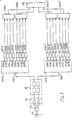
- an electronic surveillance measure (ESM) receiver is shown to include a phased array element 12 which is coupled to a hybrid coupler 14 and which feeds a pair of low noise amplifiers 16.
- ESM electronic surveillance measure
- phased element 12 vertical polarized and horizontal polarized electromagnetic signals are fed through the coupler.
- right-hand circular polarized and left-hand polarized output signals which are amplified by the low noise amplifiers 16 and fed to amplitude and phase control circuit 18.
- the amplitude and phase control circuits which are required are generally a phase shifter and an attenuator. From the output of the phase control and amplitude control circuits 18, the signals are fed to one of a pair of frequency multiplexers 20a, 20b.
- the frequency multiplexers 20a, 20b here shown in block diagram form and will be further described in conjunction with FIG. 2 provide from an input signal fed to terminals 19a, 19b one pair of a plurality of pairs of output signals at terminals 21a-21h and 21a′-21h′ in accordance with the frequency characteristics of the input signal. That is, the frequency multiplexer 20a is used to divide the input signal into a plurality of sub-band signals of left-hand circular-polarization and right-hand circular polarization having selected frequency bandwidths in a manner to be described in conjunction with FIG. 2.
- the outputs 21a-21h from the frequency multiplier 20a and outputs 21a′-21h′ from frequency multiplexer 20b are fed to mixer/amplifier circuits 22a-22h, 22a′-22h′ and such signals are fed by a local oscillator signal LO which provides in combination with the mixer portion of the circuits 22a-22h, 22a′, 22b′ an I.F. frequency signal at the output thereof in a manner which is generally known.
- Frequency multiplexers 20a, 20b are each arranged to provide even and odd sub-bands such that the odd sub-bands are coupled to outputs 21a-21d, 21a′-21d′ and the even sub-bands are coupled to outputs 21e-21h, and 21e′-21h′.
- These output signals are here combined by power combiners 24a, 24b and 24a′, 24b′ and are fed to the receiver processor 26.
- the receiver processor 26 compares signals from the outputs of power combiners 24a-24b and 24a′-24b′.
- Dividing the input signal and combining even and odd sub-band signal components permits the receiver processor 26 to track the input signal through a sub-band and betwen adjacent odd and even sub-bands as long as the filter skirt or "roll-off" characteristics of the frequency multiplexer are well known.
- the outputs from the power combiner 24a and 24b are fed to a receiver processor 26 and determinations are made by the receiver processor on the characteristics of the signals fed thereto in a manner which is generally known.
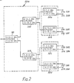
- a first embodiment of an eight channel frequency multiplexer here 20a for use in the receiver in FIG. 1 is shown to include a plurality of here seven diplexer circuits 30, 31a, 31b and 32a-32d.
- the diplexer circuits 30, 31a, 31b and 32a-32d are each chosen to have a pair of passband frequency characteristics.
- the diplexer circuit 30 connected the input of the frequency multiplexer is selected to have a relatively broadband frequency passband characteristic
- the diplexer elements 32a-32d at the outputs 21a-21h of the multiplexer 20a are selected to have relatively narrowband frequency characteristics.
- the ESM receiver has a bandwidth of 6-18 GHz. Accordingly, the input signal fed to terminal 19 of the eight channel multiplexer 20a has a bandwidth of 6-18 GHz. Since eight channels will be provided from the output of each frequency multiplexer 20a, 20b, each one of said channels 21a-21h has a passband of 1.5 GHz. Further, with the arrangement to be described, the odd sub-bands are provided at outputs 21a, 21c, 21e, and 21g and the even sub-bands are provided at outputs 21b, 21d, 21f, and 21h as shown.
- the first diplexer element 30 has a pair of passbands.
- the first passband being over the range of 6-16.5 GHz
- the second passband being over the range of 7.5-18 GHz.
- the first passband is fed to a diplexer 31a and the second passband is fed to a diplexer 31b.
- Diplexer 31a will feed the odd diplexer elements 32a, 32b
- diplexer 31b will feed the even diplexer elements 32c and 32d.
- Diplexer 30 provides a first band comprised of sub-bands corresponding to sub-bands SB1-SB7 (outputs 21a-21g) and is fed to diplexer 31a.
- subband 8 excluded from the first output of diplexer 30 is subband 8.
- Diplexer 31a provides a first signal corresponding to channels or sub-bands SB1-SB3, the second one corresponding to sub-bands SB5-SB7. Dropped at the second diplexer element therefore is sub-band SB4.
- the first odd diplexer 32a provides sub-bands SB1, SB3, and the second odd diplexer 32b provides sub-bands SB5 and SB7.
- dropped or rejected from the first odd sub-band diplexer 32a is sub-band SB2, and dropped from the second odd diplexer is sub-band SB6.
- provided at the outputs 21a, 21c, 21e and 21g of the odd diplexers 32a, 32b are sub-bands SB1, SB3, SB5, and SB7.
- Diplexer 30 also provides the second output including sub-bands SB2-SB8 and thus excluded from the second output from the diplexer 30 is sub-band SB1.
- Sub-bands SB2-SB8 are fed to the diplexer element 31b which provides a first output comprised of sub-bands SB2-SB4 and a second sub-band output comprised of sub-bands SB6-SB8, thus excluded from the second diplexer element 31b is sub-band SB5.
- Diplexer 32c provides passbands corresponding to sub-bands SB2 and SB4 at outputs 21f and 21d, thus excluding sub-band SB3 whereas diplexer 32d provides passbands corresponding to sub-bands SB6 and SB8 at outputs 21f and 21h and thus excludes sub-band SB7. Therefore, at the output of the frequency multiplexer 20a are provided even sub-bands at terminals 21b, 21d, 21f, and 21h and odd sub-bands at terminals 21a, 21c, 21e and 21g.
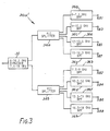
- an alternate embodiment for an eight channel multiplexer is shown to include a diplexer 30 as described in conjunction with FIG. 2, which provides a pair of outputs which fed a pair of 4:1 power splitters 34a-34b, as shown.
- Power splitter 34a feeds bandpass filters 36a, 36c, 36e, and 36g
- power splitter 34b feeds bandpass filters 36b, 36d, 36f, and 36h.
- Each one of the characteristics of the bandpass filters 36a-36h is selected to provide a 1.5GHz wide passbands over the frequencies indicated to provide sub-bands SB1-SB8, as shown.
- diplexers 30, 31a, 31b, and 32a-32d of FIG 2, diplexer 30 and bandpass filters of FIG 3 are here each provided by transversal or recursive filters.
- the diplexers may be provided by using two transversal filters arranged to share a common input line.
- the bandpass filter are either transversal or recursive filters having a bandpass characteristic.
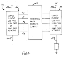
- a generalized block diagram of a transversal filter 40 is shown to include an input network 41 comprised of lumped elements having a selected passband characteristic selected from the group of a low pass filter, a high pass filter, and a bandpass filter characteristic.
- a weighting network 42 comprised of transversal and/or recursive elements is coupled to the input network and is arranged such that successive portions of an input signal fed to the input network are coupled to successive ones of weighting elements of the weighting network.
- the outputs of the weighting network are coupled to an output network comprised of lumped elements having a selected passband characteristic selected from the group of a low pass filter, a high pass filter, and a bandpass filter characteristic.
- the weighting network 42 feeds successive portions of the input signal fed to network 41, each portion having an assigned weight here represented by coefficients A0, A1, A2... A n to the output network 44.
- Each of networks 41 and 44 have a pair of terminals 41a, 41b and 44a, 44b respectively.
- One of each of said pair of terminals provides respectively, the input terminal and output terminal of the transversal filter 40.
- the other one of each of said pair of terminals provides impedance terminations.
- the terminations are preferably open circuits having an infinite impedance or could be others such as a characteristic impedance of the particular network.
- the weighting network 42 is comprised of elements which couple selected portions of the successive signals between the input network and output network.
- the transversal elements which couple from input to output are field effect transistors having a gate electrode as an input and drain electrode as an output.
- Recursive elements which couple from output to input could also be field effect transistors although their use may complicate stability considerations, and are preferable passive components such as resistors.
- the coefficients are determined in accordance with well-known filter theory modified as will be described herein and are provided by varying the size of the transistors (i.e. selecting the gate length). This will provide transistors having various gains and thus weights.
- the values of resistors are selected to provide different weights and in particular may typically range between 50 ⁇ to 2K ⁇ .
- the generalized network shown in FIG. 4 may be constructed to provide any desired passband characteristic.
- the basic shape of the transversal filter response is provided by using lumped element networks 41 and 44 having selected passband characteristics corresponding to the basic shape of the transversal filter response.
- the weighting means are used to improve the response (i.e. provide sharper cut-off or roll-off at the band edges) rather than form the basic shape of the response, as in prior approaches.
- bandpass filter responses will be described in conjunction with FIGS. 5-7 and 5A-7A. Other responses are also possible. For example, low pass or high pass filters having sharp roll-off may be provided.
- Table 1 below provides possible but by no means all choices for networks 41 and 44 to provide a basic passband characteristic to be improved upon by appropriate selection of coefficients A o -A n .
- Each network 41, 44 has a cut-off frequency corresponding to a cut-off frequency of the transversal filter.
- the transversal filters employ lumped element networks having a passband characteristic which is used to define in part the passband characteristic for the transverse filter. This may be further explained in conjunction with FIGS. 5-7 and 5A-7A.
- a first general embodiment of a transversal filter 51′ is shown to include the network 41 comprised of a plurality of series connected inductors L1-L8 and shunt mounted capacitors C1-C4.
- Network 41 is provided as a lumped element, low pass filter terminated in the characteristic impedance in accordance with the characteristic impedance of the network 41, and as a low pass filter provides phase delay to an input signal fed thereto.
- the output network 44 is here comprised of a plurality of series connected capacitors C5-C12 and shunt mounted inductors L9-L12.
- network 44 is a high pass filter which provides a phase advance characteristic to signals propagating thereto.
- transversal elements FET 1 - FET 5 are used to couple selected portions 15 from the input network 41 to the output network 44.
- an input signal is fed to input terminal 41a.
- the input signal has a bandwidth which is greater than the bandwidth of the signal to be coupled from the output of the element at terminal 44a.
- a D.C. blocking capacitor C connected between terminal 41a and the network 41 is used to prevent upset in the D.C. bias characteristics of the transversal elements in network 42.
- the input signal propagates along the network 41 and is delayed by successively increasing increments in phase between each one of the gate electrodes of the transistors FET 1 - FET 5. Thus successive portions of said signal each having successively increasing amount of phase delay are fed through the field effect transistors FET 1 - FET 5.
- the field effect transistors FET 1 - FET 5 each provide selected weighted amplitudes to output signals in response to the input signal.
- the weights are selected in accordance with the desired passband shape of the transversal filter 51′ using well-known transversal theory.
- the basic shape of the filter response i.e. the band pass response
- the selected weight values are provided to the transistors FET 1 - FET 5 by appropriate selection of the gate periphery (i.e. gate length) of each one of the transistors. That is, for a signal which is to be weighted with a relatively high weight value, the periphery of transistor would be a relatively large, to provide such transistor with high gain and output signal amplitude.
- the transversal filter 40 comprises an input line comprised of a low pass filter and an output line comprised of a high pass filter
- the fundamental shape of the bandpass characteristic at the output of the filter is determined in large part by the passband characteristics of the input and the output networks.
- the bandpass characteristic of the transversal filter 51 is provided with very steep slopes by only five transversal elements.
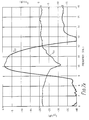
- FIG. 6 A computer simulated design response of the bandpass filter is shown in FIG. 6 having values of inductance and capacitance for the networks 41 and 44 and values for the weight functions for FET 1 - FET 5 is shown.
- Such a circuit was also fabricated using metal electrode semiconductor field effect transistors comprised of suitable dopant gallium arsenide layers supported on a gallium arsenide substrate having a ground plane conductor.
- the measured filter response (
- inductors were implemented by distributed lumped elements that is by sections of microstrip transmission line.
- the numbers next to the inductor elements refers to the width and length of the strip conductor forming the microstrip lines.
- the inductors could have been lumped elements such as spiral inductors. Spiral inductors are generally smaller for a given inductance but are also generally more difficult to model and fabricate than sections of microstrip transmission line.
- FIGS. 6 and 6A correspond to a transversal filter having a pass band of 10.3 GHz to 14.8 GHz.
- FIGS. 7 and 7A a second design example generally as fabricated above for FIG. 6 is shown having element values as indicated. This is a 9.8 GHz to 11.16 GHz band pass transversal filter. The measured response is shown in FIG. 7A.
- the transversal filter 40′ includes an input network 41′ here comprised of a plurality of series connected capacitors (not referenced) and shunt mounted inductors (not referenced) which provide in combination a phase advance or high pass filter network, and network 44′ includes a plurality of of series connected inductors (not referenced) and shunt mounted capacitors (not referenced), as shown, which provides here a phase delay or a low pass filter network.
- Network 41′ and 44′ are connected together by a plurality of transversal elements 42 as generally described in conjunction with FIG. 5. The output is taken at terminal 44b of the network 44′ and terminal 44a thereof is terminated in an impedance.
- a generalized block diagram of a diplexer 55 here having a pair of transversal filter element sets 50a, 50b, is shown to include a lumped element propagation network 41, here said lumped element network 41 comprised of low pass (i.e. phase delay), high pass (i.e. phase advance) or band pass circuit elements.
- Lumped element network 41 has an input terminal 41a and an second terminal 41b which is terminated in any impedance such as an infinite impedance which does not absorb power or possible the characteristic impedance of the lumped element network 41.
- the diplexer 55 further includes a pair of output lumped element networks 44 and 48.
- each one of the said output networks are also lumped element networks and are comprised of high pass (i.e.
- phase advance low pass (i.e. phase delay) or band pass networks.
- the input network is either a phase delay or advance network
- one of the output networks is a phase advance network and the other is a phase delay network.
- Input network 41 is coupled to the output network 44 by a first network 42 of transversal and/or recursive elements, and the input network 41 is also coupled to output network 48 through a second network 46 of transversal and/or recursive elements.
- each one of the networks of transversal and/or recursive elements 42, 46 are comprised field effect transistors having gate, drain, and source electrodes. Preferable, however, recursive elements are provided by resistors as described above.
- Transversal elements are provided by coupling the signal from the input network to the output network, that is by coupling the gate electrode to the input network and having the drain electrode feed the output network 44, for example.
- Recursive elements are feedback elements and thus have the gate electrode coupled to the output network 44 and have the drain electrodes coupled to feed the input network 41 or alternatively could by a resistor.
- the transversal and/or recursive elements therefore, provide weighting factors A o -A n to the signals coupled to the output network 44 and weighting signals A o ′-A n ′ to the lumped element network 48.
- diplexer 55 is here comprised of a pair of transversal and/or recursive filter sets 50a-50b sharing a common input network line.
- the characteristic of each one of the transversal/recursive filters 50a-50b are selected to provide a one of a pair of selected passbands at a selected one of the terminals 44a, 44b of network 44 and terminal 48a, 48b of network 48. That is, one of said terminals 44a, 44b and 48a, 48b of each network 44, 48 is generally terminated in a characteristic impedance in accordance with the characteristic impedance of the lumped element network 44 and 48, and a second one of said terminals provides the output for the networks 44 and 48.
- the output of the network is adjacent to the input terminal of the network and thus, terminal 44a and 48a would be provided as the outputs of the filter when the input terminal of the filter was terminal 41a.
- the outputs may also be provided at terminals 44b and terminals 48b. The differences in electrical pathlengths through each of the elements would necessarily have to be taken into consideration in order to change the location of the output terminal.
- a diplexer 55 is shown to include a pair of transversal filters sets 50a-50b, having the general characteristics of the transversal filter 40 (FIG. 5)
- Diplexer 55 includes the lumped element filter network 41 as generally described in conjunction with FIG. 5 which has a first terminal 41a providing the input terminal for the network 55 and a second terminal 41b which is terminated in impedance as mentioned above.
- a pair of output networks 44 and 48 are also provided.
- network 44 is similar to that described in conjunction with FIG. 5 for transversal element 40.
- network 48 is a phase delay network, except that the passband of network 48 is different from that of network 44.
- the diplexer element 30 has a input network 41 having a passband characteristic of 6-18 GHz and has a network 44 having a passband of 6-16 GHz and network 48 having a passband of 7.5-18 GHz.
- the selected frequency passband characteristics are provided to the circuits.
- the values of the weighting factors provided to each one of the transversal elements of networks 42 and 46 a transversal filter response having selected passband characteristics with steep frequency slopes without harmonic passbands is provided at each one of the outputs of the diplexer 40.
- Recursive filter 60 is similar to transversal filter shown in FIG. 5, except that the second transversal element is replaced by a recursive element here resistor RR2, which is coupled between output network 44 and input network 41, as shown.
- the third transversal element is omitted.
- element RR2 feedbacks a portion of the output signal back to the input of the recursive filter.
- the use of one or more recursive elements in the general lumped element distributed filters as described may provide a further improvement in performance or size reduction compared to the transversal filters, as described above.
- the direction of the output port can be either direction depending on the choice of the delays, t a and t b .
- Phase delays t a and t b are chosen to be the same in travelling wave amplifiers in order to combine the power from all the FETs in phase at the output port. This situation can be illustrated as RF signals travelling through two different paths, a and b. It can be shown easily that the transfer characteristic of this type of circuit has very little frequency dependence, and yields an excellent broadband circuit. However, a sharp cut-off characteristic is difficult to achieve.
- a transversal filter of the present invention includes lumped element low pass, high pass, and/or bandpass input and output lines having band edges or cutoff frequencies corresponding to that of the filter.
- a bandpass filter could include both low pass (phase delay) and high pass(phase advance) lines. With opposite phase shifts, when combined the lines provide a strong frequency dependent behavior requiring a relatively small number of elements to provide steep frequency slopes.
- the circuit now has a bandpass characteristic rather than the low pass characteristic of conventional transversal filters.
- phase delay line is an ordinary piece of transmission line and a phase advance line is a piece of a transmission line of negative length.
- Both lines can be simulated by a lumped element ladder circuit using Ls and Cs.
- a phase advance line is provided and if the same values for Cs and Ls are used, the line impedance is identical and the propagation constant is the reverse of the other with opposite sign.
- Its response curve can be designed to any classical filter characteristics such as Tchebyschev or Maximally flat, by choosing a i , as before.
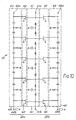
- a generalized topology of a recursive filter as illustrated in FIG.11 includes a mix of feed forward paths and feed back paths.
- the transfer function of a circuit with M + 1 feed forward paths and N feed back paths can be written in the form;
- delay and advance line sections will provide a compact version of this circuit.
- Multiple active elements and feedback paths should improve the cut-off characteristics also.
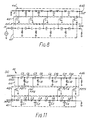
- the position of the output port in FIG. 5 can be brought to the other end of the output line (as shown in FIG. 8) and the circuit can be designed to combine the output power from the FETs at the output port in a travelling-wave manner.
- the configuration is similar to the conventional travelling wave amplifier because, in the passband, the power is added in phase at the output port in a similar manner. However, the power is rejected outside the band due to the difference of frequency sensitivity of phase shift between the input and output lines.
- a power response equation similar to Eq. 16 can be derived for this circuit, indicating the same filtering function is possible.
- the circuit has lumped element phase delay lines in the input line and lumped element phase advance lines in the output lines.
- the spurious passbands are also suppressed with this topology. This is explained as follows. Lumped element expression of a transmission line, both delay and advance, is not allowed near the cut-off frequency.
- the lumped circuit expression of a delay line represents a low pass filter and beyond the cut-off frequency, the characteristic impedance of the line becomes imaginary and wave propagation stops. This does not occur with the transmission line model.
- the lumped circuit for the phase advance line is a high pass filter and wave propagation stops below the cut-off frequency.
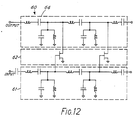
- a transversal filter 60 having input and output propagation media 61 and 64 provided as lumped element lines L's and C's having a bandpass characteristic is shown.
- Each of the lines 61, 64 has frequency skirts or cutoff frequencies corresponding to those of the transversal filter 60 to provide such a filter having very sharp frequency roll-off at the band edges with a mininum number of transversal elements 62, as with the other embodiments described above.
Landscapes
- Filters That Use Time-Delay Elements (AREA)
- Networks Using Active Elements (AREA)
- Cable Transmission Systems, Equalization Of Radio And Reduction Of Echo (AREA)
Applications Claiming Priority (2)
| Application Number | Priority Date | Filing Date | Title |
|---|---|---|---|
| US292712 | 1989-01-03 | ||
| US07/292,712 US5021756A (en) | 1989-01-03 | 1989-01-03 | Transversal and recursive filters useable in a diplexer |
Publications (3)
| Publication Number | Publication Date |
|---|---|
| EP0377300A2 true EP0377300A2 (fr) | 1990-07-11 |
| EP0377300A3 EP0377300A3 (fr) | 1991-01-02 |
| EP0377300B1 EP0377300B1 (fr) | 1995-02-22 |
Family
ID=23125872
Family Applications (1)
| Application Number | Title | Priority Date | Filing Date |
|---|---|---|---|
| EP89313332A Expired - Lifetime EP0377300B1 (fr) | 1989-01-03 | 1989-12-20 | Filtres transversaux et récursifs |
Country Status (4)
| Country | Link |
|---|---|
| US (1) | US5021756A (fr) |
| EP (1) | EP0377300B1 (fr) |
| JP (1) | JPH0767061B2 (fr) |
| DE (1) | DE68921330T2 (fr) |
Cited By (3)
| Publication number | Priority date | Publication date | Assignee | Title |
|---|---|---|---|---|
| EP1615340A1 (fr) * | 2004-07-09 | 2006-01-11 | Alcatel | Procédé de réalisation d'un circuit électronique avec fonction de transfer desirée et arrangement obtenu selon ce procédé |
| EP1347573A4 (fr) * | 2000-12-22 | 2008-05-21 | Ube Industries | Multiplexeur |
| EP2399321A4 (fr) * | 2009-02-18 | 2015-02-11 | Hollinworth Fund L L C | Systèmes amplificateurs de puissance à méta-matériau |
Families Citing this family (21)
| Publication number | Priority date | Publication date | Assignee | Title |
|---|---|---|---|---|
| US5021756A (en) | 1989-01-03 | 1991-06-04 | Raytheon Company | Transversal and recursive filters useable in a diplexer |
| US5229729A (en) * | 1989-12-14 | 1993-07-20 | Murata Manufacturing Co., Ltd. | Radio frequency signal combining/sorting apparatus |
| US5168250A (en) * | 1991-06-17 | 1992-12-01 | E-Systems, Inc. | Broadband phase shifter and vector modulator |
| US5339057A (en) * | 1993-02-26 | 1994-08-16 | The United States Of America As Represented By The Secretary Of The Navy | Limited bandwidth microwave filter |
| WO1996012351A1 (fr) * | 1994-10-17 | 1996-04-25 | Scientific-Atlanta, Inc. | Diplexeur pour filtre |
| US5815804A (en) * | 1997-04-17 | 1998-09-29 | Motorola | Dual-band filter network |
| US6680978B1 (en) * | 1999-03-01 | 2004-01-20 | Adtran, Inc. | Method and apparatus for nonlinear filtering and controlling the peak-to-average ratio |
| US6636128B2 (en) * | 2001-06-07 | 2003-10-21 | The United States Of America As Represented By The Secretary Of The Navy | Frequency-tunable notch filter |
| US7656909B1 (en) * | 2003-05-05 | 2010-02-02 | Rockwell Collins, Inc. | Self-steering autoplexer for transmitter multicoupling |
| US7142596B2 (en) * | 2004-06-17 | 2006-11-28 | Vitesse Semiconductor Corporation | Integrated circuit implementation for power and area efficient adaptive equalization |
| US7346645B2 (en) * | 2004-11-05 | 2008-03-18 | International Business Machines Corporation | Architecture for transverse-form analog finite-impulse-response filter |
| US7606184B2 (en) * | 2005-01-04 | 2009-10-20 | Tdk Corporation | Multiplexers employing bandpass-filter architectures |
| DE102005046445B4 (de) * | 2005-09-28 | 2019-10-10 | Snaptrack, Inc. | Bandpassfilter |
| WO2008029643A1 (fr) | 2006-08-31 | 2008-03-13 | Nec Corporation | Circuit de filtre d'égalisation |
| US8483318B2 (en) * | 2008-11-04 | 2013-07-09 | Agilent Technologies, Inc. | Split band signal processing |
| EP2392135A1 (fr) * | 2009-02-02 | 2011-12-07 | Technetix Group Limited | Dispositif de division de signaux |
| KR101572534B1 (ko) * | 2009-06-18 | 2015-11-30 | 삼성전자주식회사 | Rf 프론트 앤드 모듈 및 이를 이용한 멀티밴드 통신 모듈 |
| KR101565995B1 (ko) * | 2009-07-16 | 2015-11-05 | 삼성전자주식회사 | 듀얼-입력 듀얼-출력의 필터를 이용한 멀티-대역의 라디오 주파수 신호 송수신 시스템 |
| US8912847B2 (en) | 2009-12-03 | 2014-12-16 | Epcos Ag | Power amplifier circuit and front end circuit |
| PL2898565T3 (pl) * | 2012-09-18 | 2018-12-31 | Aselsan Elektronik Sanayi Ve Ticaret Anonim Sirketi | Przełączany multiplekser |
| JP6362363B2 (ja) * | 2014-03-10 | 2018-07-25 | キヤノン株式会社 | 画像推定方法、プログラム、記録媒体および画像推定装置 |
Family Cites Families (11)
| Publication number | Priority date | Publication date | Assignee | Title |
|---|---|---|---|---|
| US2790956A (en) * | 1953-07-09 | 1957-04-30 | Bell Telephone Labor Inc | Distortion corrector |
| US3611201A (en) | 1969-10-21 | 1971-10-05 | Bell Telephone Labor Inc | Carrier transversal equalizer |
| JPS4965755A (fr) * | 1972-10-26 | 1974-06-26 | ||
| US4238744A (en) * | 1977-09-08 | 1980-12-09 | Victor Company Of Japan, Ltd. | Frequency band dividing filter using delay-line filter |
| FR2443765A1 (fr) * | 1978-12-05 | 1980-07-04 | Thomson Csf | Amplificateur distribue pour hyperfrequences et dispositif d'amplification comportant un tel amplificateur |
| US4291286A (en) * | 1979-12-17 | 1981-09-22 | Ford Aerospace & Communications Corporation | High bandwidth transversal filter |
| US4751744A (en) * | 1985-05-28 | 1988-06-14 | Texas Instruments Incorporated | Monolithic distributed mixer |
| US4661789A (en) * | 1985-07-17 | 1987-04-28 | The United States Of America As Represented By The Secretary Of The Navy | Microwave recursive filter |
| US4918401A (en) * | 1985-09-30 | 1990-04-17 | Siemens Aktiengesellschaft | Step adjustable distributed amplifier network structure |
| US4772858A (en) * | 1987-11-04 | 1988-09-20 | Raytheon Company | Distributed amplifying switch/rf combiner |
| US5021756A (en) | 1989-01-03 | 1991-06-04 | Raytheon Company | Transversal and recursive filters useable in a diplexer |
-
1989
- 1989-01-03 US US07/292,712 patent/US5021756A/en not_active Expired - Lifetime
- 1989-12-20 DE DE68921330T patent/DE68921330T2/de not_active Expired - Lifetime
- 1989-12-20 EP EP89313332A patent/EP0377300B1/fr not_active Expired - Lifetime
-
1990
- 1990-01-04 JP JP2000203A patent/JPH0767061B2/ja not_active Expired - Lifetime
Cited By (3)
| Publication number | Priority date | Publication date | Assignee | Title |
|---|---|---|---|---|
| EP1347573A4 (fr) * | 2000-12-22 | 2008-05-21 | Ube Industries | Multiplexeur |
| EP1615340A1 (fr) * | 2004-07-09 | 2006-01-11 | Alcatel | Procédé de réalisation d'un circuit électronique avec fonction de transfer desirée et arrangement obtenu selon ce procédé |
| EP2399321A4 (fr) * | 2009-02-18 | 2015-02-11 | Hollinworth Fund L L C | Systèmes amplificateurs de puissance à méta-matériau |
Also Published As
| Publication number | Publication date |
|---|---|
| DE68921330T2 (de) | 1995-10-19 |
| EP0377300B1 (fr) | 1995-02-22 |
| DE68921330D1 (de) | 1995-03-30 |
| EP0377300A3 (fr) | 1991-01-02 |
| JPH0767061B2 (ja) | 1995-07-19 |
| JPH02228115A (ja) | 1990-09-11 |
| US5021756A (en) | 1991-06-04 |
Similar Documents
| Publication | Publication Date | Title |
|---|---|---|
| EP0377300B1 (fr) | Filtres transversaux et récursifs | |
| US5039891A (en) | Planar broadband FET balun | |
| US9449749B2 (en) | Signal handling apparatus for radio frequency circuits | |
| CA1341457C (fr) | Circuit melangeur | |
| US6636128B2 (en) | Frequency-tunable notch filter | |
| US7676252B2 (en) | Filter circuit having plural resonator blocks with a phase adjustment unit | |
| EP0308479B1 (fr) | Reseau dephaseur de microondes monolithiques avec des sorties multiples entre lesquelles une difference de phase constante est maintenue sur une large gamme de frequences | |
| EP0403176B1 (fr) | Dephaseur analogue continûment variable | |
| US4885562A (en) | Microwave delay circuit having a bridge-T circuit | |
| US5832376A (en) | Coplanar mixer assembly | |
| US6492886B1 (en) | Laminated filter, duplexer, and mobile communication apparatus using the same | |
| US4662000A (en) | Frequency conversion circuits | |
| CN117938116A (zh) | 一种带斜率控制的数控衰减器 | |
| US5977843A (en) | High frequency power divider and high frequency power combiner | |
| US4661789A (en) | Microwave recursive filter | |
| EP4466790B1 (fr) | Déphaseur actif à large bande à faible bruit en cascade | |
| US12424724B2 (en) | Quadrature couplers and methods of operation | |
| US5323064A (en) | Radio frequency signal frequency converter | |
| EP1496528A2 (fr) | Condensateur différentiel, élément d'antenne différentiel et résonateur différentiel | |
| US4525680A (en) | Microwave/millimeter wave amplifier with RF feedback | |
| EP0430509A2 (fr) | Amplificateur bidirectionnel symétrique | |
| US4118672A (en) | Attenuation equalizer having constant resistance | |
| RU2060571C1 (ru) | Частотный разделитель на коаксиальных диэлектрических резонаторах | |
| WO2001097321A1 (fr) | Filtre coupe-bande accordable en frequence | |
| Brucher et al. | Broadband and tunable negative monolithic circuits for microwave active filters compensation |
Legal Events
| Date | Code | Title | Description |
|---|---|---|---|
| PUAI | Public reference made under article 153(3) epc to a published international application that has entered the european phase |
Free format text: ORIGINAL CODE: 0009012 |
|
| AK | Designated contracting states |
Kind code of ref document: A2 Designated state(s): DE FR GB |
|
| PUAL | Search report despatched |
Free format text: ORIGINAL CODE: 0009013 |
|
| AK | Designated contracting states |
Kind code of ref document: A3 Designated state(s): DE FR GB |
|
| 17P | Request for examination filed |
Effective date: 19910621 |
|
| 17Q | First examination report despatched |
Effective date: 19930921 |
|
| GRAA | (expected) grant |
Free format text: ORIGINAL CODE: 0009210 |
|
| AK | Designated contracting states |
Kind code of ref document: B1 Designated state(s): DE FR GB |
|
| REF | Corresponds to: |
Ref document number: 68921330 Country of ref document: DE Date of ref document: 19950330 |
|
| ET | Fr: translation filed | ||
| PLBE | No opposition filed within time limit |
Free format text: ORIGINAL CODE: 0009261 |
|
| STAA | Information on the status of an ep patent application or granted ep patent |
Free format text: STATUS: NO OPPOSITION FILED WITHIN TIME LIMIT |
|
| 26N | No opposition filed | ||
| PGFP | Annual fee paid to national office [announced via postgrant information from national office to epo] |
Ref country code: GB Payment date: 19981203 Year of fee payment: 10 |
|
| PG25 | Lapsed in a contracting state [announced via postgrant information from national office to epo] |
Ref country code: GB Free format text: LAPSE BECAUSE OF NON-PAYMENT OF DUE FEES Effective date: 19991220 |
|
| GBPC | Gb: european patent ceased through non-payment of renewal fee |
Effective date: 19991220 |
|
| PGFP | Annual fee paid to national office [announced via postgrant information from national office to epo] |
Ref country code: FR Payment date: 20081110 Year of fee payment: 20 |
|
| PGFP | Annual fee paid to national office [announced via postgrant information from national office to epo] |
Ref country code: DE Payment date: 20081128 Year of fee payment: 20 |