EP0377886A2 - Montage pour le transfert de mots de données subdivisés en plusieurs parties - Google Patents
Montage pour le transfert de mots de données subdivisés en plusieurs parties Download PDFInfo
- Publication number
- EP0377886A2 EP0377886A2 EP89123790A EP89123790A EP0377886A2 EP 0377886 A2 EP0377886 A2 EP 0377886A2 EP 89123790 A EP89123790 A EP 89123790A EP 89123790 A EP89123790 A EP 89123790A EP 0377886 A2 EP0377886 A2 EP 0377886A2
- Authority
- EP
- European Patent Office
- Prior art keywords
- control unit
- data
- words
- buffer memory
- masking
- Prior art date
- Legal status (The legal status is an assumption and is not a legal conclusion. Google has not performed a legal analysis and makes no representation as to the accuracy of the status listed.)
- Granted
Links
Images
Classifications
-
- G—PHYSICS
- G06—COMPUTING OR CALCULATING; COUNTING
- G06F—ELECTRIC DIGITAL DATA PROCESSING
- G06F5/00—Methods or arrangements for data conversion without changing the order or content of the data handled
- G06F5/06—Methods or arrangements for data conversion without changing the order or content of the data handled for changing the speed of data flow, i.e. speed regularising or timing, e.g. delay lines, FIFO buffers; over- or underrun control therefor
- G06F5/10—Methods or arrangements for data conversion without changing the order or content of the data handled for changing the speed of data flow, i.e. speed regularising or timing, e.g. delay lines, FIFO buffers; over- or underrun control therefor having a sequence of storage locations each being individually accessible for both enqueue and dequeue operations, e.g. using random access memory
-
- G—PHYSICS
- G06—COMPUTING OR CALCULATING; COUNTING
- G06F—ELECTRIC DIGITAL DATA PROCESSING
- G06F2205/00—Indexing scheme relating to group G06F5/00; Methods or arrangements for data conversion without changing the order or content of the data handled
- G06F2205/10—Indexing scheme relating to groups G06F5/10 - G06F5/14
- G06F2205/108—Reading or writing the data blockwise, e.g. using an extra end-of-block pointer
Definitions
- the invention relates to an arrangement for transmitting data words divided into several parts (partial words) between two control units according to the preamble of claim 1.
- Control units that work with different data word widths are often used in data processing systems. For example, it occurs in automation systems that the data from signal formers, such as analog-to-digital converters, digital-to-analog converters, timers, counters and the like, have a word length which is greater than that with which the processing central processor works. A single word of such signal formers can occupy four bytes, whereas the internal processing width of the central processing unit is limited to two bytes.
- the transmission line between the central processor and the signal shaper is dimensioned so that the data words are not divided as a whole, but divided, e.g. B. byte by byte must be transferred.
- this problem occurs when adapting the interface of different devices that work at different speeds and / or word widths and in which data words are transmitted in a divided manner.
- buffer memories are used, in which transmission controllers write and read the data to be transmitted. It can then occur that one control unit has only partially written a word and the other control unit then calls up the entire word before the first unit was able to write the word completely. The second control unit then receives a falsified word.
- an error occurs if one control unit calls up a first word part from a memory area of the buffer memory and the other unit enters a complete word into the same memory area before the first controller transfers the second word can retrieve part.
- This difficulty could be remedied in that a word is only declared valid when the number of accesses multiplied by the partial word width equals the total word width.
- this method is unsuitable if the word width is variable. It is also possible to provide information that belongs together with an identifier. If information that does not belong together is then transmitted, an evaluation logic located in the receiving unit detects the error. This method has the disadvantage that additional information must be transmitted and that the evaluation in each individual data terminal, for. B. signal shaper must be done.
- the present invention has for its object to provide an arrangement of the type specified in the preamble of claim 1, which can be easily adjusted to data words of different widths.
- the new arrangement is suitable for transferring data between two or more units, one controlling the access of the other units to the buffer memory.
- a preferred application are bus systems, e.g. B. process control and control systems with a system bus over which data is transmitted between peripheral units and one or more central processors.
- Peripheral units are e.g. B. analog-to-digital converter, digital-to-analog converter, position controls, display modules and the like.
- the buffer memory then establishes the connection between the system bus and the internal bus of the peripheral units.
- the masking code can be changed without changing the arrangement, so it is easily adjustable.
- the controls of different devices can have the same structure. It is therefore also possible to send and receive data of different word widths with the same control unit, by resetting the masking code from one data transmission to the next.
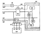
- STE is a control unit of a peripheral device between which and another control unit, not shown, z. B. a central processor, data to be transmitted.
- the units are part of a data processing system, e.g. B. a process control system in which the peripheral units can be analog-to-digital converters, digital-to-analog converters, display units and the like.
- a system bus establishes the connection between the units. It contains SDT system data lines via which partial words of the data words to be transmitted are transmitted. Control data are transmitted via system control lines SST and buffer memory addresses via system address lines SAD.
- the word length of the data transmitted from or to the peripheral units differs depending on the type of peripheral unit, and its clock frequency can also be different.
- a buffer memory PSP expediently a so-called dual-port RAM, is provided, which is connected on the one hand to the system bus and on the other hand to the internal bus of the peripheral control unit.
- the central processor issues log. "1" signal on a line SRD, in the case of a read command on a line SWR.
- the signals on the lines SRD, SWR are fed to an OR gate OR, to the output of which an input U of a register REG is connected. If one of the two signals is log. "1", this is reported by the register REG to the control unit STE via a line SYZ.
- the respective address of the buffer memory transmitted via the system address lines SAD is entered in a register REG.
- the control unit STE wants to write or read a data word into the buffer memory PSP, it first checks whether it accesses the same address area as the central processor.
- the address area comprises such a number of addresses as are required to hold the partial words of a data word.
- the address contained in the register REG is linked in a masking circuit MS1 with a masking code which is entered in a mask register MR.
- the address generated in the peripheral unit with which the buffer memory PSP is to be accessed is linked to the masking code in a masking circuit MS2.
- a comparator VGL checks whether the masking results match.
- the switch US then remains in the position shown in dashed lines in the figure, in which the data inputs and outputs DEA, the address inputs AE and the control inputs SE of the buffer memory PSP are connected to the system bus.
- the signal on the SRD or SWR line, and thus the signal on the SYZ line is withdrawn, and the peripheral control unit STE can access the buffer memory PSP by switching over the switch US.
- the central processor wants to access the buffer memory PSP while the peripheral unit has access, the addresses with which it is accessed are also masked and the results are compared with one another. If these are the same, access is blocked for the central processor, which then tries to access again after a predetermined time. If the comparator determines that the central processor and the peripheral unit access different memory areas, both are given access simultaneously. Simultaneous access means that one unit can enter or read a partial word even if the other unit has not yet completed the transmission of the entire data word. Simultaneous access does not need to be prevented if both units want to read a data word from the buffer memory.
- a major advantage of the new arrangement is that although the data word widths are different for different peripheral units, the same arrangement can be used and that only the masking code has to be adapted to the respective data word width. You can even process data words of different widths with the same control unit. However, this requires that the control unit knows the width of the incoming data word. This can be achieved by assigning a certain buffer memory area to each data word width. The assignment can be stored in a read-only memory. The mask register is then no longer required. The addresses for the buffer memory generated by the control unit are fed to the read-only memory, which thereupon outputs the associated masking code contained in the addressed cell to the two masking circuits MS1, MS2.
Landscapes
- Engineering & Computer Science (AREA)
- Theoretical Computer Science (AREA)
- Physics & Mathematics (AREA)
- General Engineering & Computer Science (AREA)
- General Physics & Mathematics (AREA)
- Communication Control (AREA)
- Bus Control (AREA)
- Techniques For Improving Reliability Of Storages (AREA)
Applications Claiming Priority (2)
| Application Number | Priority Date | Filing Date | Title |
|---|---|---|---|
| DE3900792 | 1989-01-12 | ||
| DE3900792A DE3900792A1 (de) | 1989-01-12 | 1989-01-12 | Anordnung zum uebertragen von in mehrere teile unterteilten datenwoertern |
Publications (3)
| Publication Number | Publication Date |
|---|---|
| EP0377886A2 true EP0377886A2 (fr) | 1990-07-18 |
| EP0377886A3 EP0377886A3 (fr) | 1992-06-24 |
| EP0377886B1 EP0377886B1 (fr) | 1996-03-20 |
Family
ID=6371979
Family Applications (1)
| Application Number | Title | Priority Date | Filing Date |
|---|---|---|---|
| EP89123790A Expired - Lifetime EP0377886B1 (fr) | 1989-01-12 | 1989-12-22 | Montage pour le transfert de mots de données subdivisés en plusieurs parties |
Country Status (4)
| Country | Link |
|---|---|
| EP (1) | EP0377886B1 (fr) |
| AT (1) | ATE135832T1 (fr) |
| DE (2) | DE3900792A1 (fr) |
| ES (1) | ES2083965T3 (fr) |
Cited By (2)
| Publication number | Priority date | Publication date | Assignee | Title |
|---|---|---|---|---|
| DE19909081C2 (de) * | 1999-03-02 | 2003-03-20 | Siemens Ag | Anordnung zur Übertragung von in mehrere Wörter unterteilten Datensätzen |
| DE102011079683A1 (de) * | 2010-08-03 | 2012-06-14 | Continental Teves Ag & Co. Ohg | Dreistufige Speicheranordnung |
-
1989
- 1989-01-12 DE DE3900792A patent/DE3900792A1/de not_active Withdrawn
- 1989-12-22 ES ES89123790T patent/ES2083965T3/es not_active Expired - Lifetime
- 1989-12-22 EP EP89123790A patent/EP0377886B1/fr not_active Expired - Lifetime
- 1989-12-22 DE DE58909627T patent/DE58909627D1/de not_active Expired - Fee Related
- 1989-12-22 AT AT89123790T patent/ATE135832T1/de not_active IP Right Cessation
Cited By (5)
| Publication number | Priority date | Publication date | Assignee | Title |
|---|---|---|---|---|
| DE19909081C2 (de) * | 1999-03-02 | 2003-03-20 | Siemens Ag | Anordnung zur Übertragung von in mehrere Wörter unterteilten Datensätzen |
| DE102011079683A1 (de) * | 2010-08-03 | 2012-06-14 | Continental Teves Ag & Co. Ohg | Dreistufige Speicheranordnung |
| CN103154835A (zh) * | 2010-08-03 | 2013-06-12 | 大陆-特韦斯贸易合伙股份公司及两合公司 | 三级存储器装置 |
| CN103154835B (zh) * | 2010-08-03 | 2016-03-23 | 大陆-特韦斯贸易合伙股份公司及两合公司 | 三级存储器装置及其在机动车中的使用 |
| US10282320B2 (en) | 2010-08-03 | 2019-05-07 | Continental Teves Ag & Co. Ohg | Three-stage memory arrangement |
Also Published As
| Publication number | Publication date |
|---|---|
| EP0377886B1 (fr) | 1996-03-20 |
| DE58909627D1 (de) | 1996-04-25 |
| EP0377886A3 (fr) | 1992-06-24 |
| ATE135832T1 (de) | 1996-04-15 |
| ES2083965T3 (es) | 1996-05-01 |
| DE3900792A1 (de) | 1990-07-19 |
Similar Documents
| Publication | Publication Date | Title |
|---|---|---|
| DE2641741C2 (de) | Rechenanlage aus mehreren miteinander über ein Sammelleitungssystem verbundenen und zusammenwirkenden Einzelrechnern und einem Steuerrechner | |
| DE3300262C2 (fr) | ||
| DE3224034C2 (fr) | ||
| DE3300261C2 (fr) | ||
| DE2455803C2 (de) | Mehrprozessor-Datenverarbeitungsanlage | |
| DE3300263C2 (fr) | ||
| DE1299145B (de) | Schaltungsanordnung zum Steuern von peripheren Ein- und Ausgabegeraeten von Datenverarbeitungssystemen | |
| DE3137627C1 (de) | Anordnung zur schnellen Nachrichtenuebertragung zwischen Rechnern | |
| DE2523372B2 (de) | Eingabe-ZAusgabe-Anschlußsteuereinrichtung | |
| EP0014850A1 (fr) | Dispositif pour étendre le jeu normal de makro-instructions dans un système de traitement d'information | |
| EP0062141B1 (fr) | Circuit pour l'entrée de signaux de commande d'exécution dans un système de micro-ordinateur | |
| DE68924109T2 (de) | Verfahren und System für die Überwachung der Anzahl von freien Puffern. | |
| WO1989003142A1 (fr) | Procede et dispositif de mesure pour l'analyse de perturbations de bus digitaux | |
| WO1996016366A1 (fr) | Configuration a unites maitresses et asservies | |
| DE2100443C3 (de) | Einrichtung zum Prüfen einer logischen Funktionsschaltung in einer Adapter-Steuereinheit einer Datenverarbeitungsanlage | |
| EP0377886B1 (fr) | Montage pour le transfert de mots de données subdivisés en plusieurs parties | |
| DE2242279C3 (de) | Schaltungsanordnung zur Ermittlung von Fehlern in einer Speichereinheit eines programmgesteuerten Datenvermittlungssystems | |
| EP0009625A2 (fr) | Commutateur de transfert de données à l'aide d'une sélection associative d'adresse dans une mémoire virtuelle | |
| DD142135A3 (de) | Mehrrechnerkopplung | |
| DE69110192T2 (de) | Vermittlungsmodul digitaler Datenpakete zur Zuweisung leerer Pakete an einen Koppelpunkt. | |
| DE3325791C2 (de) | Schaltungsanordnung für mit einer zentralen Steuereinrichtung zusammenarbeitende periphere Einheiten | |
| DE3110576A1 (de) | Schaltungsanordnung mit zwei mikrocomputern, die ueber einen bus-koppler miteinander verbunden sind | |
| DE2837709C2 (de) | Schaltungsanordnung zur Behandlung von Teilwörtern in Rechnersystemen | |
| DE2555329C3 (de) | Steuereinrichtung aus mehreren Bausteinen für eine Vermittlungsanlage, insbesondere Fernsprechvermittlungsanlage, und Verfahren zum Betrieb der Steuereinrichtung | |
| DE1449567C3 (de) | Digitales Datenverarbeitungssystem |
Legal Events
| Date | Code | Title | Description |
|---|---|---|---|
| PUAI | Public reference made under article 153(3) epc to a published international application that has entered the european phase |
Free format text: ORIGINAL CODE: 0009012 |
|
| AK | Designated contracting states |
Kind code of ref document: A2 Designated state(s): AT CH DE ES FR GB IT LI SE |
|
| 17P | Request for examination filed |
Effective date: 19901205 |
|
| PUAL | Search report despatched |
Free format text: ORIGINAL CODE: 0009013 |
|
| AK | Designated contracting states |
Kind code of ref document: A3 Designated state(s): AT CH DE ES FR GB IT LI SE |
|
| 17Q | First examination report despatched |
Effective date: 19940927 |
|
| GRAA | (expected) grant |
Free format text: ORIGINAL CODE: 0009210 |
|
| AK | Designated contracting states |
Kind code of ref document: B1 Designated state(s): AT CH DE ES FR GB IT LI SE |
|
| REF | Corresponds to: |
Ref document number: 135832 Country of ref document: AT Date of ref document: 19960415 Kind code of ref document: T |
|
| REG | Reference to a national code |
Ref country code: CH Ref legal event code: NV Representative=s name: SIEMENS SCHWEIZ AG |
|
| REF | Corresponds to: |
Ref document number: 58909627 Country of ref document: DE Date of ref document: 19960425 |
|
| REG | Reference to a national code |
Ref country code: ES Ref legal event code: FG2A Ref document number: 2083965 Country of ref document: ES Kind code of ref document: T3 |
|
| GBT | Gb: translation of ep patent filed (gb section 77(6)(a)/1977) |
Effective date: 19960502 |
|
| ITF | It: translation for a ep patent filed | ||
| ET | Fr: translation filed | ||
| GRAH | Despatch of communication of intention to grant a patent |
Free format text: ORIGINAL CODE: EPIDOS IGRA |
|
| PGFP | Annual fee paid to national office [announced via postgrant information from national office to epo] |
Ref country code: AT Payment date: 19961127 Year of fee payment: 8 |
|
| PGFP | Annual fee paid to national office [announced via postgrant information from national office to epo] |
Ref country code: SE Payment date: 19961210 Year of fee payment: 8 |
|
| PGFP | Annual fee paid to national office [announced via postgrant information from national office to epo] |
Ref country code: ES Payment date: 19961212 Year of fee payment: 8 |
|
| PLBE | No opposition filed within time limit |
Free format text: ORIGINAL CODE: 0009261 |
|
| STAA | Information on the status of an ep patent application or granted ep patent |
Free format text: STATUS: NO OPPOSITION FILED WITHIN TIME LIMIT |
|
| 26N | No opposition filed | ||
| PGFP | Annual fee paid to national office [announced via postgrant information from national office to epo] |
Ref country code: CH Payment date: 19970319 Year of fee payment: 8 |
|
| PGFP | Annual fee paid to national office [announced via postgrant information from national office to epo] |
Ref country code: GB Payment date: 19971113 Year of fee payment: 9 |
|
| PGFP | Annual fee paid to national office [announced via postgrant information from national office to epo] |
Ref country code: FR Payment date: 19971219 Year of fee payment: 9 |
|
| PG25 | Lapsed in a contracting state [announced via postgrant information from national office to epo] |
Ref country code: AT Free format text: LAPSE BECAUSE OF NON-PAYMENT OF DUE FEES Effective date: 19971222 |
|
| PG25 | Lapsed in a contracting state [announced via postgrant information from national office to epo] |
Ref country code: SE Free format text: LAPSE BECAUSE OF NON-PAYMENT OF DUE FEES Effective date: 19971223 |
|
| PG25 | Lapsed in a contracting state [announced via postgrant information from national office to epo] |
Ref country code: LI Free format text: LAPSE BECAUSE OF NON-PAYMENT OF DUE FEES Effective date: 19971231 Ref country code: CH Free format text: LAPSE BECAUSE OF NON-PAYMENT OF DUE FEES Effective date: 19971231 |
|
| REG | Reference to a national code |
Ref country code: CH Ref legal event code: PL |
|
| EUG | Se: european patent has lapsed |
Ref document number: 89123790.1 |
|
| PG25 | Lapsed in a contracting state [announced via postgrant information from national office to epo] |
Ref country code: GB Free format text: LAPSE BECAUSE OF NON-PAYMENT OF DUE FEES Effective date: 19981222 |
|
| PG25 | Lapsed in a contracting state [announced via postgrant information from national office to epo] |
Ref country code: ES Free format text: LAPSE BECAUSE OF NON-PAYMENT OF DUE FEES Effective date: 19981223 |
|
| GBPC | Gb: european patent ceased through non-payment of renewal fee |
Effective date: 19981222 |
|
| PG25 | Lapsed in a contracting state [announced via postgrant information from national office to epo] |
Ref country code: FR Free format text: LAPSE BECAUSE OF NON-PAYMENT OF DUE FEES Effective date: 19990831 |
|
| REG | Reference to a national code |
Ref country code: FR Ref legal event code: ST |
|
| PGFP | Annual fee paid to national office [announced via postgrant information from national office to epo] |
Ref country code: DE Payment date: 20020218 Year of fee payment: 13 |
|
| PG25 | Lapsed in a contracting state [announced via postgrant information from national office to epo] |
Ref country code: DE Free format text: LAPSE BECAUSE OF NON-PAYMENT OF DUE FEES Effective date: 20030701 |
|
| REG | Reference to a national code |
Ref country code: ES Ref legal event code: FD2A Effective date: 19990114 |
|
| PG25 | Lapsed in a contracting state [announced via postgrant information from national office to epo] |
Ref country code: IT Free format text: LAPSE BECAUSE OF NON-PAYMENT OF DUE FEES;WARNING: LAPSES OF ITALIAN PATENTS WITH EFFECTIVE DATE BEFORE 2007 MAY HAVE OCCURRED AT ANY TIME BEFORE 2007. THE CORRECT EFFECTIVE DATE MAY BE DIFFERENT FROM THE ONE RECORDED. Effective date: 20051222 |