EP0378209A2 - Dispositif semi-conducteur hybride encapsulé en résine - Google Patents
Dispositif semi-conducteur hybride encapsulé en résine Download PDFInfo
- Publication number
- EP0378209A2 EP0378209A2 EP90100516A EP90100516A EP0378209A2 EP 0378209 A2 EP0378209 A2 EP 0378209A2 EP 90100516 A EP90100516 A EP 90100516A EP 90100516 A EP90100516 A EP 90100516A EP 0378209 A2 EP0378209 A2 EP 0378209A2
- Authority
- EP
- European Patent Office
- Prior art keywords
- heat sink
- semiconductor device
- conductive
- thin metallic
- metallic wires
- Prior art date
- Legal status (The legal status is an assumption and is not a legal conclusion. Google has not performed a legal analysis and makes no representation as to the accuracy of the status listed.)
- Granted
Links
Images

Classifications
-
- H—ELECTRICITY
- H10—SEMICONDUCTOR DEVICES; ELECTRIC SOLID-STATE DEVICES NOT OTHERWISE PROVIDED FOR
- H10W—GENERIC PACKAGES, INTERCONNECTIONS, CONNECTORS OR OTHER CONSTRUCTIONAL DETAILS OF DEVICES COVERED BY CLASS H10
- H10W40/00—Arrangements for thermal protection or thermal control
- H10W40/70—Fillings or auxiliary members in containers or in encapsulations for thermal protection or control
- H10W40/77—Auxiliary members characterised by their shape
- H10W40/778—Auxiliary members characterised by their shape in encapsulations
-
- H—ELECTRICITY
- H10—SEMICONDUCTOR DEVICES; ELECTRIC SOLID-STATE DEVICES NOT OTHERWISE PROVIDED FOR
- H10W—GENERIC PACKAGES, INTERCONNECTIONS, CONNECTORS OR OTHER CONSTRUCTIONAL DETAILS OF DEVICES COVERED BY CLASS H10
- H10W90/00—Package configurations
- H10W90/811—Multiple chips on leadframes
-
- H—ELECTRICITY
- H10—SEMICONDUCTOR DEVICES; ELECTRIC SOLID-STATE DEVICES NOT OTHERWISE PROVIDED FOR
- H10W—GENERIC PACKAGES, INTERCONNECTIONS, CONNECTORS OR OTHER CONSTRUCTIONAL DETAILS OF DEVICES COVERED BY CLASS H10
- H10W72/00—Interconnections or connectors in packages
- H10W72/50—Bond wires
- H10W72/541—Dispositions of bond wires
- H10W72/547—Dispositions of multiple bond wires
- H10W72/5473—Dispositions of multiple bond wires multiple bond wires connected to a common bond pad
-
- H—ELECTRICITY
- H10—SEMICONDUCTOR DEVICES; ELECTRIC SOLID-STATE DEVICES NOT OTHERWISE PROVIDED FOR
- H10W—GENERIC PACKAGES, INTERCONNECTIONS, CONNECTORS OR OTHER CONSTRUCTIONAL DETAILS OF DEVICES COVERED BY CLASS H10
- H10W72/00—Interconnections or connectors in packages
- H10W72/50—Bond wires
- H10W72/551—Materials of bond wires
- H10W72/552—Materials of bond wires comprising metals or metalloids, e.g. silver
- H10W72/5522—Materials of bond wires comprising metals or metalloids, e.g. silver comprising gold [Au]
-
- H—ELECTRICITY
- H10—SEMICONDUCTOR DEVICES; ELECTRIC SOLID-STATE DEVICES NOT OTHERWISE PROVIDED FOR
- H10W—GENERIC PACKAGES, INTERCONNECTIONS, CONNECTORS OR OTHER CONSTRUCTIONAL DETAILS OF DEVICES COVERED BY CLASS H10
- H10W72/00—Interconnections or connectors in packages
- H10W72/50—Bond wires
- H10W72/551—Materials of bond wires
- H10W72/552—Materials of bond wires comprising metals or metalloids, e.g. silver
- H10W72/5524—Materials of bond wires comprising metals or metalloids, e.g. silver comprising aluminium [Al]
-
- H—ELECTRICITY
- H10—SEMICONDUCTOR DEVICES; ELECTRIC SOLID-STATE DEVICES NOT OTHERWISE PROVIDED FOR
- H10W—GENERIC PACKAGES, INTERCONNECTIONS, CONNECTORS OR OTHER CONSTRUCTIONAL DETAILS OF DEVICES COVERED BY CLASS H10
- H10W72/00—Interconnections or connectors in packages
- H10W72/50—Bond wires
- H10W72/551—Materials of bond wires
- H10W72/552—Materials of bond wires comprising metals or metalloids, e.g. silver
- H10W72/5525—Materials of bond wires comprising metals or metalloids, e.g. silver comprising copper [Cu]
-
- H—ELECTRICITY
- H10—SEMICONDUCTOR DEVICES; ELECTRIC SOLID-STATE DEVICES NOT OTHERWISE PROVIDED FOR
- H10W—GENERIC PACKAGES, INTERCONNECTIONS, CONNECTORS OR OTHER CONSTRUCTIONAL DETAILS OF DEVICES COVERED BY CLASS H10
- H10W72/00—Interconnections or connectors in packages
- H10W72/90—Bond pads, in general
- H10W72/931—Shapes of bond pads
- H10W72/932—Plan-view shape, i.e. in top view
-
- H—ELECTRICITY
- H10—SEMICONDUCTOR DEVICES; ELECTRIC SOLID-STATE DEVICES NOT OTHERWISE PROVIDED FOR
- H10W—GENERIC PACKAGES, INTERCONNECTIONS, CONNECTORS OR OTHER CONSTRUCTIONAL DETAILS OF DEVICES COVERED BY CLASS H10
- H10W74/00—Encapsulations, e.g. protective coatings
-
- H—ELECTRICITY
- H10—SEMICONDUCTOR DEVICES; ELECTRIC SOLID-STATE DEVICES NOT OTHERWISE PROVIDED FOR
- H10W—GENERIC PACKAGES, INTERCONNECTIONS, CONNECTORS OR OTHER CONSTRUCTIONAL DETAILS OF DEVICES COVERED BY CLASS H10
- H10W90/00—Package configurations
- H10W90/701—Package configurations characterised by the relative positions of pads or connectors relative to package parts
- H10W90/751—Package configurations characterised by the relative positions of pads or connectors relative to package parts of bond wires
- H10W90/754—Package configurations characterised by the relative positions of pads or connectors relative to package parts of bond wires between a chip and a stacked insulating package substrate, interposer or RDL
Definitions
- the present invention relates to a hybrid resin-sealed semiconductor device for use as a power device, and more particularly to a hybrid resin-sealed semiconductor device wherein wires extending from a plurality of semiconductor chips mounted on a heat sink can intersect one another without causing any problem.
- a Hybrid resin-sealed semiconductor device wherein a coil or other structural components are not monolithically formed on a semiconductor chip, is known as one type of semiconductor device. It is commercially available and is used in various technical fields.
- the hybrid resin-sealed semiconductor device comprises a power element requiring a large amount of power
- a lead frame made up mainly of a heat sink is used as a casing.
- a pair of semiconductor device of the same type are mounted on the heat sink.
- a power integrated circuit device such as a power IC or a Darlington circuit device and a general semiconductor device such as an MOS IC, a bipolar IC, or a logic device are mounted on the heat sink in combination.
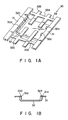
- Fig. 1A is a perspective view of a lead frame 30 used for fabricating a conventional hybrid resin-sealed semiconductor device.
- the lead frame 30 is obtained by pressing a conductive metallic plate.
- the specific construction of the lead frame 30 is as follows:
- a plurality of heat sinks 32 are provided between a pair of first frames 31 arranged in parallel to each other.
- a plurality of second frames 33a are also provided between the first frames 31 in such a manner that each second frame 33a is located between the adjacent heat sinks 32 and extends perpendicular to the first frames 31.
- internal leads 33b are arranged perpendicular to the second frames 33a. One end of each internal lead 33a is free, while the other end is located above the region in the neighborhood of the center of the heat sink 32.
- the second frames 33a and the internal leads 33b are integrally formed as one body.
- the heat sinks 32 are located slightly lower than the first frames 31.
- a pair of projections 32a are formed on each side of the heat sink 32, and a pair of through-holes 31a are formed in each of the first frames 31. After fitting the projections 32a in the respective through-holes 31a, those portions of the projections 32a extending out of the through-holes 31a are crushed flat, thereby fixing the heat sink 31 and the first frames 31 together.
- a pair of power ICs that is, semiconductor chips 36 of the same type are mounted on the heat sink 32 in an ordinary manner (only one of the power ICs being shown in Fig. 2).
- the pair of semiconductor chips 36 are secured to the heat sink 32 by use of an adhesive layer 37.
- the lead frame 30 is subjected to bonding step.
- An active or passive region is formed in the power ICs 36 by doping the impurities.
- at least one of electrodes, wiring layers, and pads electrically connected to the active or passive region is connected to the internal lead 34 by means of a thin metallic wire 29.
- the electrodes, wiring layers, or pads are normally connected to external elements.
- the bonding step ordinary ball bonding or ultrasonic ball bonding is utilized. As is shown in Figs. 2 and 3, the bonding first performed with respect to the thin metallic wire is ball bonding, and the bonding performed next is wedge bonding. The bonding with respect to the thin metallic wire is completed by performing these two kinds of bonding.
- a grounded point must be used in common to a plurality of power ICs, and the circuit components must be connected together in a predetermined fashion.
- a plurality of insulating substrates 38 formed of glass epoxy resin, are formed on the mounting positions on the heat sink 32.
- the insulating substrate 38 is secured to the heat sink 32 by use of the insulating adhesive material 28.
- the thin metallic wires 29 are used as jumpers.
- conductive coatings 40 are formed on the tops of insulating substrates 38 by deposition, and insulating layers 41 are provided for the prevention of a short circuit.
- insulating substrates 38 formed of glass epoxy resin
- interlayer insulating film 42 is formed on about a half of the surface of each conductive coating 40 which is formed on insulating substrate 38.
- a second conductive layer 43 may be formed on the interlayer insulating film 42, for the connection between electrodes of the power ICs 36 if it is necessary.
- the distance between the insulating substrate 38 and the power IC 36 must be at least 0.2 mm. In the case where two insulating substrates 38 are formed, they are spaced from each other by at least 0.5 mm, and thin metallic wires 29 formed of Al, Au or Cu and having a diameter in the range between 25 ⁇ m and 50 ⁇ m are employed.
- An insulating protection film 44 (not shown) is formed on both the conductive coatings 40 and the second conductive layer 43, so as to prevent coatings 40 and layer 43 from undesirably short-circuiting to other thin metallic wires 29.
- a normal resin sealing step is performed by use of the transfer mold process. Thereafter, the lead frame 30 is subjected to a cut and bend step to thus complete a semiconductor device.
- measure (1) results in a high manufacturing cost since conductive layers have to be formed as a laminated structure.
- Measure (2) also results in a high manufacturing cost, due to an increase in the number of steps required. More specifically, if jumpers 29 are arranged over two conductive coatings 40, as is shown in Fig. 2, the wires have to be coated with an insulating protection material, so as to prevent a short circuit between the jumpers 29 and the conductive coatings 40 at the time of the resin sealing step.
- the present invention has been developed in consideration of the above circumstances, and is intended to provide a hybrid resin-sealed semiconductor device which is simple in structure and requires neither a conductive multi layer formed within an insulating layer nor an insulating protection layer coated on the wires, and which enables intersection of wires without causing any short circuit.
- the hybrid resin-sealed semiconductor device comprises: a heat sink on which a plurality of semiconductor chips are mounted; an insulating substrate secured to the heat sink; conductive metallic layers formed on the insulating substrate; electrodes formed on the semiconductor chips; first thin metallic wires for connecting the electrodes and the conductive metallic layers together; conductive intermediate members integrally formed with the heat sink and located higher than the heat sink; second thin metallic wires for connecting the conductive intermediate member to points to which the first thin metallic wires are connected; and a molding member for sealing and securing the above-mentioned elements.
- the heat sink which is part of a casing and internal leads are different in level.
- the internal lead is used as a member for intermediating thin metallic wires in the bonding step.
- a hybrid integrated circuit device employing a power IC 2 is incorporated in a lead frame which comprises a heat sink 1, as in the prior art. After subjected to resin-sealing step, cut and bend step, etc., the hybrid integrated circuit device is completed.
- the lead frame provided with the heat sink used in the present invention is similar to that explained above with reference to Figs. 1 to 3.
- the present invention differs from the prior art, in that a lead frame located at different level from that of the heat sink is utilized as an intermediating member for intermediating thin metallic wires.
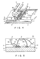
- Fig. 4 is a perspective view of the hybrid resin-sealed integrated circuit device according to the present invention.
- the integrated circuit device shown in Fig. 4 is in an unmolded state and includes a plurality of power ICs 2 which are mounted on the heat sink 1 in an ordinary manner.
- the heat sink 1 used in the present invention is of a depressed type, such that shown in Figs. 1A and 1B.
- the lead frame is obtained by pressing a conductive metallic plate, and comprises: a pair of first frames arranged in parallel to each other; a plurality of heat sinks 1 which are provided between the first frames so as to connect them and on which semiconductor devices are mounted; a plurality of second frames provided between the first frames in such a manner that each second frame is located between the adjacent heat sinks 1 so as to connect the first frames; and internal leads 3 arranged such that one end is fixed to the second frame and the other end is a free end located above the substantial center of the heat sink.
- the internal lead 3 is located higher than the heat sink 1. As is shown in Fig.
- a plurality of silicon power ICs 2 are secured on the heat sink 1 in an ordinary fashion by use of either a conductive adhesive or an Au-Si eutectic material.
- An insulating substrate 4 formed of glass epoxy resin is arranged such that it surrounds the power ICs 2.
- a conductive metallic layer 5 is formed on the insulating substrate 4 by patterning, such that the conductive metallic layer surrounds one of the power ICs 2.
- Fig. 5 is a sectional view taken along line A-A in Fig. 4 and illustrating a hybrid resin-sealed semiconductor device obtained after molding.
- the silicon power ICs 2 are mounted on, and secured to the heat sink 1 by use of the conductive adhesive layer 9 including the solder.
- the insulating substrate 4 is located between the silicon power ICs 2 and secured to the heat sink 1 by use of the insulating adhesive material 10.
- the conductive metallic layer 6 is formed on the top of the insulating substrate 4.
- the distance between the silicon power IC 2 and the insulating substrate 4 is not less than 0.2 mm, and the distance between the insulating substrates 4 is not less than 0.5 mm.
- an electrode 6 of one silicon power IC 2 is connected to the conductive metallic layer 6 by providing a first thin metallic wire 81, while the internal lead 3 i.e., the intermediating member 3 is connected to electrodes 6 of the other power ICs 2 and the conductive metallic layer 7 by providing second thin metallic wires 82.
- the first and second thin metallic wires are formed of Au, Al, Cu or another conductive metal, and has a diameter in the range between 25 ⁇ m and 50 ⁇ m.
- the bonding first performed with respect to the thin metallic wires 81 and 82 is either ultrasonic or ordinary ball bonding, and bonding performed next is wedge bonding. This bonding step is carried out by use of an ordinary bonding device.
- the bonding arm of the bonding device After performing the first bonding i.e., the ball bonding, the bonding arm of the bonding device is lifted and moved until it comes to a location where the second bonding should be performed. Therefore, the thin metallic wires 81 and 82 are extended between two different levels corresponding to the locus for which the bonding arm is moved, and therefore they form substantially triangular loops.
- the thin metallic wires 82 are extended between different levels, and therefore do not touch the electrodes 6 and 7 and conductive metallic layer if the wires 82 intersect the electrodes 6 and 7 and the layer 5. Even if the thin metallic wires 82 is pushed down in the resin-sealing step, it is not likely that the thin metallic wires 82 will touch the electrodes 6, 7 and the conductive metallic layer 5.
- a pair of power ICs 2 of the same type are mounted on the heat sink 1. Needless to say, however, three or more power devices of different types may be mounted on the heat sink.
- thermosetting resin 50 such as epoxy resin
- jumpers are arranged in such a manner that they do not short-circuit to one another.
- the semiconductor device can be manufactured without requiring a large number of steps. Therefore, the semiconductor device can be manufactured at a low cost.
- the portions to which the thin metallic wires are connected are located at different levels, the thin metallic wires are hard to short-circuit to one another even if they are exerted with external mechanical force. If the thin metallic wires are exerted with an extremely large external force, they will be broken, so that the semiconductor device will be detected as being defective.
Landscapes
- Structures Or Materials For Encapsulating Or Coating Semiconductor Devices Or Solid State Devices (AREA)
- Lead Frames For Integrated Circuits (AREA)
- Wire Bonding (AREA)
- Cooling Or The Like Of Semiconductors Or Solid State Devices (AREA)
Applications Claiming Priority (2)
| Application Number | Priority Date | Filing Date | Title |
|---|---|---|---|
| JP4051/89 | 1989-01-11 | ||
| JP894051A JPH02184054A (ja) | 1989-01-11 | 1989-01-11 | ハイブリッド型樹脂封止半導体装置 |
Publications (3)
| Publication Number | Publication Date |
|---|---|
| EP0378209A2 true EP0378209A2 (fr) | 1990-07-18 |
| EP0378209A3 EP0378209A3 (fr) | 1991-04-10 |
| EP0378209B1 EP0378209B1 (fr) | 1993-11-18 |
Family
ID=11574103
Family Applications (1)
| Application Number | Title | Priority Date | Filing Date |
|---|---|---|---|
| EP90100516A Expired - Lifetime EP0378209B1 (fr) | 1989-01-11 | 1990-01-11 | Dispositif semi-conducteur hybride encapsulé en résine |
Country Status (5)
| Country | Link |
|---|---|
| US (1) | US4984065A (fr) |
| EP (1) | EP0378209B1 (fr) |
| JP (1) | JPH02184054A (fr) |
| KR (1) | KR930004244B1 (fr) |
| DE (1) | DE69004581T2 (fr) |
Cited By (2)
| Publication number | Priority date | Publication date | Assignee | Title |
|---|---|---|---|---|
| EP0528291A3 (en) * | 1991-08-08 | 1994-05-11 | Sumitomo Electric Industries | Semiconductor chip module and method for manufacturing the same |
| SG109435A1 (en) * | 2000-12-07 | 2005-03-30 | Chuen Khiang Wang | Leaded mcm package and method therefor |
Families Citing this family (16)
| Publication number | Priority date | Publication date | Assignee | Title |
|---|---|---|---|---|
| JPH02201948A (ja) * | 1989-01-30 | 1990-08-10 | Toshiba Corp | 半導体装置パッケージ |
| JPH0724270B2 (ja) * | 1989-12-14 | 1995-03-15 | 株式会社東芝 | 半導体装置及びその製造方法 |
| JP2528991B2 (ja) * | 1990-02-28 | 1996-08-28 | 株式会社日立製作所 | 樹脂封止型半導体装置及びリ―ドフレ―ム |
| US5049973A (en) * | 1990-06-26 | 1991-09-17 | Harris Semiconductor Patents, Inc. | Heat sink and multi mount pad lead frame package and method for electrically isolating semiconductor die(s) |
| JP3074736B2 (ja) * | 1990-12-28 | 2000-08-07 | 富士電機株式会社 | 半導体装置 |
| JP2960283B2 (ja) * | 1993-06-14 | 1999-10-06 | 株式会社東芝 | 樹脂封止型半導体装置の製造方法と、この製造方法に用いられる複数の半導体素子を載置するためのリードフレームと、この製造方法によって製造される樹脂封止型半導体装置 |
| JP2938344B2 (ja) * | 1994-05-15 | 1999-08-23 | 株式会社東芝 | 半導体装置 |
| US5633785A (en) * | 1994-12-30 | 1997-05-27 | University Of Southern California | Integrated circuit component package with integral passive component |
| US5886414A (en) * | 1996-09-20 | 1999-03-23 | Integrated Device Technology, Inc. | Removal of extended bond pads using intermetallics |
| EP0903780A3 (fr) * | 1997-09-19 | 1999-08-25 | Texas Instruments Incorporated | Procédé et appareillage pour empaquetage à fils soudés pour circuits intégrés |
| US6169331B1 (en) | 1998-08-28 | 2001-01-02 | Micron Technology, Inc. | Apparatus for electrically coupling bond pads of a microelectronic device |
| SG109436A1 (en) * | 2000-12-07 | 2005-03-30 | Fung Leng Chen | Leaded mcm package and method therefor |
| JP5132070B2 (ja) * | 2006-03-31 | 2013-01-30 | オンセミコンダクター・トレーディング・リミテッド | 回路装置およびその製造方法 |
| JP5062283B2 (ja) * | 2009-04-30 | 2012-10-31 | 日亜化学工業株式会社 | 半導体装置及びその製造方法 |
| US20110042793A1 (en) * | 2009-08-21 | 2011-02-24 | Freescale Semiconductor, Inc | Lead frame assembly for a semiconductor package |
| US20120286409A1 (en) * | 2011-05-10 | 2012-11-15 | Jitesh Shah | Utilizing a jumper chip in packages with long bonding wires |
Family Cites Families (6)
| Publication number | Priority date | Publication date | Assignee | Title |
|---|---|---|---|---|
| US3784884A (en) * | 1972-11-03 | 1974-01-08 | Motorola Inc | Low parasitic microwave package |
| US4200880A (en) * | 1978-03-28 | 1980-04-29 | Microwave Semiconductor Corp. | Microwave transistor with distributed output shunt tuning |
| JPS58213456A (ja) * | 1982-06-04 | 1983-12-12 | Nec Corp | 半導体装置 |
| NL8202470A (nl) * | 1982-06-18 | 1984-01-16 | Philips Nv | Hoogfrequentschakelinrichting en halfgeleiderinrichting voor toepassing in een dergelijke inrichting. |
| JPS63141328A (ja) * | 1986-12-03 | 1988-06-13 | Mitsubishi Electric Corp | 高周波高出力トランジスタ |
| JPS63250164A (ja) * | 1987-04-07 | 1988-10-18 | Denki Kagaku Kogyo Kk | ハイパワ−用混成集積回路基板とその集積回路 |
-
1989
- 1989-01-11 JP JP894051A patent/JPH02184054A/ja active Pending
- 1989-12-29 US US07/459,318 patent/US4984065A/en not_active Expired - Lifetime
-
1990
- 1990-01-11 DE DE90100516T patent/DE69004581T2/de not_active Expired - Fee Related
- 1990-01-11 KR KR1019900000292A patent/KR930004244B1/ko not_active Expired - Fee Related
- 1990-01-11 EP EP90100516A patent/EP0378209B1/fr not_active Expired - Lifetime
Cited By (3)
| Publication number | Priority date | Publication date | Assignee | Title |
|---|---|---|---|---|
| EP0528291A3 (en) * | 1991-08-08 | 1994-05-11 | Sumitomo Electric Industries | Semiconductor chip module and method for manufacturing the same |
| US5525835A (en) * | 1991-08-08 | 1996-06-11 | Sumitomo Electric Industries, Ltd. | Semiconductor chip module having an electrically insulative thermally conductive thermal dissipator directly in contact with the semiconductor element |
| SG109435A1 (en) * | 2000-12-07 | 2005-03-30 | Chuen Khiang Wang | Leaded mcm package and method therefor |
Also Published As
| Publication number | Publication date |
|---|---|
| DE69004581D1 (de) | 1993-12-23 |
| KR930004244B1 (ko) | 1993-05-22 |
| JPH02184054A (ja) | 1990-07-18 |
| EP0378209B1 (fr) | 1993-11-18 |
| DE69004581T2 (de) | 1994-04-28 |
| EP0378209A3 (fr) | 1991-04-10 |
| US4984065A (en) | 1991-01-08 |
Similar Documents
| Publication | Publication Date | Title |
|---|---|---|
| EP0378209A2 (fr) | Dispositif semi-conducteur hybride encapsulé en résine | |
| US6781240B2 (en) | Semiconductor package with semiconductor chips stacked therein and method of making the package | |
| US5521429A (en) | Surface-mount flat package semiconductor device | |
| KR100342589B1 (ko) | 반도체 전력 모듈 및 그 제조 방법 | |
| EP0498446B1 (fr) | Dispositif encapsulé à plusieurs puces semi-conductrices et procédé pour sa fabrication | |
| EP0247775B1 (fr) | Empaquetage pour semi-conducteurs ayant des connexions entrée/sortie à haute densité | |
| US5708304A (en) | Semiconductor device | |
| JPH05109972A (ja) | リードフレーム及び集積回路チツプのパツケージ・アセンブリ | |
| KR100203934B1 (ko) | 패턴닝된 리드프레임을 이용한 멀티 칩 패키지 | |
| KR19990013634A (ko) | 반도체 패키지 본드 포스트의 배치 및 설계 방법 | |
| US8445998B1 (en) | Leadframe structures for semiconductor packages | |
| US7247944B2 (en) | Connector assembly | |
| US7274092B2 (en) | Semiconductor component and method of assembling the same | |
| US5349233A (en) | Lead frame and semiconductor module using the same having first and second islands and three distinct pluralities of leads and semiconductor module using the lead frame | |
| EP0253295A1 (fr) | Boîtier à diffusion thermique améliorée pour circuit intégré LSI | |
| US5559305A (en) | Semiconductor package having adjacently arranged semiconductor chips | |
| US5393705A (en) | Molded semiconductor device using intermediate lead pattern on film carrier formed from lattice pattern commonly available for devices and process of fabrication thereof | |
| USRE36894E (en) | Semiconductor package with high density I/O lead connection | |
| KR100891649B1 (ko) | 반도체 패키지 제조방법 | |
| JPS63255953A (ja) | 絶縁物封止型回路装置 | |
| US20250385193A1 (en) | A leadless package comprising a first and a second semiconductor die, wherein a galvanic coupling is provided between those semiconductor dies, as well as a corresponding method | |
| US5434450A (en) | PGA package type semiconductor device having leads to be supplied with power source potential | |
| JP3127948B2 (ja) | 半導体パッケージ及びその実装方法 | |
| KR0120186B1 (ko) | 버퍼칩을 이용한 반도체 장치 및 그 제조방법 | |
| KR20020021476A (ko) | 칩 스케일 반도체 팩키지 및, 그것의 제조 방법 |
Legal Events
| Date | Code | Title | Description |
|---|---|---|---|
| PUAI | Public reference made under article 153(3) epc to a published international application that has entered the european phase |
Free format text: ORIGINAL CODE: 0009012 |
|
| 17P | Request for examination filed |
Effective date: 19900111 |
|
| AK | Designated contracting states |
Kind code of ref document: A2 Designated state(s): DE FR GB |
|
| PUAL | Search report despatched |
Free format text: ORIGINAL CODE: 0009013 |
|
| AK | Designated contracting states |
Kind code of ref document: A3 Designated state(s): DE FR GB |
|
| 17Q | First examination report despatched |
Effective date: 19920515 |
|
| GRAA | (expected) grant |
Free format text: ORIGINAL CODE: 0009210 |
|
| AK | Designated contracting states |
Kind code of ref document: B1 Designated state(s): DE FR GB |
|
| REF | Corresponds to: |
Ref document number: 69004581 Country of ref document: DE Date of ref document: 19931223 |
|
| ET | Fr: translation filed | ||
| PLBE | No opposition filed within time limit |
Free format text: ORIGINAL CODE: 0009261 |
|
| STAA | Information on the status of an ep patent application or granted ep patent |
Free format text: STATUS: NO OPPOSITION FILED WITHIN TIME LIMIT |
|
| 26N | No opposition filed | ||
| PGFP | Annual fee paid to national office [announced via postgrant information from national office to epo] |
Ref country code: FR Payment date: 19980109 Year of fee payment: 9 |
|
| PGFP | Annual fee paid to national office [announced via postgrant information from national office to epo] |
Ref country code: DE Payment date: 19980116 Year of fee payment: 9 |
|
| REG | Reference to a national code |
Ref country code: GB Ref legal event code: 746 Effective date: 19981002 |
|
| PG25 | Lapsed in a contracting state [announced via postgrant information from national office to epo] |
Ref country code: FR Free format text: LAPSE BECAUSE OF NON-PAYMENT OF DUE FEES Effective date: 19990930 |
|
| PG25 | Lapsed in a contracting state [announced via postgrant information from national office to epo] |
Ref country code: DE Free format text: LAPSE BECAUSE OF NON-PAYMENT OF DUE FEES Effective date: 19991103 |
|
| REG | Reference to a national code |
Ref country code: FR Ref legal event code: ST |
|
| REG | Reference to a national code |
Ref country code: GB Ref legal event code: IF02 |
|
| PGFP | Annual fee paid to national office [announced via postgrant information from national office to epo] |
Ref country code: GB Payment date: 20070110 Year of fee payment: 18 |
|
| GBPC | Gb: european patent ceased through non-payment of renewal fee |
Effective date: 20080111 |
|
| PG25 | Lapsed in a contracting state [announced via postgrant information from national office to epo] |
Ref country code: GB Free format text: LAPSE BECAUSE OF NON-PAYMENT OF DUE FEES Effective date: 20080111 |