EP0378440A2 - Bilderzeugungsgerät - Google Patents
Bilderzeugungsgerät Download PDFInfo
- Publication number
- EP0378440A2 EP0378440A2 EP90300382A EP90300382A EP0378440A2 EP 0378440 A2 EP0378440 A2 EP 0378440A2 EP 90300382 A EP90300382 A EP 90300382A EP 90300382 A EP90300382 A EP 90300382A EP 0378440 A2 EP0378440 A2 EP 0378440A2
- Authority
- EP
- European Patent Office
- Prior art keywords
- image
- developing
- bearing member
- potential
- peak
- Prior art date
- Legal status (The legal status is an assumption and is not a legal conclusion. Google has not performed a legal analysis and makes no representation as to the accuracy of the status listed.)
- Ceased
Links
Images


Classifications
-
- G—PHYSICS
- G03—PHOTOGRAPHY; CINEMATOGRAPHY; ANALOGOUS TECHNIQUES USING WAVES OTHER THAN OPTICAL WAVES; ELECTROGRAPHY; HOLOGRAPHY
- G03G—ELECTROGRAPHY; ELECTROPHOTOGRAPHY; MAGNETOGRAPHY
- G03G15/00—Apparatus for electrographic processes using a charge pattern
- G03G15/01—Apparatus for electrographic processes using a charge pattern for producing multicoloured copies
- G03G15/0105—Details of unit
- G03G15/0121—Details of unit for developing
-
- G—PHYSICS
- G03—PHOTOGRAPHY; CINEMATOGRAPHY; ANALOGOUS TECHNIQUES USING WAVES OTHER THAN OPTICAL WAVES; ELECTROGRAPHY; HOLOGRAPHY
- G03G—ELECTROGRAPHY; ELECTROPHOTOGRAPHY; MAGNETOGRAPHY
- G03G15/00—Apparatus for electrographic processes using a charge pattern
- G03G15/06—Apparatus for electrographic processes using a charge pattern for developing
- G03G15/08—Apparatus for electrographic processes using a charge pattern for developing using a solid developer, e.g. powder developer
- G03G15/09—Apparatus for electrographic processes using a charge pattern for developing using a solid developer, e.g. powder developer using magnetic brush
- G03G15/0907—Apparatus for electrographic processes using a charge pattern for developing using a solid developer, e.g. powder developer using magnetic brush with bias voltage
Definitions
- the present invention relates generally to an image forming apparatus, more particularly to a color image forming apparatus such as an electrophotographic copying machine, a printer or a compound recording apparatus wherein a visible image in plural colors can be formed through a one printing cycle.
- a color image forming apparatus such as an electrophotographic copying machine, a printer or a compound recording apparatus wherein a visible image in plural colors can be formed through a one printing cycle.
- a plurality of developing devices are disposed adjacent to an outer periphery of an image bearing member, that is, a photosensitive drum to transfer at once the plural color images onto a transfer material.
- an image bearing member that is, a photosensitive drum
- various proposals have been made as to methods for preventing the visualized image provided by an upstream developing device from being disturbed by being rubbed with the developer of the downstream developing device, with respect to the rotational directions of the photosensitive drum.
- U.S. Patents Nos. 457265 and 4,416,533 propose that developing bias voltages having only DC components are applied to the two developing devices to develop the images with the developers contained in the developing devices.
- Japanese Laid-Open Patent Application No. 12650/1981 proposes that a developing bias voltage having only a DC component is applied to the downstream developing device, and the visualized image is formed without contact of the developer to the outer surface of the photosensitive drum.
- Japanese Laid-Open Patent Application No. 144452/1981 and U.S. Patent No. 4,349,268 propose that a developing bias voltage is applied to the downstream developing device, and the visualized image is formed without contact of the developer to the outer surface of the photosensitive drum.
- U.S. Patent No. 4,660,961 proposes that before the electrostatic latent image to be developed by the downstream developing device is formed, a potential level of the image visualized by the upstream developing device is increased.
- Japanese Laid-Open Patent Application No. 210861/1988 U.S. Serial No. 161,029
- Japanese Laid-Open Patent Application No. 219773/1989 propose an image forming apparatus wherein a developing bias voltage having an AC component is applied to the downstream developing device, and wherein the above problems are solved.
- a developing bias voltage having an AC component is applied to the downstream developing device, and wherein the above problems are solved.
- Figure 1 shows a relation between the AC voltage component and the DC voltage component of the developing bias applied to the downstream developing device, wherein the ordinate represents a DC voltage component (Vdc), and the abscissa represents a peak-to-peak voltage (Vpp) of the AC component.
- Vdc DC voltage component
- Vpp peak-to-peak voltage
- a line A represents the requirement for preventing production of foggy background
- a chain line B represents a requirement for preventing toner mixture.
- Those lines were determined on the basis of experimental data (frequency of the developing bias was 1600 Hz, the potential of the latent image was the same as in the embodiment which will be described hereinafter, and the distance d between the developing sleeve and the photosensitive member was 300 microns).
- the region below the line A and above the line B is an optimum area wherein the two requirements are satisfied.
- the peak-to-peak voltage Vpp is required to be not more than 850, as shown in Figure 1.
- the image density here, was measured from a solid image of 5 mm square using a reflection density measuring device available from McBeth under the name of RD 514, for example.
- the line width here, was measured from two dot line printed with five dot space in 300 DPI, using a line width measuring device, available from Konishiroku Shashin Kogyo Kabushiki Kaisha, Japan, under the name of FBD line density measuring device.
- the AC voltage has a duty ratio of 1:1, and the DC voltage component is adjusted, as disclosed in the Japanese Laid-Open Application, the adjustable range is narrow, and in addition, when the voltage of the voltage source varies, the image quality is easily deteriorated, and the developer is easily mixed into the downstream developing device.
- a main assembly of the image forming apparatus includes an image bearing member, that is, an electrophotographic photosensitive drum 1 disposed adjacent the center of the main assembly.
- the photosensitive drum 1 is rotatable in a direction indicated by an arrow A.
- An image exposure means includes a polygonal mirror 14, a polygonal mirror driving motor 34, a semiconductor laser 12, another semiconductor laser 13, an image lens 16 and a reflection mirror 17.
- the second developing device 7 has a developer carrying member in the form of a rotational sleeve 7a in this embodiment, to which a developing bias voltage source 15 is connected.
- the first developing device 4 also has a rotational sleeve 4a to which a known developing bias voltage source (not shown) is connected.
- a cleaning device 11 functions to remove the developer remaining on the outer periphery of the photosensitive drum 1.
- the primary charger 2 acts on the outer peripheral surface of the photosensitive drum 1 after it is cleaned by the cleaning device 11 to uniformly charge the photosensitive drum1 with a negative voltage of approximately -600 V.
- the semiconductor laser 12 produces a first laser beam 3 modulated in accordance with a first information signal produced by an unshown controller; and the semiconductor laser 13 produces a second laser beam 6 modulated in accordance with a second information signal produced by the controller; and the beams are separately projected on the photosensitive drum 1.
- the polygonal mirror 14 rotated by the motor 34 receives a first laser beam 13 emitted from the semiconductor laser 12 and deflects it to raster-scans the outer peripheral surface of the photosensitive drum 1 at a position indicated by a reference L1 through an imaging lens 16 and a reflection mirror 17.
- a first latent image is formed having a surface potential of approximately -100 V (light portion potential) at a portion exposed to the laser beam.
- the polygonal mirror 14 receives the second laser beam 6 emitted from the semiconductor laser 13 and raster-scans the photosensitive drum 1 at a position L2 through the imaging lens 16, the photosensitive drum 1 having a first visualized image provided by the first developing device 4 and having been uniformly charged to a predetermined potential of a negative polarity by the secondary charger 5.
- a second electrostatic latent image is formed having a surface potential of approximately -100 V (light portion potential V1) at a portion exposed to the laser beam.
- the developing sleeve 4a of the first developing device 4 carries to a developing position a two component developer including red toner negatively charged and magnetic carrier particles of ferrite or the like.
- a developing bias voltage which is a superposed DC voltage component and AC voltage component from a developing bias source (not shown) is applied, by which the first electrostatic latent image is reverse-developed with the red toner.
- the bias voltage applied to the sleeve 4a may consist only of the DC component.
- the secondary charger 5 is effective to uniformly charge again, to a predetermined potential of the negative polarity, the outer peripheral surface of the photosensitive drum on which the visualized image has been formed with the red developer by the first developing device 4.
- the developing sleeve 7a of the second developing device 7 carries to a developing position a one component developer (toner) of black color negatively charged.
- a vibratory voltage having alternating maximum level and minimum level from a voltage source which will be described hereinafter, is applied to form a vibratory electric field in the developing position where the developer is transferred from the sleeve 7a to the drum 1.
- the sleeve 7a carries a layer of the developer having a thickness smaller than the minimum clearance between the drum 1 and the sleeve 7a in the developing position, and the developer transfers to the drum 1 by the vibratory electric field.
- the developing device 7 reverse-develops the second latent image.
- the black toner of the developing device 7 is deposited on the light potential portion of the second latent image which has been exposed to the laser beam 6, by which the latent image is visualized.
- the second developing device 7 forms the black toner image on the surface of the drum which already have the red toner image provided by the first developing device 4.
- the two visualized images are transferred at once to a transfer material 9 by the transfer charger 8, and are fixed by an unshown image fixing device.
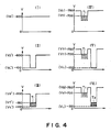
- Figure 4 shows the surface potential of the photosensitive member 1 in the electrophotographic process shown in Figure 2.
- the ordinate represents a negative potential (V)
- the abscissa represents a longitudinal (main scanning direction) position on the photosensitive member 1.
- the primary charger 2 charges the photosensitive member 1 to -600 V as shown in Figure 4(I).
- a first electrostatic latent image having a dark portion potential V′D of -600 V and a light portion potential V′L of -100 V.
- the first developing device 4 develops the first electrostatic latent image, so that a first toner image T1 is formed, as shown in Figure 4(III).
- the potential V′T of the first toner image is approximately -150 V.
- the secondary charger 5 charges the photosensitive member 1, by which the potential VT of the first toner image becomes approximately -700 V, as shown in Figure 4(IV).
- the second laser beam 6 is projected, so that as shown in Figure 4(V), a second electrostatic latent image is formed which has a dark portion potential VD of -750 V and a light portion potential VL of approximately -100 V.
- the second developing device 7 develops the second electrostatic latent image to form the second toner image T2, as shown in Figure 4(VI).
- the first and second toner images T1 and T2 are transferred onto the transfer sheet 9 by the transfer charger 8.
- the first toner image T1 receives two forces.
- One is the force which is provided by the electric field for moving the negatively charged toner away from the sleeve and toward the photosensitive member and which is proportional to
- the other is a force which is provided by an electric field for moving the toner away from the photosensitive member toward the sleeve and which is proportional to
- the two forces are applied.
- One is the force provided by the electric field for moving the negatively charged black toner away from the sleeve toward the photosensitive member and which is proportional to
- the other is the force which is provided by the electric field for moving the toner away from the photosensitive member toward the sleeve to remove the black toner from the photosensitive member and which is proportional to
- VA1 and VA2 are the minimum and maximum levels of the bias voltage E
- VT is a potential of the first toner image.
- V DC is a time average of the vibratory bias voltage E, that is, a time-integrated level of the vibratory bias voltage is one period (t A1 + t A2 ). In the specification, this is called an average or integration of the vibratory bias voltage.
- the minimum level VA1 of the developing bias voltage is effective to urge the developer to the electrostatic latent image formed on the outer peripheral surface of the photosensitive drum to visualize the latent image. More particularly, the voltage VA1 acts on the red developer forming the first visualized image on the photosensitive drum 1 to urge the red developer to the photosensitive drum 1 in proportion to
- the maximum level VA2 of the developing bias voltage acts on the developer visualizing the latent image on the photosensitive drum to move it away from the photosensitive drum. That is, the voltage VA2 applies force to the red developer of the first visualized image in the direction away from the photosensitive drum in proportion to
- the mixture of the red developer of the first visualized image into the second developing device 7 is dependent on the force proportional to
- /d ⁇ 2.25 [V/micron] (1) as disclosed in U.S. serial No. 161,029, from the standpoint of preventing the mixture. Then, when VT -700 V, and the clearance between the developing sleeve 7a and the photosensitive drum 1 is 300 microns (d), the voltage VA2 has to be not more than -25 V. On the contrary, if the voltage VA2 is too small, a foggy background is produced in the copy image. The above-described influence is dependent on the time during which the voltage VA2 is applied, which will be described in conjunction with V DC , in the following paragraph.
- the time average of the developing bias voltage (rectangular pulse signal E) has the influence similar to the DC component V DC of the developing bias voltage when the pulse duty ratio is 5:5.
- the black developer in the second developing device moves toward the photosensitive drum 1 surface.
- an amount of the black developer which is proportional to VA1 x t A1 is deposited on the outer surface of the photosensitive drum 1.
- the black developer forming the second visualized image moves away from the photosensitive drum 1 to the sleeve 7a of the second developing device 7.
- V DC is between VT and VL.
- VA1, VA2 and V DC have respective preferable ranges because of the image density, line width, sharpness, mixture in color, foggy background production or the like of the copy image.
- VD -750 V
- VL -100 V
- VT -700 V
- d 300 microns, -1500 V ⁇ VA1 ⁇ -900 V, VA2 ⁇ -25 V, -700 V ⁇ V DC - ⁇ 500 V.
- VA1, VA2 and V DC are preferably selected so as to satisfy the following:
- equation (1) improves the image density and reproducibility of a thin line; (2) improves prevention of the mixture of the first toner into the second developing device 7; and (3) improves the image density and the line width.
- the requirement (4) improves the image density and the reproducibility of a thin line; the requirement (5) improves the mixture of the first toner into the second developing device 7; and (6) improves the image density and the line width.
- Figure 6A shows the ranges of the voltages VA1 and VA2 which satisfy the various requirements relating to the image density, line width, sharpness, toner mixture and fog prevention of the copy image when the duty ratio of the developing bias voltage applied to the developing sleeve 7a is fixed to be 5:5.
- Figure 6B shows regions of VA1 and VA2 satisfying the various requirements when the duty ratio of the developing bias voltage applied to the developing sleeve 7a is changed. In Figures 6A and 6B, the regions are indicated as hatched areas.
- the changes in the surface potentials VD and VL or the like on the surface of the photosensitive drum 1 result from changes in the ambient conditions under which the image forming apparatus of this embodiment is placed or changes in the charging conditions for the photosensitive drum 1.
- duty ratio means a ratio between the time of one period in which a voltage higher than a middle of the vibratory voltage between the maximum level and the minimum level, that is, ((maximum voltage) + (minimum voltage))/2 continues and the time of one period in which a voltage smaller than that continues.
- the waveform is rectangular, and therefore, the duty ratio is t A1 :t A2 .
- the developing bias voltage source 15 includes an oscillator 18, a comparator 19 having a function of wave reformer (particularly a slicer), a comparator (differential amplifier) 28, an amplifier 20, a transformer 21, capacitors C1 and C2, resistors R1 and R2, a crumpling diode D1, a constant voltage source 27, an output terminal P1 and input terminal P2.
- the oscillator 18 produces a triangular pulse signal in the form shown in Figure 3 (I).
- the comparator 19 reads the triangular pulse signal produced by the oscillator 18, and also reads an error voltage level signal produced by the comparator 28.
- the comparator 19 compares the triangular pulse signal and the error voltage level signal, and produces a triangular pulse signal having an on-time period (that is, pulse duty ratio) corresponding to the result of the comparison.
- the comparator 19 produces a rectangular pulse signal P having the on-time width (pulse duty ratio) shown in Figure 3 (II).
- a rectangular pulse signal Q having the on-time width (pulse duty ratio) shown in Figure 3 (III) is produced.
- a rectangular pulse signal R having the on-time width (pulse duty ratio) shown in Figure 3 (IV) is produced.
- the amplifier 20 receives the rectangular pulse signal P (Q or R) produced by the comparator 19 and amplifies it.
- the transformer 21 receives the rectangular pulse signal P (Q or R) amplified by the amplifier 20 and increases the signal in the voltage.
- the capacitor C1 receives the output signal from the transformer 21 and cramps it.
- the resistors R1 and R2 constitute a voltage dividing circuit.
- the capacitor C1 functions as a smoothing capacitor.
- the voltage dividing circuit and the capacitor C2 receive the output voltage signal from the transformer 21 and smoothes it and divides it in the voltage, and then the voltage drop across the resistor R2 is supplied to the comparator 28.
- the comparator 28 compares the voltage drop across the resistor R2 and a reference voltage signal corresponding to the target integration applied from the reference voltage source 22 to the input terminal P2, and in response to the result of the comparison (the difference between the actually output the integration and the target integration), and the comparator 28 produces an error voltage level signal shown by references P′, Q′ and R′ in Figure 3 (I).
- the maximum level VA2 of the developing bias voltage produced from the output terminal T1 is maintained substantially constantly at -100 V, that is, the constant level determined by the constant voltage circuit 27.
- the integration V DC of the developing bias voltage is substantially maintained constant at a level determined by the reference voltage applied to the terminal P2.
- FIG. 7 shows an image forming apparatus according to another embodiment of the present invention.
- the image forming apparatus according to this embodiment includes, in addition to the elements of the image forming apparatus shown in Figure 2, a potential sensor 29 for detecting the drum surface temperature after it is charged by the second charger 5, and an A/D transducer 30, D/A transducer 32 and a microcomputer (CPU) 31.
- a signal level of the surface potential VT of the first toner image on the photosensitive drum 1, produced by the potential sensor 29 is converted to a digital signal by the A/D transducer 30.
- the CPU 31 calculates, in response to the digital signal, the voltage VA2 to make constant
- FIG 8 shows an image forming apparatus according to a further embodiment of the present invention.
- the image forming apparatus of this embodiment includes, in addition to the elements shown in Figure 7, a D/A converter 33.
- a signal level of the light portion potential VL of the second latent image formed on the photosensitive drum, produced by the potential sensor 29 is converted to a digital signal by the A/D converter 30.
- the CPU 31 calculates a level of the voltage V DC to make substantially constant
- a signal is supplied to the variable reference voltage source 23 to the D/A converter.
- Figure 9 shows a bias circuit.
- an operator can selectively apply a rectangular wave, for example, having different duty ratios Figure 7 (a) and (b) to the developing sleeve 7a, in the manner which will be described hereinafter. Then, the image density and the line width of the second toner can be adjusted so that the equation (1) is satisfied, and the foggy background of the second developed image can be prevented.
- the circuit of Figure 9 embodiment is provided with an image quality adjusting means 47 having a variable resistor VR1 for permitting the operator to manually select the image quality.
- the amplifier 28 compares the integration VDC of the vibrator voltage actually applied to the sleeve 7a and a voltage level signal (a signal corresponding to the target integration) corresponding to the variable image density produced by the image quality adjusting means 47 constituted by the resistors R3 and R4 and a variable resistor VR1, and it amplifies the difference therebetween and applies it to the comparator 19. By doing so, the integration of the vibration voltage applied to the sleeve 7a is substantially maintained at the target integration level.
- the integration level of the vibrating bias voltage can be manually changed by the image adjusting means 47, in response to which the duty ratio changes as shown in Figure 10 which will be explained in detail hereinafter. At this time, the minimum and maximum levels VA1 and VA2 of the vibrating bias voltage do not change.
- the maximum level VA2 is determined in response to the voltage VE of the voltage source 45.
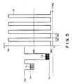
- Figure 10 shows the developing bias to explain the operation of the circuit of Figure 9, and the ordinate represents the bias voltage, and the abscissa represent time.
- VA2 represents the maximum level (-100 V) of the vibrating bias voltage E
- VA1 represents the minimum level (-1300 V) of the vibrating bias voltage E.
- the frequency of oscillation is 1600 Hz.
- the integration V DC is -600 V.
- the duty ratio t A1 :t A2 4.2:5.8.
- the image density and the line width can be adjusted within a sufficiently wide range without the toner mixture into the second developing device 7 and without the production of the foggy background.
- the minimum and maximum peak levels VA1 and VA2 of the vibratory bias voltage even if the integration V DC is changed more particularly, for example, the strength of the foggy background producing electric field (
- the developing bias is so controlled that the image portion potential VL of the second toner image, the image portion potential VT of the first toner image and the integration level V DC satisfy the above given equations (1) - (3), or (4) - (6).
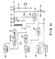
- Figure 11 is a block diagram of a developing bias source circuit of a multi-color image forming apparatus according to a further embodiment.
- the oscillation circuit 81 produces a rectangular wave (duty ratio is 1:1) having a frequency of 1500 Hz as shown in Figure 12(a) to a modulation circuit (comparator) 83
- the oscillation circuit 82 produces a rectangular wave (duty ratio is 1:1) having a frequency of 50 KHz shown in Figure 12(b) to a modulation circuit 84.
- the circuit further comprises a comparator (CMP) 83 which compares the output of an error amplifier 28 and the rectangular wave of 1500 Hz produced by the oscillation circuit (OSC) 81, and it supplies the difference therebetween to the modulation circuit 84.
- a switching circuit (SWC) 85 is closed when the output of the comparator 83 is at H-level, and at this time, a converter transformer 21 and the amplifier 28 are isolated.
- a microcomputer (CPU) 86 sets a required integration level V DC of the vibratory bias voltage to the error amplifier 28 through a D/A converter 87.
- the circuit includes a capacitor C3 and diodes D2 and D3.
- Figure 12 shows a voltage waveform for illustrating the operation of various parts of Figure 11.
- Figure 12(a) shows the rectangular waveform of 1500 Hz produced by the oscillation circuit 82;
- Figure 12(b) shows a rectangular wave of 50 KHz produced by the oscillation circuit 81;
- Figure 12(c) shows an output 83a of the comparator 83;
- Figure 12(d) shows an output 84a of the modulation circuit 84;
- Figure 12(e) shows an output 85a of the switching circuit 85;
- Figure 12(f) shows an output (a vibratory bias voltage E) at the outlet port P1.
- the converter transformer 44 is of a high frequency drive type, and therefore, the size thereof can be reduced.
- the modulation circuit 84 modulates the rectangular wave in accordance with the output 83a from the comparator 83.
- the switching circuit 85 is closed when the output 83a of the comparator 83 is at H-level, so that the converter transformer 21 and the amplifier 20 are isolated. Therefore, a voltage V1 is provided at the cathode side of the diode D3 while the switching circuit 85 is operated at the frequency of 50 KHz, and it is smoothed by the cramping capacitor C3 and the load capacity. Therefore, the output 85a of the switching circuit 85 is as shown in Figure 12(e). The produced output 85a is supplied to the output port P1 by the cramping capacitor C1. The diode D1 is rendered conductive at the forward peak.
- the output 85a of the switching circuit 85 is smoothed and divided in the voltage by a predetermined ratio by a smoothing circuit constituted by the resistors R1 and R2 and a capacitor C2. Thereafter an average level thereof is supplied to the error amplifier 28.
- the error amplifier 28 is responsive to the voltage level and the digital data produced by the CPU 86 to amplify a difference from an integration V DC of the vibrator bias voltage produced by the D/A converter 87, and the resultant signal level (P′, Q′, R′ or the like).
- the comparator 83 compares the output of the oscillator 81 and the output of the error amplifier 28, and produces a pulse-width-modulated output (PWM), for example the control signal A (output 83a) shown in Figure 12(c).
- PWM pulse-width-modulated output
- the switching circuit 85 is driven, and the signal is supplied to the modulation circuit 84, by which the output of the oscillation circuit 82 is modulated as shown in Figure 12(d). It is, then, supplied to the converter transformer 21 through the amplifier 20. In this manner, the vibratory voltage E ( Figure 12(f)) applied to the sleeve 7a of the second developing device, is provided.
- the vibratory bias voltage (developing bias) E is not completely rectangular particularly at the rising portion of the pulse.
- the integration V DC of the developing bias E is controlled to be constant, the same quality images can be provided with the same developing bias conditions irrespective of the waveform, by employing a system wherein the duty ratio is changed.
- the image can be stabilized at all times because the integration V DC of the developing bias E most relevant to the image quality is controlled to be substantially constant.
- the image quality can be sufficiently stabilized and assured even if the waveform of the developing bias E changes due to variation in the load of the second developing device 7, or the variation in the developing bias waveform due to the variation in the individual developing bias voltage sources.
- the integration level of the developing bias E since the integration level of the developing bias E is changed through the CPU 86, the integration level of the developing bias E can be changed in response to the steps of the control sequence such as the pre-rotation before the image formation on the drum or a post rotation after the image formation or the interval between an image formation and a subsequent image formation in an electrophotographic copying apparatus.
- Figure 13 is a timing chart illustrating the developing bias control in accordance with an electrophotographic process.
- reference LON indicates a laser beam emitting signal
- I indicates the pre-rotation period before the start of the image formation
- II and IV indicate printing periods (image formation period)
- III indicates an interval between one printing period and a subsequent printing period
- V designates a post-rotation period after the completion of the image formation.
- the laser beam emitting signal LON becomes high so as to permit the control of the quantity of light of the laser beam for forming the second image.
- the integration level V DC of the developing bias E applied to the second developing device 7 is maintained at high as possible level (-200 V in this embodiment).
- the integration level V DC of the developing bias E is changed to -500 V so that an optimum multi-color image can be provided.
- the integration level of the developing bias E increased to -200 V for the same reason as in the period I (light amount control).
- the light amount control is not effected, so that the integration level of the developing bias E is maintained at -500 V.
- the first color toner is prevented from mixing into the second developing device 7, and in addition, in the next image formation, a multi-color print is possible with sufficient sharpness, image density and reproducibility.
- the operator can manually set the target integration level by the CPU 86 in accordance with the image quality desired by the operator.
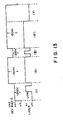
- Figure 14 is a block diagram illustrating the developing bias circuit for a multi-color image forming apparatus of this embodiment.
- the same reference numerals as in Figure 2 are assigned to the elements having the corresponding functions.
- the circuit includes a variable resistor 91 to control a gain of the amplifier 20 to adjust the minimum level VA1 of the bias voltage E.
- the variable resistor 91 is operated manually by an operator in association with the image adjusting means 47. It controls the amplitude of the input signal to the converter transformer 21 to change the minimum level VA1.
- Figure 15 shows the developing bias voltage produced by the circuit of Figure 14.
- Figure 15(a) shows a vibrating bias voltage E1 which is provided when the minimum level is -1500 V, the maximum level VA2 is -100 V, the frequency is 1500 Hz, the duty ratio t A1 :t A2 is 2.9:7.1, and the integration V DC is -500 V.
- Figure 15(b) shows a vibratory bias voltage E2, which is provided when the minimum level VA1 is -1000 V, the maximum level VA2 is -100 V, the frequency is 1500 Hz, the duty ratio t A1 :t A2 is 1.7:8.3, and the integration V DC is -250 V.
- the duty ratio is 1.1:8.9 to provide the integration level V DC of -250 V under the condition that the minimum level VA1 of the bias voltage E is -1500 V. Then, the steep rising is required to the developing bias waveform. If the rising becomes dull due to load variation or the like of the developing bias E, the control becomes not possible with the result that it is difficult to provide wide variable range of the integration level, so that the minimum level VA1 of the bias voltage E can not be reduced. Thus, it becomes difficult that the difference from the image portion potential VL is made large.
- variable resistor VR1 When the variable resistor VR1 is changed to change the integration level, the gain of the amplifier 20 is changed in accordance with the variable resistor 91 change, by which the integration level can be sufficiently made larger, while the minimum level VA1 of the bias voltage E can be reduced. Therefore, an image having good reproducibility of the thin line can be provided, and in addition the variable range of the line width can be made wider.
- the maximum level VA2 of the vibratory bias voltage E is fixed by the voltage source 45, and therefore, the toner of the first color is prevented from mixing into the second developing device 7.
- the laser beam is modulated in accordance with a signal indicative of the image to be recorded.
- the light image to which the photosensitive member is exposed can be provided by an array of light emitting diodes, an array of liquid crystal shutter or the like driven in accordance with information signal.
- the waveform of the developing bias is rectangular. However, it is not limiting, and a triangular wave or sine wave form are usable.
- the waveform may be any if pulse width modulation (PWM) is possible.
- the usable developers are not limited, and may be a two component developer, one component magnetic developer and one component non-magnetic developer.
- the toner is negatively charged, but, the present invention is applicable to an image forming apparatus using a positively charged toner.
- the voltage level VA1 and the voltage level VA2 are interchanged, in the foregoing descriptions.
Landscapes
- Physics & Mathematics (AREA)
- General Physics & Mathematics (AREA)
- Developing For Electrophotography (AREA)
- Color Electrophotography (AREA)
- Dry Development In Electrophotography (AREA)
Applications Claiming Priority (4)
| Application Number | Priority Date | Filing Date | Title |
|---|---|---|---|
| JP4760/89 | 1989-01-13 | ||
| JP476089 | 1989-01-13 | ||
| JP115532/89 | 1989-05-09 | ||
| JP11553289 | 1989-05-09 |
Publications (2)
| Publication Number | Publication Date |
|---|---|
| EP0378440A2 true EP0378440A2 (de) | 1990-07-18 |
| EP0378440A3 EP0378440A3 (de) | 1990-10-03 |
Family
ID=26338592
Family Applications (1)
| Application Number | Title | Priority Date | Filing Date |
|---|---|---|---|
| EP19900300382 Ceased EP0378440A3 (de) | 1989-01-13 | 1990-01-12 | Bilderzeugungsgerät |
Country Status (2)
| Country | Link |
|---|---|
| US (1) | US5066979A (de) |
| EP (1) | EP0378440A3 (de) |
Cited By (2)
| Publication number | Priority date | Publication date | Assignee | Title |
|---|---|---|---|---|
| EP0429309A3 (en) * | 1989-11-22 | 1991-11-06 | Xerox Corporation | Biasing scheme for improving latitudes in the tri-level xerographic process |
| EP0990957A3 (de) * | 1998-09-28 | 2001-03-14 | Canon Kabushiki Kaisha | Verfahren zum Einstellen der Entwicklungsdichte in einem Bilderzeugungsgerät |
Families Citing this family (26)
| Publication number | Priority date | Publication date | Assignee | Title |
|---|---|---|---|---|
| US5677099A (en) * | 1990-04-19 | 1997-10-14 | Canon Kabushiki Kaisha | Method of developing electrostatic latent image using oscillating bias voltage |
| US5187523A (en) * | 1990-09-12 | 1993-02-16 | Canon Kabushiki Kaisha | Developing apparatus for developing electrostatic latent image using two component developer |
| JP2938543B2 (ja) * | 1990-10-05 | 1999-08-23 | 株式会社リコー | 画像形成装置 |
| JPH0511582A (ja) * | 1991-02-05 | 1993-01-22 | Fuji Xerox Co Ltd | 電子複写機 |
| US5260799A (en) * | 1991-09-09 | 1993-11-09 | Xerox Corporation | Pulsed imaging, pulse width modulation scanner for a tri-level highlight color imaging system |
| US5365325A (en) * | 1992-08-10 | 1994-11-15 | Hitachi, Ltd. | Method of multi-color recording using electro-photography process and apparatus therefor wherein mixed colors generation is prevented |
| US5678130A (en) * | 1992-09-29 | 1997-10-14 | Canon Kabushiki Kaisha | Developing apparatus including a control function for applied periodic developing bias field |
| US5521683A (en) * | 1992-12-21 | 1996-05-28 | Canon Kabushiki Kaisha | Image forming apparatus using constant voltage or constant current AC signal applied to developer bearing member, and control function in accordance with detected voltage or current of developer bearing member |
| US5557392A (en) * | 1992-12-22 | 1996-09-17 | Ricoh Company, Ltd. | Multicolor image forming apparatus with pulse voltage and DC voltage applied to a developing unit |
| JPH06266596A (ja) * | 1993-03-11 | 1994-09-22 | Hitachi Ltd | フラッシュメモリファイル記憶装置および情報処理装置 |
| DE4408978C2 (de) * | 1993-03-17 | 1999-02-18 | Hitachi Ltd | Elektrophotographisches Verfahren und elektrophotographische Vorrichtung zur Bildererzeugung |
| DE4416181C2 (de) * | 1993-05-06 | 2003-01-30 | Ricoh Kk | Mehrfarben-Bilderzeugungseinrichtung |
| JPH07134479A (ja) * | 1993-09-14 | 1995-05-23 | Canon Inc | 現像装置 |
| US5732314A (en) * | 1993-11-26 | 1998-03-24 | Canon Kabushiki Kaisha | Image forming apparatus comprising image bearing member, intermediate image transfer member and secondary image transfer member for facilitating transfer of developed image from intermediate image transfer member to transfer material |
| JP3184690B2 (ja) * | 1993-12-20 | 2001-07-09 | キヤノン株式会社 | 画像形成装置 |
| ES2146641T3 (es) * | 1993-12-24 | 2000-08-16 | Canon Kk | Aparato de revelado generador de campo electrico entre un elemento portador del revelador y un elemento regulador de la capa del revelador. |
| JP3126863B2 (ja) * | 1993-12-27 | 2001-01-22 | キヤノン株式会社 | 多色画像形成装置 |
| JPH0815991A (ja) * | 1994-06-28 | 1996-01-19 | Canon Inc | 現像方法 |
| US5890038A (en) * | 1995-02-08 | 1999-03-30 | Canon Kabushiki Kaisha | Image forming apparatus in which carrying force for a mixing toner by a toner carrying member is made small |
| JPH09218626A (ja) * | 1996-02-13 | 1997-08-19 | Minolta Co Ltd | 画像形成装置 |
| EP1367455B1 (de) * | 1997-10-07 | 2012-06-13 | Canon Kabushiki Kaisha | Bilderzeugungsgerät |
| JP3530726B2 (ja) * | 1997-10-13 | 2004-05-24 | キヤノン株式会社 | 画像形成装置 |
| JP2002328507A (ja) | 2001-04-27 | 2002-11-15 | Canon Inc | 画像形成装置 |
| JP2002328509A (ja) | 2001-04-27 | 2002-11-15 | Canon Inc | 画像形成装置 |
| US7085524B2 (en) * | 2002-11-29 | 2006-08-01 | Canon Kabushiki Kaisha | Image forming apparatus |
| US8134741B2 (en) * | 2007-03-28 | 2012-03-13 | Xerox Corporation | System and method for controlling consistent color quality |
Family Cites Families (13)
| Publication number | Priority date | Publication date | Assignee | Title |
|---|---|---|---|---|
| JPS5583069A (en) * | 1978-12-19 | 1980-06-23 | Hitachi Ltd | Non-impact printer |
| JPS55118048A (en) * | 1979-03-05 | 1980-09-10 | Canon Inc | Method and apparatus for developing |
| US4349268A (en) * | 1979-06-28 | 1982-09-14 | Konishiroku Photo Industry Co., Ltd. | Electrostatic image-forming process and an apparatus therefor |
| JPS5612650A (en) * | 1979-07-11 | 1981-02-07 | Canon Inc | Two-color electrophotographic developing method and its printing method |
| JPS56144452A (en) * | 1980-04-14 | 1981-11-10 | Hitachi Ltd | Electrophotographic recorder |
| JPS57188061A (en) * | 1981-05-15 | 1982-11-18 | Hitachi Ltd | Electrophotographing device |
| US4660961A (en) * | 1984-06-07 | 1987-04-28 | Matsushita Electric Industrial Co., Ltd. | Copying apparatus for synthesizing images |
| GB2145942B (en) * | 1983-08-05 | 1987-03-18 | Konishiroku Photo Ind | Developing latent eletrostatic images |
| US4610531A (en) * | 1983-09-05 | 1986-09-09 | Canon Kabushiki Kaisha | Developing method and apparatus |
| US4600295A (en) * | 1983-11-30 | 1986-07-15 | Canon Kabushiki Kaisha | Image forming apparatus |
| JPS61190354A (ja) * | 1985-02-20 | 1986-08-25 | Fujitsu Ltd | 多色記録装置 |
| JPS63210861A (ja) * | 1987-02-27 | 1988-09-01 | Canon Inc | 電子写真装置 |
| JP2744242B2 (ja) * | 1988-02-26 | 1998-04-28 | キヤノン株式会社 | 像担持体に複数の現像像を形成する手段を備えた画像形成装置 |
-
1990
- 1990-01-11 US US07/463,443 patent/US5066979A/en not_active Expired - Lifetime
- 1990-01-12 EP EP19900300382 patent/EP0378440A3/de not_active Ceased
Cited By (2)
| Publication number | Priority date | Publication date | Assignee | Title |
|---|---|---|---|---|
| EP0429309A3 (en) * | 1989-11-22 | 1991-11-06 | Xerox Corporation | Biasing scheme for improving latitudes in the tri-level xerographic process |
| EP0990957A3 (de) * | 1998-09-28 | 2001-03-14 | Canon Kabushiki Kaisha | Verfahren zum Einstellen der Entwicklungsdichte in einem Bilderzeugungsgerät |
Also Published As
| Publication number | Publication date |
|---|---|
| US5066979A (en) | 1991-11-19 |
| EP0378440A3 (de) | 1990-10-03 |
Similar Documents
| Publication | Publication Date | Title |
|---|---|---|
| US5066979A (en) | Color image forming apparatus wherein plural colors can be formed through one printing cycle | |
| US7254350B2 (en) | Image forming apparatus featuring a variable oscillating electric field formed between a developer carrying member and an image bearing member during a developer operation in accordance with a peripheral speed of the image bearing member | |
| US6686943B2 (en) | Control method of an electrophotographic record apparatus and image formation apparatus including controlling developing bias and photoconductor surface potential | |
| US5576812A (en) | Developing method with carrier chains contacted to image bearing member | |
| US7536120B2 (en) | Image forming apparatus with toner content detection and image density detection | |
| US6501917B1 (en) | Method and apparatus for image forming capable of effectively performing image density adjustment | |
| US7106983B2 (en) | Color image forming apparatus | |
| EP0949544B1 (de) | Bilderzeugungsgerät | |
| US4831408A (en) | Electrophotographic apparatus capable of forming images in different colors | |
| EP0723212B1 (de) | Bilderzeugungsgerät und Bilderzeugungsverfahren | |
| US20040057753A1 (en) | Apparatus and method of forming multi-color images | |
| US7826757B2 (en) | Image forming apparatus | |
| JP2000039748A (ja) | 画像形成装置 | |
| JPH09141934A (ja) | 画像記録装置 | |
| JPS60260066A (ja) | 電子写真の制御方法 | |
| US5173734A (en) | Image forming apparatus using measured data to adjust the operation level | |
| EP1059802B1 (de) | Vorrichtung und Verfahren zur Erzeugung von Bildern mit verbesserter Bildwiedergabe | |
| EP0644466A2 (de) | Bilderzeugungsgerät | |
| JP2899336B2 (ja) | 画像形成装置 | |
| US5899596A (en) | Optimization of electrophotographic edge development | |
| JP3401692B2 (ja) | 画像形成装置 | |
| JP3215894B2 (ja) | 画像形成装置 | |
| JPH07219312A (ja) | 画像形成装置 | |
| US6510293B1 (en) | Image forming apparatus having toner density detection and image density control method therefore | |
| JP2000177171A (ja) | 画像形成装置及び画像形成方法 |
Legal Events
| Date | Code | Title | Description |
|---|---|---|---|
| PUAI | Public reference made under article 153(3) epc to a published international application that has entered the european phase |
Free format text: ORIGINAL CODE: 0009012 |
|
| AK | Designated contracting states |
Kind code of ref document: A2 Designated state(s): DE FR GB IT |
|
| PUAL | Search report despatched |
Free format text: ORIGINAL CODE: 0009013 |
|
| AK | Designated contracting states |
Kind code of ref document: A3 Designated state(s): DE FR GB IT |
|
| 17P | Request for examination filed |
Effective date: 19901231 |
|
| 17Q | First examination report despatched |
Effective date: 19920814 |
|
| STAA | Information on the status of an ep patent application or granted ep patent |
Free format text: STATUS: THE APPLICATION HAS BEEN REFUSED |
|
| 18R | Application refused |
Effective date: 19931025 |