EP0378809A2 - Dispositif semi-conducteur comprenant une structure d'interconnexion à multicouche - Google Patents
Dispositif semi-conducteur comprenant une structure d'interconnexion à multicouche Download PDFInfo
- Publication number
- EP0378809A2 EP0378809A2 EP89123047A EP89123047A EP0378809A2 EP 0378809 A2 EP0378809 A2 EP 0378809A2 EP 89123047 A EP89123047 A EP 89123047A EP 89123047 A EP89123047 A EP 89123047A EP 0378809 A2 EP0378809 A2 EP 0378809A2
- Authority
- EP
- European Patent Office
- Prior art keywords
- power supply
- semiconductor device
- supply line
- supply lines
- interconnect
- Prior art date
- Legal status (The legal status is an assumption and is not a legal conclusion. Google has not performed a legal analysis and makes no representation as to the accuracy of the status listed.)
- Withdrawn
Links
Images
Classifications
-
- H—ELECTRICITY
- H10—SEMICONDUCTOR DEVICES; ELECTRIC SOLID-STATE DEVICES NOT OTHERWISE PROVIDED FOR
- H10W—GENERIC PACKAGES, INTERCONNECTIONS, CONNECTORS OR OTHER CONSTRUCTIONAL DETAILS OF DEVICES COVERED BY CLASS H10
- H10W20/00—Interconnections in chips, wafers or substrates
- H10W20/01—Manufacture or treatment
- H10W20/031—Manufacture or treatment of conductive parts of the interconnections
- H10W20/032—Manufacture or treatment of conductive parts of the interconnections of conductive barrier, adhesion or liner layers
- H10W20/038—Manufacture or treatment of conductive parts of the interconnections of conductive barrier, adhesion or liner layers covering conductive structures
-
- H—ELECTRICITY
- H10—SEMICONDUCTOR DEVICES; ELECTRIC SOLID-STATE DEVICES NOT OTHERWISE PROVIDED FOR
- H10W—GENERIC PACKAGES, INTERCONNECTIONS, CONNECTORS OR OTHER CONSTRUCTIONAL DETAILS OF DEVICES COVERED BY CLASS H10
- H10W20/00—Interconnections in chips, wafers or substrates
- H10W20/40—Interconnections external to wafers or substrates, e.g. back-end-of-line [BEOL] metallisations or vias connecting to gate electrodes
- H10W20/41—Interconnections external to wafers or substrates, e.g. back-end-of-line [BEOL] metallisations or vias connecting to gate electrodes characterised by their conductive parts
- H10W20/427—Power or ground buses
-
- H—ELECTRICITY
- H10—SEMICONDUCTOR DEVICES; ELECTRIC SOLID-STATE DEVICES NOT OTHERWISE PROVIDED FOR
- H10W—GENERIC PACKAGES, INTERCONNECTIONS, CONNECTORS OR OTHER CONSTRUCTIONAL DETAILS OF DEVICES COVERED BY CLASS H10
- H10W20/00—Interconnections in chips, wafers or substrates
- H10W20/01—Manufacture or treatment
- H10W20/031—Manufacture or treatment of conductive parts of the interconnections
- H10W20/032—Manufacture or treatment of conductive parts of the interconnections of conductive barrier, adhesion or liner layers
- H10W20/046—Manufacture or treatment of conductive parts of the interconnections of conductive barrier, adhesion or liner layers the barrier, adhesion or liner layers being associated with interconnections of capacitors
-
- H—ELECTRICITY
- H10—SEMICONDUCTOR DEVICES; ELECTRIC SOLID-STATE DEVICES NOT OTHERWISE PROVIDED FOR
- H10W—GENERIC PACKAGES, INTERCONNECTIONS, CONNECTORS OR OTHER CONSTRUCTIONAL DETAILS OF DEVICES COVERED BY CLASS H10
- H10W20/00—Interconnections in chips, wafers or substrates
- H10W20/40—Interconnections external to wafers or substrates, e.g. back-end-of-line [BEOL] metallisations or vias connecting to gate electrodes
- H10W20/495—Capacitive arrangements or effects of, or between wiring layers
Definitions
- the present invention relates to a semiconductor device having a multi-layer interconnect metal structure made up of three or more layers and, in particular, to the layout of main power supply lines for a semiconductor device of multi-layer interconnect metal structure.
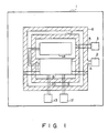
- Fig. 1 is a plan view showing a conventional multi-layer interconnect pattern.
- Reference numeral 1 denotes an IC chip whose power supplies V DD and GND are connected to a power supply pad 2 and ground pad 3, respectively, and are also connected to closed-loop patterns (power supply line patterns) 6 and 7, respectively, via a second metal layer (Al) 4 and first metal layer (Al) 5.
- the closed-loop patterns 6 and 7 are formed of the same material as that of the second metal layer (left-inclined hatched area in Fig. 1) in which case due consideration is paid to input/output signal lines 9, 10, and 11 coming from a logic block 8.
- the input/output signal lines 9, 10, and 11 coming from the logic block 8 are formed of the same material as the first metal layer (interconnect pattern without a hatched area) and provide a multi-level crossing relative to the power supply line patterns 6 and 7.
- Signal lines 9, 10, and 11 are connected to an input pad 12, output pad 13, and logic block 14, respectively.
- elements such as transistors
- the pattern width of the power supply lines 6 and 7 needs be broadened due to a need of more current flow in which case the size of the chip 1 is increased, for example, due to an increase in the number of transistors in the chip 1 and hence an increase in dissipation current in the chip 1.
- Such an increase in the size of the chip 1 results in an increase in the size of the interconnect area between the pad and the logic block and between the logic blocks.
- the object of the present invention is to solve the aforementioned drawbacks by providing a semiconductor device in which the area taken up by two or more types of power supply line within a semiconductor chip is reduced.
- a semiconductor device of a multi-layer structure wherein the element area required is reduced and a power supply line noise is reduced by a capacitor component between the power supply lines.
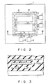
- Fig. 2 is a plan view of an interconnect pattern of a semiconductor device according to the embodiment of the present invention. Identical reference numerals are employed in Fig. 2 to designate parts or components corresponding to those shown in Fig. 1.
- closed-loop power supply line patterns 21 and 22 over a chip 1 are of such a type that a second metal layer (for example, Al) as indicated by a left-inclined hatched area and third metal layer (for example, Al) as indicated by right-inclined hatched area are independently and three-dimensionally formed in a superposed fashion in a plan view.
- a power supply V DD is connected to a power supply pad 2 and connected by, for example, a second metal layer 4 to the closed-loop power supply line pattern.
- a power supply GND is connected to the power supply pad 3 and connected by, for example, a third metal layer 5′ to the closed-loop power supply line pattern 22.
- Input/output signal lines 9 to 11 coming from a logic block 8 are formed of a first metal layer as indicated by a non-hatched area and provided, as a multi-level crossing, relative to the power supply lines 21 and 22.
- the input/output signal lines 9, 10, and 11 are connected to an input pad 12, output pad 13, and block 14, respectively.
- Fig. 3 is a cross-sectional view of the power supply line interconnect pattern area shown in Fig. 2.
- An input/output signal line 9 is formed as the first metal layer, this being the lowermost layer
- the power supply line pattern (V DD power supply) 21 is formed as the second metal layer, one level higher than that of the first metal layer
- the power supply line pattern 22 is formed as the third metal layer, or the topmost layer, over the second metal layer. Formed thus, the respective layers are not electrically connected to each other, since they are insulated from each other even if being connected in a multi-level fashion.
- the V DD power supply line 7 and GND power supply line 6, which are formed in parallel fashion with one of these power supply lines spaced from the other in a plan view in the conventional semiconductor device, can be superposed in a three-dimensional array, thus reducing the size of the pattern area as viewed from a plan view.
- the present invention when applied not only to a main power supply between the logic block and the pad but also to a main line between the logic blocks, obtains the same advantage as set forth above.
- the embodiment of the present invention has been explained in connection with the three-layer metal interconnect structure, the same advantage can be obtained if the structure has three or more layers.
- a plurality of metal interconnect layers may be employed for a single power supply.
- the metal interconnect layers 21 and 22 and signal interconnect layers 9 to 11 may be arranged one over another in a proper multi-level fashion.
Landscapes
- Internal Circuitry In Semiconductor Integrated Circuit Devices (AREA)
- Semiconductor Integrated Circuits (AREA)
- Design And Manufacture Of Integrated Circuits (AREA)
Applications Claiming Priority (2)
| Application Number | Priority Date | Filing Date | Title |
|---|---|---|---|
| JP63318245A JPH02163960A (ja) | 1988-12-16 | 1988-12-16 | 半導体装置 |
| JP318245/88 | 1988-12-16 |
Publications (2)
| Publication Number | Publication Date |
|---|---|
| EP0378809A2 true EP0378809A2 (fr) | 1990-07-25 |
| EP0378809A3 EP0378809A3 (fr) | 1990-12-12 |
Family
ID=18097054
Family Applications (1)
| Application Number | Title | Priority Date | Filing Date |
|---|---|---|---|
| EP19890123047 Withdrawn EP0378809A3 (fr) | 1988-12-16 | 1989-12-13 | Dispositif semi-conducteur comprenant une structure d'interconnexion à multicouche |
Country Status (4)
| Country | Link |
|---|---|
| US (1) | US5148263A (fr) |
| EP (1) | EP0378809A3 (fr) |
| JP (1) | JPH02163960A (fr) |
| KR (1) | KR940001285B1 (fr) |
Cited By (2)
| Publication number | Priority date | Publication date | Assignee | Title |
|---|---|---|---|---|
| EP0735584A3 (fr) * | 1995-03-30 | 1997-12-29 | AT&T Corp. | Technique d'interconnexion à niveaux multiples pour circuit intégré |
| EP1227517A2 (fr) | 2001-01-29 | 2002-07-31 | Sony Corporation | Dispositif semi-conducteur |
Families Citing this family (22)
| Publication number | Priority date | Publication date | Assignee | Title |
|---|---|---|---|---|
| US5216280A (en) * | 1989-12-02 | 1993-06-01 | Kabushiki Kaisha Toshiba | Semiconductor integrated circuit device having pads at periphery of semiconductor chip |
| US5446410A (en) * | 1992-04-20 | 1995-08-29 | Matsushita Electric Industrial Co.,Ltd. | Semiconductor integrated circuit |
| US5723908A (en) * | 1993-03-11 | 1998-03-03 | Kabushiki Kaisha Toshiba | Multilayer wiring structure |
| JPH07169807A (ja) * | 1993-12-16 | 1995-07-04 | Nippondenso Co Ltd | 半導体ウェハ |
| JP4027438B2 (ja) * | 1995-05-25 | 2007-12-26 | 三菱電機株式会社 | 半導体装置 |
| US5796265A (en) * | 1996-02-29 | 1998-08-18 | Lsi Logic Corporation | Method for metal delay testing in semiconductor devices |
| JPH1012825A (ja) * | 1996-06-26 | 1998-01-16 | Oki Electric Ind Co Ltd | 半導体集積回路装置 |
| JPH10284605A (ja) * | 1997-04-08 | 1998-10-23 | Mitsubishi Electric Corp | 半導体集積回路およびセルベース方式によりレイアウト設計された半導体集積回路 |
| US6255675B1 (en) | 1998-07-10 | 2001-07-03 | Xilinx, Inc. | Programmable capacitor for an integrated circuit |
| US6963510B1 (en) | 1998-07-10 | 2005-11-08 | Xilinx, Inc. | Programmable capacitor and method of operating same |
| JP3508837B2 (ja) * | 1999-12-10 | 2004-03-22 | インターナショナル・ビジネス・マシーンズ・コーポレーション | 液晶表示装置、液晶コントローラ、ビデオ信号伝送方法 |
| JP3727220B2 (ja) * | 2000-04-03 | 2005-12-14 | Necエレクトロニクス株式会社 | 半導体装置 |
| US6362972B1 (en) | 2000-04-13 | 2002-03-26 | Molex Incorporated | Contactless interconnection system |
| US6612852B1 (en) | 2000-04-13 | 2003-09-02 | Molex Incorporated | Contactless interconnection system |
| US6730946B2 (en) * | 2001-01-29 | 2004-05-04 | Sony Corporation | Semiconductor device |
| US6969909B2 (en) * | 2002-12-20 | 2005-11-29 | Vlt, Inc. | Flip chip FET device |
| US7038917B2 (en) * | 2002-12-27 | 2006-05-02 | Vlt, Inc. | Low loss, high density array interconnection |
| US7566964B2 (en) * | 2003-04-10 | 2009-07-28 | Agere Systems Inc. | Aluminum pad power bus and signal routing for integrated circuit devices utilizing copper technology interconnect structures |
| US20040251549A1 (en) * | 2003-06-11 | 2004-12-16 | Tai-Chun Huang | Hybrid copper/low k dielectric interconnect integration method and device |
| US7244673B2 (en) * | 2003-11-12 | 2007-07-17 | Taiwan Semiconductor Manufacturing Company, Ltd. | Integration film scheme for copper / low-k interconnect |
| US7161823B2 (en) | 2004-06-03 | 2007-01-09 | Samsung Electronics Co., Ltd. | Semiconductor memory device and method of arranging signal and power lines thereof |
| US8383952B2 (en) * | 2009-08-05 | 2013-02-26 | Kovio, Inc. | Printed compatible designs and layout schemes for printed electronics |
Family Cites Families (5)
| Publication number | Priority date | Publication date | Assignee | Title |
|---|---|---|---|---|
| JPS607147A (ja) * | 1983-06-24 | 1985-01-14 | Mitsubishi Electric Corp | 半導体装置 |
| JPS6146050A (ja) * | 1984-08-10 | 1986-03-06 | Nec Ic Microcomput Syst Ltd | 半導体集積回路装置 |
| JPS61218155A (ja) * | 1985-03-25 | 1986-09-27 | Hitachi Ltd | 半導体集積回路装置 |
| JPS6344742A (ja) * | 1986-08-12 | 1988-02-25 | Fujitsu Ltd | 半導体装置 |
| JPH073840B2 (ja) * | 1987-08-31 | 1995-01-18 | 株式会社東芝 | 半導体集積回路 |
-
1988
- 1988-12-16 JP JP63318245A patent/JPH02163960A/ja active Pending
-
1989
- 1989-12-13 EP EP19890123047 patent/EP0378809A3/fr not_active Withdrawn
- 1989-12-15 KR KR1019890018675A patent/KR940001285B1/ko not_active Expired - Fee Related
-
1991
- 1991-04-12 US US07/684,151 patent/US5148263A/en not_active Expired - Lifetime
Cited By (3)
| Publication number | Priority date | Publication date | Assignee | Title |
|---|---|---|---|---|
| EP0735584A3 (fr) * | 1995-03-30 | 1997-12-29 | AT&T Corp. | Technique d'interconnexion à niveaux multiples pour circuit intégré |
| EP1227517A2 (fr) | 2001-01-29 | 2002-07-31 | Sony Corporation | Dispositif semi-conducteur |
| EP1227517A3 (fr) * | 2001-01-29 | 2005-07-20 | Sony Corporation | Dispositif semi-conducteur |
Also Published As
| Publication number | Publication date |
|---|---|
| JPH02163960A (ja) | 1990-06-25 |
| EP0378809A3 (fr) | 1990-12-12 |
| US5148263A (en) | 1992-09-15 |
| KR940001285B1 (ko) | 1994-02-18 |
| KR900010999A (ko) | 1990-07-11 |
Similar Documents
| Publication | Publication Date | Title |
|---|---|---|
| EP0378809A2 (fr) | Dispositif semi-conducteur comprenant une structure d'interconnexion à multicouche | |
| US5885855A (en) | Method for distributing connection pads on a semiconductor die | |
| US6198635B1 (en) | Interconnect layout pattern for integrated circuit packages and the like | |
| US5543640A (en) | Logical three dimensional interconnections between integrated circuit chips using a two dimensional multi-chip module | |
| US5512765A (en) | Extendable circuit architecture | |
| EP0306620B1 (fr) | Structure de bus pour une puce de circuit intégré | |
| EP0074825B2 (fr) | Production de circuits intégrés par des méthodes à tranche maîtresse | |
| KR100282973B1 (ko) | 반도체장치 | |
| KR910000023B1 (ko) | 매스터 슬라이스형 집적회로 | |
| US6437431B1 (en) | Die power distribution system | |
| US5892276A (en) | Semiconductor integrated circuit | |
| US5258891A (en) | Multichip module with multilayer wiring substrate | |
| KR910003544B1 (ko) | 반도체장치 | |
| US4947233A (en) | Semi-custom LSI having input/output cells | |
| US6847120B2 (en) | Flip chip semiconductor device having signal pads arranged outside of power supply pads | |
| US6407462B1 (en) | Irregular grid bond pad layout arrangement for a flip chip package | |
| JPH0555380A (ja) | 半導体集積回路装置 | |
| US6956286B2 (en) | Integrated circuit package with overlapping bond fingers | |
| US6720636B2 (en) | Semiconductor device with a staggered pad arrangement | |
| US5063433A (en) | Semiconductor device having multi-layered wiring structure | |
| US5206529A (en) | Semiconductor integrated circuit device | |
| KR910007900B1 (ko) | 반도체 집적회로장치 | |
| US7266788B2 (en) | Via/BSM pattern optimization to reduce DC gradients and pin current density on single and multi-chip modules | |
| JPH07169840A (ja) | 半導体装置 | |
| JP3353410B2 (ja) | ゲートアレイの多層配線構造 |
Legal Events
| Date | Code | Title | Description |
|---|---|---|---|
| PUAI | Public reference made under article 153(3) epc to a published international application that has entered the european phase |
Free format text: ORIGINAL CODE: 0009012 |
|
| 17P | Request for examination filed |
Effective date: 19891213 |
|
| AK | Designated contracting states |
Kind code of ref document: A2 Designated state(s): DE FR GB |
|
| PUAL | Search report despatched |
Free format text: ORIGINAL CODE: 0009013 |
|
| AK | Designated contracting states |
Kind code of ref document: A3 Designated state(s): DE FR GB |
|
| 17Q | First examination report despatched |
Effective date: 19930820 |
|
| STAA | Information on the status of an ep patent application or granted ep patent |
Free format text: STATUS: THE APPLICATION IS DEEMED TO BE WITHDRAWN |
|
| 18D | Application deemed to be withdrawn |
Effective date: 19931231 |