EP0379301A1 - Méthode pour pelliculer un matériau organique - Google Patents
Méthode pour pelliculer un matériau organique Download PDFInfo
- Publication number
- EP0379301A1 EP0379301A1 EP90300282A EP90300282A EP0379301A1 EP 0379301 A1 EP0379301 A1 EP 0379301A1 EP 90300282 A EP90300282 A EP 90300282A EP 90300282 A EP90300282 A EP 90300282A EP 0379301 A1 EP0379301 A1 EP 0379301A1
- Authority
- EP
- European Patent Office
- Prior art keywords
- gas
- ashing
- plasma
- water
- oxygen
- Prior art date
- Legal status (The legal status is an assumption and is not a legal conclusion. Google has not performed a legal analysis and makes no representation as to the accuracy of the status listed.)
- Granted
Links
Images


Classifications
-
- H—ELECTRICITY
- H10—SEMICONDUCTOR DEVICES; ELECTRIC SOLID-STATE DEVICES NOT OTHERWISE PROVIDED FOR
- H10P—GENERIC PROCESSES OR APPARATUS FOR THE MANUFACTURE OR TREATMENT OF DEVICES COVERED BY CLASS H10
- H10P50/00—Etching of wafers, substrates or parts of devices
- H10P50/20—Dry etching; Plasma etching; Reactive-ion etching
- H10P50/28—Dry etching; Plasma etching; Reactive-ion etching of insulating materials
- H10P50/286—Dry etching; Plasma etching; Reactive-ion etching of insulating materials of organic materials
- H10P50/287—Dry etching; Plasma etching; Reactive-ion etching of insulating materials of organic materials by chemical means
-
- G—PHYSICS
- G03—PHOTOGRAPHY; CINEMATOGRAPHY; ANALOGOUS TECHNIQUES USING WAVES OTHER THAN OPTICAL WAVES; ELECTROGRAPHY; HOLOGRAPHY
- G03F—PHOTOMECHANICAL PRODUCTION OF TEXTURED OR PATTERNED SURFACES, e.g. FOR PRINTING, FOR PROCESSING OF SEMICONDUCTOR DEVICES; MATERIALS THEREFOR; ORIGINALS THEREFOR; APPARATUS SPECIALLY ADAPTED THEREFOR
- G03F7/00—Photomechanical, e.g. photolithographic, production of textured or patterned surfaces, e.g. printing surfaces; Materials therefor, e.g. comprising photoresists; Apparatus specially adapted therefor
- G03F7/26—Processing photosensitive materials; Apparatus therefor
- G03F7/42—Stripping or agents therefor
- G03F7/427—Stripping or agents therefor using plasma means only
-
- H—ELECTRICITY
- H01—ELECTRIC ELEMENTS
- H01J—ELECTRIC DISCHARGE TUBES OR DISCHARGE LAMPS
- H01J37/00—Discharge tubes with provision for introducing objects or material to be exposed to the discharge, e.g. for the purpose of examination or processing thereof
- H01J37/32—Gas-filled discharge tubes
- H01J37/32009—Arrangements for generation of plasma specially adapted for examination or treatment of objects, e.g. plasma sources
- H01J37/32082—Radio frequency generated discharge
-
- H—ELECTRICITY
- H01—ELECTRIC ELEMENTS
- H01J—ELECTRIC DISCHARGE TUBES OR DISCHARGE LAMPS
- H01J37/00—Discharge tubes with provision for introducing objects or material to be exposed to the discharge, e.g. for the purpose of examination or processing thereof
- H01J37/32—Gas-filled discharge tubes
- H01J37/32009—Arrangements for generation of plasma specially adapted for examination or treatment of objects, e.g. plasma sources
- H01J37/32192—Microwave generated discharge
-
- H—ELECTRICITY
- H01—ELECTRIC ELEMENTS
- H01J—ELECTRIC DISCHARGE TUBES OR DISCHARGE LAMPS
- H01J37/00—Discharge tubes with provision for introducing objects or material to be exposed to the discharge, e.g. for the purpose of examination or processing thereof
- H01J37/32—Gas-filled discharge tubes
- H01J37/32431—Constructional details of the reactor
- H01J37/3244—Gas supply means
-
- H—ELECTRICITY
- H01—ELECTRIC ELEMENTS
- H01J—ELECTRIC DISCHARGE TUBES OR DISCHARGE LAMPS
- H01J37/00—Discharge tubes with provision for introducing objects or material to be exposed to the discharge, e.g. for the purpose of examination or processing thereof
- H01J37/32—Gas-filled discharge tubes
- H01J37/32431—Constructional details of the reactor
- H01J37/32715—Workpiece holder
-
- H—ELECTRICITY
- H01—ELECTRIC ELEMENTS
- H01J—ELECTRIC DISCHARGE TUBES OR DISCHARGE LAMPS
- H01J37/00—Discharge tubes with provision for introducing objects or material to be exposed to the discharge, e.g. for the purpose of examination or processing thereof
- H01J37/32—Gas-filled discharge tubes
- H01J37/32431—Constructional details of the reactor
- H01J37/32798—Further details of plasma apparatus not provided for in groups H01J37/3244 - H01J37/32788; special provisions for cleaning or maintenance of the apparatus
- H01J37/32816—Pressure
- H01J37/32834—Exhausting
-
- H—ELECTRICITY
- H10—SEMICONDUCTOR DEVICES; ELECTRIC SOLID-STATE DEVICES NOT OTHERWISE PROVIDED FOR
- H10P—GENERIC PROCESSES OR APPARATUS FOR THE MANUFACTURE OR TREATMENT OF DEVICES COVERED BY CLASS H10
- H10P72/00—Handling or holding of wafers, substrates or devices during manufacture or treatment thereof
- H10P72/04—Apparatus for manufacture or treatment
- H10P72/0402—Apparatus for fluid treatment
Definitions
- the present invention relates to methods of stripping organic material, for example, to remove a resist such as a photoresist, X-ray resist, or electron beam resist, used in the production of semiconductor devices, liquid crystal devices and plasma displays.
- a resist such as a photoresist, X-ray resist, or electron beam resist
- a photoresist (hereinafter abbreviated as resist) is used as a mask when etching a wafer, and as the resist becomes unnecessary after the etching treatment, it must be removed.
- the removal methods include the wet treatment system in which a resist stripping solution is used, and the dry treatment system of oxydizing or ashing the resist in an active species of oxygen atoms or an oxygen plasma.
- a gas composed mainly of oxygen gas is used for the ashing.
- the wafer since the ashing rate (i.e., amount of organic material per unit of time) is low, the wafer must be heated to about 200°C or higher to obtain a satisfactory ashing rate.
- the wafer is thus heated, however, a minute amount of heavy metals and alkaline metals contained in the resist is introduced into the wafer, whereby problems relating to contamination of the wafer can arise.
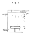
- FIG. 4 An apparatus for carrying out a downstream ashing method is shown in Fig. 4.
- a vacuum reaction chamber 6 is connected to the vacuum pump P, the reaction gases are fed through the gas introducing inlet 3 into the plasma generation chamber 4 provided in reaction chamber 6, and are then formed into a plasma by, for example, microwaves at a frequency of, for example, 2.45 GHz, transmitted through a microwave transmission window 2 by a waveguide 1.
- the ions and the electrons are shielded by the earthed shower head 5, and residual (neutral) active species pass through the shower head 5 and flow down toward the wafer 8 on the stage 7.
- the active species come into contact with the wafer 8 and remove the resist film, comprising an organic material (not shown) coated on the wafer 8, by ashing.
- a gas composed mainly of oxygen is introduced, as the gas for ashing, through the gas introducing inlet 3, formed into a plasma, and subjected to a downstream to bring the active species of oxygen atoms into contact with the wafer 8.
- the activation energy during the ashing is as high as 0.52 eV, the influence on the ashing rate of the temperature (i.e., temperature dependency) is great, and thus the reproducibility and controllability of the ashing are poor.
- the ashing rate is as low as 0.2 ⁇ m/min., and therefore, to obtaining the minimum limit of an about 0.5 ⁇ m/min. of ashing rate required for practical application, the wafer 8 must be heated to about 200°C or higher, and accordingly, the contamination problems of the wafer 8 arises.
- This method may be carried out using the apparatus of Fig. 4, by introducing O2 and H2O through the gas introducing inlet 3 to form the same into a plasma, which is then subjected to a downstream to bring active species of oxygen atoms formed from oxygen, oxygen atoms, and hydrogen atoms and OH formed from H2O, into contact with the wafer 8.
- Fig. 6 the relationship between the ratio of H2O to the total amount of the gas mixture of O2 and H2O is shown in Fig. 6. It should be noted that the stage temperature is 180°C, and the flow rate of the gas mixture of O2 and H2O is 1 liter/min.
- the ashing rate reaches a maximum value of 0.35 ⁇ m/min., which is about 2-fold that of the ashing method using a gas composed mainly of oxygen, when the content of H2O is 30% to 40%. Even when the ratio of H2O is further increased, the ashing rate is not substantially lowered.
- the activation energy is less, at 0.39 eV, compared with the ashing method using a gas composed mainly of oxygen. This is considered to be due to a lowering of the activation energy by OH formed primarily from H2O.
- the temperature dependency is reduced, and thus the reproducibility and controllability are improved.
- the wafer 8 must be heated to about 200°C or higher, and thus the contamination problems of the wafer still remains.
- an ashing rate of 1 ⁇ m/min. or higher which is about 5-fold higher than that of the method using a gas composed mainly of oxygen, can be obtained when about 10% to 15% of a gas containing a small amount of halogen, for example, carbon tetrafluoride (CF4) in oxygen, is added to the plasma.
- a gas containing a small amount of halogen for example, carbon tetrafluoride (CF4) in oxygen
- the gas containing a halogen promotes the dissociation of oxygen into oxygen atoms, when the gas containing oxygen and a halogen is formed into a plasma.
- the active species of oxygen atoms are increased, to improve the ashing rate, and at the same time, ashing at room temperature is possible due to a lowering of the activation energy by the action of fluorine, and further, an additional advantage is gained in that the temperature dependency is greatly reduced.
- the fluorine atoms reach the SiO2 surface, a drawback arises in that the substrate layer of, for example, SiO2, may be etched during the ashing process.
- a further method which can provide a satisfactory ashing rate even at room temperature, performs ashing by using a gas containing mainly fluorine, as described below:
- the method may be carried out in a modified downstream ashing apparatus such as that of Figure 5, which is an improved form of the apparatus of Fig. 4.
- This method comprises injecting NF3 through the gas introducing inlet 3 to form a plasma, and then subjecting the active species of fluorine atoms to a downstream through the shower plate 5.
- H2O is added in an amount smaller than the amount of NF3 injected, whereby the chemical reaction with fluorine and H2O, as shown below, occurs 2 F + H2O ⁇ 2HF + O to generate the oxygen atoms necessary for ashing.
- residual fluorine atoms which have not undergone the chemical reaction withdraw H from the C-H bond on the resist surface, thereby substituting for the H (H. Okano et al. The Electrochem. Soc. Spring Meeting, Atlanta, May 15 - 20, 1988).
- the ashing rate is improved by the oxygen atoms formed by the chemical reaction between the H2O and fluorine atoms, and the residual fluorine atoms, which have not undergone the chemical reaction. Further, the activation energy is lowered by a substitution of H from the C-H bond on the resist surface with fluorine atom, and accordingly, in addition to enabling ashing at room temperature, an advantage is gained in that the temperature dependency is greatly reduced.
- the wafer temperature In the first method described above, in which a gas composed mainly of oxygen is used, and in the method (a) (downstream ashing method with oxygen and water), the wafer temperature must be raised to 200°C or higher, to obtain a practical ashing rate, and thus the problem of wafer contamination can arise.
- a halogen-containing gas namely (b) the method of using a gas containing oxygen and a halogen, and (c) the method of adding water during the downstream of nitrogen trifluoride (NF3), because fluorine, which is a gas containing a halogen, is used to obtain a practical ashing rate even at room temperature, a problem can arise in that the substrate layer of, for example, SiO2, is etched.
- NF3 nitrogen trifluoride
- the above-described methods may not provide a satisfactory ashing rate at low temperature without etching the substrate layer, and without generating a contamination of the wafer.
- the substrate layer e.g. silicon dioxide, silicon nitride
- the substrate layer e.g. silicon dioxide, silicon nitride
- An embodiment of the present invention can provide a process for stripping an organic material, which comprises forming gases including a gas containing oxygen and a gas containing a halogen into plasma in a plasma chamber, and supplying an active species in the gas formed plasma to a reaction chamber to strip the organic material in the reaction chamber, wherein an amount of water vapor of at least one mole based upon two moles of the dissociated halogen atom is fed into the reaction chamber, and the active species of the halogen are removed before contact thereof with the organic material.
- the gas containing the halogen promotes dissociation of oxygen into free oxygen atoms, to increase the amount of free oxygen atoms.
- oxygen-containing gas are oxygen; air, and a mixture of oxygen with an inert gas, CO2 and /or N2.
- halogen-containing gas examples include F2, Cl2, Br2, HF, CF4, NF3, C2F6, C3F8, CHF3, SF6, CCl4, ClF3 , CCl2F2, C2ClF5, C2Cl2F4, CClF3 and Hbr, CBrF3, and xenon fluoride.
- the use of a fluorine-containing gas is preferable.
- the molar ratio of the halogen-containing gas/(the halogen-containing gas + the oxygen-containing gas) is preferably 0.05 to 0.3, more preferably 0.1 to 0.25.
- the active species in the gas formed into plasma are supplied to the vacuum reaction chamber 6, and water vapor is added in an amount of at least one mole, preferably 1.2 to 2.4 moles, for every 2 moles of the dissociated halogen atom (i.e., active species), during the course of the downward flow of the active species, the following chemical reaction occurs: 2 X + H2O ⁇ 2 HX + O.
- the active species of halogen formed by the halogen-containing gas which is utilized to promote a dissociation of oxygen, are substantially completely removed, and therefore, the substrate layer (e.g., SiO2, SiN) is not significantly etched.
- a part of the added water vapor is separated into oxygen atoms, hydrogen atoms, and OH by a secondary reaction with the active species in the downstream, to thereby increase the active species, and as a result, the amount of oxygen atoms and other active species participating in the ashing is increased, and thus the ashing rate is improved.
- the activation energy is lowered by the OH generated by the secondary reaction, whereby ashing at a lower temperature becomes possible, and further, the temperature dependency is reduced to thereby improve the reproducibility and controllability.
- the water vapor can be introduced into the reaction chamber by evacuating the content of a water vessel containing water.
- the water vessel can be optionally heated by a heater (e.g. an electric heater).
- the water vapor can also be introduced into the reaction chamber by bubbling the water in the water vessel with an inert carrier gas (e.g., N2, O2, H2, Ar, He).
- an inert carrier gas e.g., N2, O2, H2, Ar, He.
- a silicon wafer 8 having a diameter of 4 inches (about 10 cm) was used as the substrate of the sample to be ashed, a silicon wafer 8 having a diameter of 4 inches (about 10 cm) was used, a substrate layer of SiO2 is formed on the surface of the wafer 8 by the thermal oxidation method, and a resist of OFPR 800 (i.e., cresol-novolak resin type positive photoresist, a product of Tokyo Ohka K.K.), was then coated thereon by the spin coating method.
- OFPR 800 i.e., cresol-novolak resin type positive photoresist, a product of Tokyo Ohka K.K.
- the ashing process was carried out in the apparatus of Fig. 5, which has a plurality of water vapor inlets 9 capable of supplying water to be uniformly added to the reaction chamber 6, and the amounts of water supplied through the water vapor inlets 9 can be controlled.
- the other arrangements are similar to those as shown in Fig. 4.
- the pressure in the reaction vessel 6 is maintained at usually 0.1 to 3 Torr, typically about 0.8 Torr, and a microwave having a frequency of, for example, 2.45 GHz generated from a microwave generating device 11 is transmitted by a waveguide 1.
- a radio frequency can also be used instread of the microwave.
- gases for the ashing for example, oxygen and a small amount of CF4, introduced through the gas introducing inlet 3 from the bombs 12 and 13 through a mass flow controller 14, are used, and water in a saturated vapor preessure state is supplied through the water vapor inlet 9.
- the total amount of oxygen, CF4, and water at this time is controlled to one liter/min.
- the water vapor can be introduced by evacuating a water vessel 15 containing water 16 via a mass flow controller 14 or by bubbling an inert gas (e.g., N2) from a gas bomb or cylinder 18 via a mass flow controller 14.
- the water vessel 15 can be appropriately heated by a heater 17.
- the gases formed into a plasma are given a constant ratio of an amount of CF4 of 15% relative to the amount of a gas mixture of the oxygen and CF4.
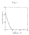
- the change in the SiO2 etching rate was determined when the added amount of water was varied from 0 to 30%.
- a sample having SiO2 formed on the whole surface of the wafer 8 as described above was used.
- the sample was mounted on a stage 7 having a temperature of 150°C, ashing was performed for 10 minutes, a measurement was conducted after ashing by a known esoprimetric method, and the SiO2 etching rate was obtained from the result of that measurement.
- the minimum limit of this measurement method is 5 ⁇ . The results are shown in Fig. 1.
- axis of the ordinate depicts the SiO2 etching rate
- the axis of the abscissa depicts the ratio of water relative to the total amount of oxygen, CF4, and water.
- the SiO2 When water was not added, the SiO2 was etched at an etching rate of about 230 ⁇ . As the added amount of water was increased, the etching rate was gradually lowered, and no etching of the SiO2 occurred when the added amount of water was more than about 10%.
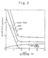
- a wafer 8 having a resist coated to a thickness of 1.1 ⁇ m on the surface thereof was used as the sample. After ashing of the sample for 30 seconds, the thickness of the resist was measured by a contact needle type step difference measuring instrument, and the ashing rate of the resist was calculated.
- axis of the ordinate depicts the ashing rate of the resist
- the axis of the abscissa depicts the ratio of water to the total amount of oxygen, CF4, and water.
- the ashing rate was very high, at 1 ⁇ m/min. or more, even when the temperature of the stage 7 was at room temperature, and thereafter, as the added amount of water was increased to about 10%, the ashing rate was lowered.
- the added amount of water exceeded about 10%, the ashing rate of a wafer at room temperature could not be measured, and the ashing rate became about 0.5 ⁇ m/min. and about 0.9 ⁇ m/min., at wafer temperatures of 150°C, and 180°C, respectively.
- the ashing rate which is about 0.9 ⁇ m/min. at a wafer temperature of 180°C, is lower than when the added amount of water is less than about 10%
- the ashing rate is improved about 5-fold compared with the method described above in which a gas composed mainly of oxygen is used, and about 2.5-fold compared with the method in which O2 + H2O are used as shown in Figure 4.
- the ashing rate is smaller when the added amount of water is about 10% or more than when it is smaller than about 10%. This may be considered to be due to an increased activation energy caused by the removal of fluorine atoms, and this can be readily estimated also from the tendency toward a change of the SiO2 etching rate shown in Fig. 1 with the added amount of water of 10% as the boundary, which is the same as the ashing rate tendency shown in the Fig. 1.
- the active species amount of oxygen atoms is increased by a generation of secondary oxygen atoms through the chemical reaction between water and fluorine, and further, oxygen atoms through the oxygen dissociation action of fluorine, and oxygen atoms and other active species through the secondary reaction can be obtained, the ashing rate is improved compared with the method in which O2 + H2O are used.
- the activation energy at this time was determined as described below.
- a wafer 8 surface coated with a resist to a thickness of 1.1 ⁇ m was used as the sample.
- the sample was mounted on the stage, and after ashing was performed by varying the stage temperature at predetermined temperature intervals each time the added amount of water was varied, the thickness of the resist was measured by a contact needle type step difference measuring instrument, and the ashing rate of the resist was calculated.
- the activation energy was determined from the slope of the straight line.
- the Fig. 3 the activation energy is shown on the logarithmic scale on the axis of the ordinate, and the ratio of water relative to the total amount of oxygen, CF4, and water on the axis of the abscissa.
- the activation energy was as low as 0.05 eV, due to the influence of the fluorine atoms. Subsequently, as the added amount of water was increased to about 10%, the activation energy became higher, until at about 10% or higher, the activation energy became stabilized at about 0.39 eV, as in the downstream ashing method in which oxygen and water were used.
- This phenomenon is understood to be due to the fact that, if the added amount of water is about 10% or more, fluorine atoms can be removed to eliminate the influence of the fluorine, whereby OH formed from water by a secondary reaction mainly determines the activation energy.
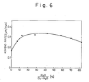
- water is added in an amount larger than that of the active species of fluorine atoms. That is, when the ratio of CF4 relative to the amount of the gas mixture of oxygen and CF4 is 15%, ashing is performed with the added amount of water of about 10% or more.
- OH formed by a separation of water lowers the activation energy to 0.39 eV, which is less than the 0.52 eV obtained in the method described above in which a gas composed mainly of oxygen is used, and thus in addition to enabling ashing at a lower temperature, the temperature dependency is reduced and the reproducibility and controllability are accordingly enhanced.
- the ashing rate was about 10,000 ⁇ /min.
- the ashing rate was about 7,500 ⁇ /min. Thus, about 33% increase in the ashing rate was attained by the above process embodying the invention.
- the process in this Example is not limited to the ashing of a resist, but also can be applied to the oxidation and ashing of a large number of organic materials other than a resist.
- CF4 was employed as the gas for ashing, similar effects can be obtained even when the other fluorine-containing gases (e.g., C2F6 and NF3), which are fluorinated gases, are employed, and a gas containing a halogen also may be used.
- the number of oxygen atoms participating in the ashing can be increased and substantially all halogen atoms are removed before they reach the wafer, and further, the reproducibility and controllability are enhanced by lowering the activation energy to thereby reduce the temperature dependency. Accordingly, a high ashing rate can be achieved at a desirably low temperature, without unacceptable etching of the substrate layer, thereby assisting in the production of substantially undamaged semiconductor devices.
Landscapes
- Physics & Mathematics (AREA)
- Engineering & Computer Science (AREA)
- Plasma & Fusion (AREA)
- Chemical & Material Sciences (AREA)
- Analytical Chemistry (AREA)
- General Physics & Mathematics (AREA)
- Drying Of Semiconductors (AREA)
- Exposure Of Semiconductors, Excluding Electron Or Ion Beam Exposure (AREA)
Applications Claiming Priority (2)
| Application Number | Priority Date | Filing Date | Title |
|---|---|---|---|
| JP3303/89 | 1989-01-10 | ||
| JP1003303A JP2890432B2 (ja) | 1989-01-10 | 1989-01-10 | 有機物の灰化方法 |
Publications (2)
| Publication Number | Publication Date |
|---|---|
| EP0379301A1 true EP0379301A1 (fr) | 1990-07-25 |
| EP0379301B1 EP0379301B1 (fr) | 1995-11-08 |
Family
ID=11553594
Family Applications (1)
| Application Number | Title | Priority Date | Filing Date |
|---|---|---|---|
| EP90300282A Expired - Lifetime EP0379301B1 (fr) | 1989-01-10 | 1990-01-10 | Méthode pour pelliculer un matériau organique |
Country Status (5)
| Country | Link |
|---|---|
| US (1) | US4983254A (fr) |
| EP (1) | EP0379301B1 (fr) |
| JP (1) | JP2890432B2 (fr) |
| KR (1) | KR940001646B1 (fr) |
| DE (1) | DE69023355D1 (fr) |
Cited By (8)
| Publication number | Priority date | Publication date | Assignee | Title |
|---|---|---|---|---|
| WO1991001516A3 (fr) * | 1989-07-21 | 1991-04-18 | Univ Texas | Procedes de formation et de transfert de configurations |
| WO1993015444A1 (fr) * | 1992-01-30 | 1993-08-05 | Fraunhofer-Gesellschaft zur Förderung der angewandten Forschung e.V. | Procede de developpement a sec d'une couche de vernis a teneur en silicium, sensible aux rayons ultraviolets et/ou aux faisceaux d'electrons |
| WO1995022171A3 (fr) * | 1994-02-03 | 1995-09-08 | Applied Materials Inc | Decapage, passivation et inhibition de la corrosion de substrats a semi-conducteurs |
| US5545289A (en) * | 1994-02-03 | 1996-08-13 | Applied Materials, Inc. | Passivating, stripping and corrosion inhibition of semiconductor substrates |
| EP0798767A3 (fr) * | 1996-03-29 | 1998-03-11 | Praxair Technology, Inc. | Elimination de carbone de la surface de substrats |
| EP0940846A1 (fr) * | 1998-03-06 | 1999-09-08 | Interuniversitair Micro-Elektronica Centrum Vzw | Méthode de retrait d'un photorésiste ayant subi une implantation ionique |
| US6440864B1 (en) | 2000-06-30 | 2002-08-27 | Applied Materials Inc. | Substrate cleaning process |
| US6692903B2 (en) | 2000-12-13 | 2004-02-17 | Applied Materials, Inc | Substrate cleaning apparatus and method |
Families Citing this family (43)
| Publication number | Priority date | Publication date | Assignee | Title |
|---|---|---|---|---|
| JPH0777211B2 (ja) * | 1987-08-19 | 1995-08-16 | 富士通株式会社 | アッシング方法 |
| US5226056A (en) * | 1989-01-10 | 1993-07-06 | Nihon Shinku Gijutsu Kabushiki Kaisha | Plasma ashing method and apparatus therefor |
| EP0416774B1 (fr) * | 1989-08-28 | 2000-11-15 | Hitachi, Ltd. | Procédé de traitement d'un échantillon de matériau contenant de l'aluminium |
| US5228052A (en) * | 1991-09-11 | 1993-07-13 | Nihon Shinku Gijutsu Kabushiki Kaisha | Plasma ashing apparatus |
| DE4132559A1 (de) * | 1991-09-30 | 1993-04-08 | Siemens Ag | Verfahren zur in-situ-reinigung von abscheidekammern durch plasmaaetzen |
| DE4202158C1 (fr) * | 1992-01-27 | 1993-07-22 | Siemens Ag, 8000 Muenchen, De | |
| JP3502096B2 (ja) * | 1992-06-22 | 2004-03-02 | ラム リサーチ コーポレイション | プラズマ処理装置内の残留物を除去するためのプラズマクリーニング方法 |
| US5387289A (en) * | 1992-09-22 | 1995-02-07 | Genus, Inc. | Film uniformity by selective pressure gradient control |
| JP3231426B2 (ja) * | 1992-10-28 | 2001-11-19 | 富士通株式会社 | 水素プラズマダウンフロー処理方法及び水素プラズマダウンフロー処理装置 |
| US5445679A (en) * | 1992-12-23 | 1995-08-29 | Memc Electronic Materials, Inc. | Cleaning of polycrystalline silicon for charging into a Czochralski growing process |
| DE4308990A1 (de) * | 1993-03-20 | 1994-09-22 | Bosch Gmbh Robert | Ätzverfahren und Vorrichtung zur Reinigung von Halbleiterelementen, insbesondere Leistungsdioden |
| JPH06285868A (ja) * | 1993-03-30 | 1994-10-11 | Bridgestone Corp | 加硫金型の清浄方法 |
| JP2804700B2 (ja) * | 1993-03-31 | 1998-09-30 | 富士通株式会社 | 半導体装置の製造装置及び半導体装置の製造方法 |
| JP3288490B2 (ja) * | 1993-07-09 | 2002-06-04 | 富士通株式会社 | 半導体装置の製造方法及び半導体装置の製造装置 |
| JP3438109B2 (ja) * | 1994-08-12 | 2003-08-18 | 富士通株式会社 | プラズマ処理装置及びプラズマ処理方法 |
| JPH08186098A (ja) * | 1994-12-27 | 1996-07-16 | Ryoden Semiconductor Syst Eng Kk | 感光性樹脂の除去方法および除去装置 |
| US5671116A (en) * | 1995-03-10 | 1997-09-23 | Lam Research Corporation | Multilayered electrostatic chuck and method of manufacture thereof |
| US5753567A (en) * | 1995-08-28 | 1998-05-19 | Memc Electronic Materials, Inc. | Cleaning of metallic contaminants from the surface of polycrystalline silicon with a halogen gas or plasma |
| US5835333A (en) * | 1995-10-30 | 1998-11-10 | Lam Research Corporation | Negative offset bipolar electrostatic chucks |
| US5693147A (en) * | 1995-11-03 | 1997-12-02 | Motorola, Inc. | Method for cleaning a process chamber |
| US5780359A (en) * | 1995-12-11 | 1998-07-14 | Applied Materials, Inc. | Polymer removal from top surfaces and sidewalls of a semiconductor wafer |
| US5614026A (en) * | 1996-03-29 | 1997-03-25 | Lam Research Corporation | Showerhead for uniform distribution of process gas |
| US5812361A (en) * | 1996-03-29 | 1998-09-22 | Lam Research Corporation | Dynamic feedback electrostatic wafer chuck |
| JPH09270421A (ja) | 1996-04-01 | 1997-10-14 | Mitsubishi Electric Corp | 表面処理装置および表面処理方法 |
| US6015761A (en) * | 1996-06-26 | 2000-01-18 | Applied Materials, Inc. | Microwave-activated etching of dielectric layers |
| US5925577A (en) * | 1997-02-19 | 1999-07-20 | Vlsi Technology, Inc. | Method for forming via contact hole in a semiconductor device |
| US7001848B1 (en) * | 1997-11-26 | 2006-02-21 | Texas Instruments Incorporated | Hydrogen plasma photoresist strip and polymeric residue cleanup process for oxygen-sensitive materials |
| US6080680A (en) * | 1997-12-19 | 2000-06-27 | Lam Research Corporation | Method and composition for dry etching in semiconductor fabrication |
| US6387819B1 (en) * | 1998-04-29 | 2002-05-14 | Applied Materials, Inc. | Method for etching low K dielectric layers |
| US6410417B1 (en) * | 1998-11-05 | 2002-06-25 | Promos Technologies, Inc. | Method of forming tungsten interconnect and vias without tungsten loss during wet stripping of photoresist polymer |
| US6599829B2 (en) | 1998-11-25 | 2003-07-29 | Texas Instruments Incorporated | Method for photoresist strip, sidewall polymer removal and passivation for aluminum metallization |
| US6242350B1 (en) | 1999-03-18 | 2001-06-05 | Taiwan Semiconductor Manufacturing Company | Post gate etch cleaning process for self-aligned gate mosfets |
| US6610168B1 (en) * | 1999-08-12 | 2003-08-26 | Sipec Corporation | Resist film removal apparatus and resist film removal method |
| US6805139B1 (en) | 1999-10-20 | 2004-10-19 | Mattson Technology, Inc. | Systems and methods for photoresist strip and residue treatment in integrated circuit manufacturing |
| US20050022839A1 (en) * | 1999-10-20 | 2005-02-03 | Savas Stephen E. | Systems and methods for photoresist strip and residue treatment in integrated circuit manufacturing |
| US6440874B1 (en) * | 2000-03-24 | 2002-08-27 | Advanced Micro Devices, Inc. | High throughput plasma resist strip process for temperature sensitive applications |
| CN1461493A (zh) * | 2000-12-18 | 2003-12-10 | 住友精密工业株式会社 | 清洗方法和腐蚀方法 |
| JP2006019414A (ja) * | 2004-06-30 | 2006-01-19 | Canon Inc | プラズマ処理装置 |
| US20070186953A1 (en) * | 2004-07-12 | 2007-08-16 | Savas Stephen E | Systems and Methods for Photoresist Strip and Residue Treatment in Integrated Circuit Manufacturing |
| US20070123049A1 (en) * | 2005-11-17 | 2007-05-31 | Kao-Su Huang | Semiconductor process and method for removing condensed gaseous etchant residues on wafer |
| JP4946321B2 (ja) * | 2006-09-29 | 2012-06-06 | 富士通セミコンダクター株式会社 | 基板処理装置及び基板処理方法 |
| US20080296258A1 (en) * | 2007-02-08 | 2008-12-04 | Elliott David J | Plenum reactor system |
| TWI576938B (zh) | 2012-08-17 | 2017-04-01 | 斯克林集團公司 | 基板處理裝置及基板處理方法 |
Citations (3)
| Publication number | Priority date | Publication date | Assignee | Title |
|---|---|---|---|---|
| EP0237078A2 (fr) * | 1986-03-13 | 1987-09-16 | Fujitsu Limited | Appareil de traitement en aval par plasma micro-onde comportant une structure de couplage entre la micro-onde et le plasma |
| EP0328350A2 (fr) * | 1988-02-09 | 1989-08-16 | Fujitsu Limited | Attaque sèche avec du bromure d'hydrogène ou du brome |
| EP0345757A2 (fr) * | 1988-06-09 | 1989-12-13 | Fujitsu Limited | Enlèvement d'une couche organique sur un dispositif semi-conducteur pendant sa fabrication par réduction en cendres |
Family Cites Families (3)
| Publication number | Priority date | Publication date | Assignee | Title |
|---|---|---|---|---|
| US4699689A (en) * | 1985-05-17 | 1987-10-13 | Emergent Technologies Corporation | Method and apparatus for dry processing of substrates |
| US4749440A (en) * | 1985-08-28 | 1988-06-07 | Fsi Corporation | Gaseous process and apparatus for removing films from substrates |
| JPH02174120A (ja) * | 1988-12-27 | 1990-07-05 | Toshiba Corp | 有機高分子膜の除去方法 |
-
1989
- 1989-01-10 JP JP1003303A patent/JP2890432B2/ja not_active Expired - Lifetime
-
1990
- 1990-01-04 US US07/460,798 patent/US4983254A/en not_active Expired - Lifetime
- 1990-01-10 EP EP90300282A patent/EP0379301B1/fr not_active Expired - Lifetime
- 1990-01-10 DE DE69023355T patent/DE69023355D1/de not_active Expired - Lifetime
- 1990-01-10 KR KR1019900000240A patent/KR940001646B1/ko not_active Expired - Lifetime
Patent Citations (3)
| Publication number | Priority date | Publication date | Assignee | Title |
|---|---|---|---|---|
| EP0237078A2 (fr) * | 1986-03-13 | 1987-09-16 | Fujitsu Limited | Appareil de traitement en aval par plasma micro-onde comportant une structure de couplage entre la micro-onde et le plasma |
| EP0328350A2 (fr) * | 1988-02-09 | 1989-08-16 | Fujitsu Limited | Attaque sèche avec du bromure d'hydrogène ou du brome |
| EP0345757A2 (fr) * | 1988-06-09 | 1989-12-13 | Fujitsu Limited | Enlèvement d'une couche organique sur un dispositif semi-conducteur pendant sa fabrication par réduction en cendres |
Non-Patent Citations (5)
| Title |
|---|
| 4EME COLLOQUE INTERNATIONAL SUR LES PLASMAS ET LA PULVERISATION CATHODIQUE, Nice, 13th-17th September 1982, pages 79-87, Paris, FR; G. TURBAN et al.: "Gravure du polyimide kapton H dans les plasmas oxyfluores" * |
| EXTENDED ABSTRACTS/SPRING MEETING, vol. 88-1, 15th-20th May 1988, pages 159-160, Princeton, NY, US; H. OKANO et al.: "Down-flow type resist ashing technique employing reaction of fluorine atoms to water vapor" * |
| PATENT ABSTRACTS OF JAPAN, vol. 13, no. 248 (E-770), 6th June 1989; & JP-A-01 048 421 (FUJITSU LTD) 22-02-1989 * |
| PATENT ABSTRACTS OF JAPAN, vol. 13, no. 268 (E-775), 20th June 1989; & JP-A-01 059 819 (TOKUDO SEISAKUSHO) 07-03-1989 * |
| PATENT ABSTRACTS OF JAPAN, vol. 13, no. 5 (E-701), 9th January 1989; & JP-A-63 217 629 (HITACHI LTD) 09-09-1988 * |
Cited By (10)
| Publication number | Priority date | Publication date | Assignee | Title |
|---|---|---|---|---|
| WO1991001516A3 (fr) * | 1989-07-21 | 1991-04-18 | Univ Texas | Procedes de formation et de transfert de configurations |
| US5178989A (en) * | 1989-07-21 | 1993-01-12 | Board Of Regents, The University Of Texas System | Pattern forming and transferring processes |
| WO1993015444A1 (fr) * | 1992-01-30 | 1993-08-05 | Fraunhofer-Gesellschaft zur Förderung der angewandten Forschung e.V. | Procede de developpement a sec d'une couche de vernis a teneur en silicium, sensible aux rayons ultraviolets et/ou aux faisceaux d'electrons |
| WO1995022171A3 (fr) * | 1994-02-03 | 1995-09-08 | Applied Materials Inc | Decapage, passivation et inhibition de la corrosion de substrats a semi-conducteurs |
| US5545289A (en) * | 1994-02-03 | 1996-08-13 | Applied Materials, Inc. | Passivating, stripping and corrosion inhibition of semiconductor substrates |
| EP0798767A3 (fr) * | 1996-03-29 | 1998-03-11 | Praxair Technology, Inc. | Elimination de carbone de la surface de substrats |
| US6352936B1 (en) | 1998-02-27 | 2002-03-05 | Imec Vzw | Method for stripping ion implanted photoresist layer |
| EP0940846A1 (fr) * | 1998-03-06 | 1999-09-08 | Interuniversitair Micro-Elektronica Centrum Vzw | Méthode de retrait d'un photorésiste ayant subi une implantation ionique |
| US6440864B1 (en) | 2000-06-30 | 2002-08-27 | Applied Materials Inc. | Substrate cleaning process |
| US6692903B2 (en) | 2000-12-13 | 2004-02-17 | Applied Materials, Inc | Substrate cleaning apparatus and method |
Also Published As
| Publication number | Publication date |
|---|---|
| DE69023355D1 (de) | 1995-12-14 |
| EP0379301B1 (fr) | 1995-11-08 |
| KR900012333A (ko) | 1990-08-03 |
| US4983254A (en) | 1991-01-08 |
| JPH02183528A (ja) | 1990-07-18 |
| JP2890432B2 (ja) | 1999-05-17 |
| KR940001646B1 (ko) | 1994-02-28 |
Similar Documents
| Publication | Publication Date | Title |
|---|---|---|
| EP0379301B1 (fr) | Méthode pour pelliculer un matériau organique | |
| US6060400A (en) | Highly selective chemical dry etching of silicon nitride over silicon and silicon dioxide | |
| EP0345757B1 (fr) | Enlèvement d'une couche organique sur un dispositif semi-conducteur pendant sa fabrication par réduction en cendres | |
| US9299581B2 (en) | Methods of dry stripping boron-carbon films | |
| US5157000A (en) | Method for dry etching openings in integrated circuit layers | |
| US10510518B2 (en) | Methods of dry stripping boron-carbon films | |
| JP3084497B2 (ja) | SiO2膜のエッチング方法 | |
| CN101983417B (zh) | 等离子体蚀刻方法 | |
| US5188704A (en) | Selective silicon nitride plasma etching | |
| SG193093A1 (en) | Method for etching organic hardmasks | |
| Fujimura et al. | Resist stripping in an O2+ H2O plasma downstream | |
| EP0424299A2 (fr) | Gravure sélective de plasma de nitrium de silicium | |
| JPS59100539A (ja) | 半導体装置の製造方法 | |
| KR20190077545A (ko) | 급속 열 활성화 공정과 함께 플라즈마를 이용하는 원자층 에칭 공정 | |
| US5017511A (en) | Method for dry etching vias in integrated circuit layers | |
| US5304514A (en) | Dry etching method | |
| US7244313B1 (en) | Plasma etch and photoresist strip process with intervening chamber de-fluorination and wafer de-fluorination steps | |
| JPH07169754A (ja) | 半導体装置のエッチング損傷を減少させるための方法 | |
| JP3563214B2 (ja) | プラズマエッチング方法 | |
| Bell et al. | Radiation damage to thermal silicon dioxide films in radio frequency and microwave downstream photoresist stripping systems | |
| JP3124599B2 (ja) | エッチング方法 | |
| JP3963295B2 (ja) | ケミカルドライエッチング方法 | |
| CN113053744B (zh) | 半导体装置的制造方法 | |
| US11756793B2 (en) | Semiconductor device manufacturing method | |
| JPS5855568A (ja) | 反応性イオンエツチング方法 |
Legal Events
| Date | Code | Title | Description |
|---|---|---|---|
| PUAI | Public reference made under article 153(3) epc to a published international application that has entered the european phase |
Free format text: ORIGINAL CODE: 0009012 |
|
| AK | Designated contracting states |
Kind code of ref document: A1 Designated state(s): DE FR GB |
|
| 17P | Request for examination filed |
Effective date: 19901228 |
|
| 17Q | First examination report despatched |
Effective date: 19930429 |
|
| GRAA | (expected) grant |
Free format text: ORIGINAL CODE: 0009210 |
|
| AK | Designated contracting states |
Kind code of ref document: B1 Designated state(s): DE FR GB |
|
| REF | Corresponds to: |
Ref document number: 69023355 Country of ref document: DE Date of ref document: 19951214 |
|
| PG25 | Lapsed in a contracting state [announced via postgrant information from national office to epo] |
Ref country code: GB Effective date: 19960208 |
|
| PG25 | Lapsed in a contracting state [announced via postgrant information from national office to epo] |
Ref country code: DE Effective date: 19960209 |
|
| ET | Fr: translation filed | ||
| PLBE | No opposition filed within time limit |
Free format text: ORIGINAL CODE: 0009261 |
|
| STAA | Information on the status of an ep patent application or granted ep patent |
Free format text: STATUS: NO OPPOSITION FILED WITHIN TIME LIMIT |
|
| GBPC | Gb: european patent ceased through non-payment of renewal fee |
Effective date: 19960208 |
|
| 26N | No opposition filed | ||
| REG | Reference to a national code |
Ref country code: FR Ref legal event code: TP |
|
| PGFP | Annual fee paid to national office [announced via postgrant information from national office to epo] |
Ref country code: FR Payment date: 20090113 Year of fee payment: 20 |