EP0379349A2 - Elément de conversion photoélectrique - Google Patents
Elément de conversion photoélectrique Download PDFInfo
- Publication number
- EP0379349A2 EP0379349A2 EP90300474A EP90300474A EP0379349A2 EP 0379349 A2 EP0379349 A2 EP 0379349A2 EP 90300474 A EP90300474 A EP 90300474A EP 90300474 A EP90300474 A EP 90300474A EP 0379349 A2 EP0379349 A2 EP 0379349A2
- Authority
- EP
- European Patent Office
- Prior art keywords
- photoelectric conversion
- conversion unit
- electrode area
- layer
- spectral sensitivity
- Prior art date
- Legal status (The legal status is an assumption and is not a legal conclusion. Google has not performed a legal analysis and makes no representation as to the accuracy of the status listed.)
- Withdrawn
Links
- 238000006243 chemical reaction Methods 0.000 title claims abstract description 126
- 230000035945 sensitivity Effects 0.000 claims abstract description 27
- 230000003595 spectral effect Effects 0.000 claims abstract description 26
- 238000000034 method Methods 0.000 claims abstract description 14
- 238000012545 processing Methods 0.000 claims abstract description 12
- 229910021417 amorphous silicon Inorganic materials 0.000 claims description 16
- 239000000463 material Substances 0.000 claims description 14
- 239000000969 carrier Substances 0.000 claims description 10
- 239000004065 semiconductor Substances 0.000 claims description 9
- 239000000203 mixture Substances 0.000 claims description 6
- 229910000577 Silicon-germanium Inorganic materials 0.000 claims description 4
- 230000000903 blocking effect Effects 0.000 claims description 4
- 230000005669 field effect Effects 0.000 claims description 3
- 229910052710 silicon Inorganic materials 0.000 claims description 3
- 239000010703 silicon Substances 0.000 claims description 3
- 239000000470 constituent Substances 0.000 claims description 2
- 238000000926 separation method Methods 0.000 claims 1
- 239000010410 layer Substances 0.000 description 105
- 229910021420 polycrystalline silicon Inorganic materials 0.000 description 12
- 238000012546 transfer Methods 0.000 description 11
- 229910010271 silicon carbide Inorganic materials 0.000 description 9
- 239000000758 substrate Substances 0.000 description 7
- 238000009825 accumulation Methods 0.000 description 4
- 238000000151 deposition Methods 0.000 description 4
- 238000010586 diagram Methods 0.000 description 4
- 239000012535 impurity Substances 0.000 description 4
- 230000003647 oxidation Effects 0.000 description 4
- 238000007254 oxidation reaction Methods 0.000 description 4
- 239000003990 capacitor Substances 0.000 description 3
- 230000007423 decrease Effects 0.000 description 3
- 150000002500 ions Chemical class 0.000 description 3
- 238000001020 plasma etching Methods 0.000 description 3
- BLRPTPMANUNPDV-UHFFFAOYSA-N Silane Chemical compound [SiH4] BLRPTPMANUNPDV-UHFFFAOYSA-N 0.000 description 2
- VYPSYNLAJGMNEJ-UHFFFAOYSA-N Silicium dioxide Chemical group O=[Si]=O VYPSYNLAJGMNEJ-UHFFFAOYSA-N 0.000 description 2
- XUIMIQQOPSSXEZ-UHFFFAOYSA-N Silicon Chemical compound [Si] XUIMIQQOPSSXEZ-UHFFFAOYSA-N 0.000 description 2
- 238000000137 annealing Methods 0.000 description 2
- 230000004888 barrier function Effects 0.000 description 2
- 230000008021 deposition Effects 0.000 description 2
- 238000009792 diffusion process Methods 0.000 description 2
- 239000011229 interlayer Substances 0.000 description 2
- 238000004519 manufacturing process Methods 0.000 description 2
- 230000001681 protective effect Effects 0.000 description 2
- 229910052814 silicon oxide Inorganic materials 0.000 description 2
- 230000004304 visual acuity Effects 0.000 description 2
- 241000293849 Cordylanthus Species 0.000 description 1
- UFHFLCQGNIYNRP-UHFFFAOYSA-N Hydrogen Chemical compound [H][H] UFHFLCQGNIYNRP-UHFFFAOYSA-N 0.000 description 1
- OAICVXFJPJFONN-UHFFFAOYSA-N Phosphorus Chemical compound [P] OAICVXFJPJFONN-UHFFFAOYSA-N 0.000 description 1
- 229910018540 Si C Inorganic materials 0.000 description 1
- 229910007161 Si(CH3)3 Inorganic materials 0.000 description 1
- ATJFFYVFTNAWJD-UHFFFAOYSA-N Tin Chemical compound [Sn] ATJFFYVFTNAWJD-UHFFFAOYSA-N 0.000 description 1
- 229910017875 a-SiN Inorganic materials 0.000 description 1
- 229910052782 aluminium Inorganic materials 0.000 description 1
- XAGFODPZIPBFFR-UHFFFAOYSA-N aluminium Chemical compound [Al] XAGFODPZIPBFFR-UHFFFAOYSA-N 0.000 description 1
- 230000005540 biological transmission Effects 0.000 description 1
- 230000015572 biosynthetic process Effects 0.000 description 1
- 239000003086 colorant Substances 0.000 description 1
- 238000013461 design Methods 0.000 description 1
- 230000005684 electric field Effects 0.000 description 1
- 238000005530 etching Methods 0.000 description 1
- 238000002474 experimental method Methods 0.000 description 1
- 125000005843 halogen group Chemical group 0.000 description 1
- 238000010438 heat treatment Methods 0.000 description 1
- 229910052739 hydrogen Inorganic materials 0.000 description 1
- 239000001257 hydrogen Substances 0.000 description 1
- 238000002347 injection Methods 0.000 description 1
- 239000007924 injection Substances 0.000 description 1
- 230000010354 integration Effects 0.000 description 1
- 229910052740 iodine Inorganic materials 0.000 description 1
- 238000005468 ion implantation Methods 0.000 description 1
- 229910052751 metal Inorganic materials 0.000 description 1
- 239000002184 metal Substances 0.000 description 1
- 150000004767 nitrides Chemical class 0.000 description 1
- 229910052757 nitrogen Inorganic materials 0.000 description 1
- 238000000059 patterning Methods 0.000 description 1
- 229910052698 phosphorus Inorganic materials 0.000 description 1
- 229920002120 photoresistant polymer Polymers 0.000 description 1
- 238000005268 plasma chemical vapour deposition Methods 0.000 description 1
- 239000011347 resin Substances 0.000 description 1
- 229920005989 resin Polymers 0.000 description 1
- 238000007789 sealing Methods 0.000 description 1
- SBIBMFFZSBJNJF-UHFFFAOYSA-N selenium;zinc Chemical compound [Se]=[Zn] SBIBMFFZSBJNJF-UHFFFAOYSA-N 0.000 description 1
- HBMJWWWQQXIZIP-UHFFFAOYSA-N silicon carbide Chemical compound [Si+]#[C-] HBMJWWWQQXIZIP-UHFFFAOYSA-N 0.000 description 1
- 239000002356 single layer Substances 0.000 description 1
- 238000004544 sputter deposition Methods 0.000 description 1
- 238000002834 transmittance Methods 0.000 description 1
Images





Classifications
-
- H—ELECTRICITY
- H10—SEMICONDUCTOR DEVICES; ELECTRIC SOLID-STATE DEVICES NOT OTHERWISE PROVIDED FOR
- H10F—INORGANIC SEMICONDUCTOR DEVICES SENSITIVE TO INFRARED RADIATION, LIGHT, ELECTROMAGNETIC RADIATION OF SHORTER WAVELENGTH OR CORPUSCULAR RADIATION
- H10F39/00—Integrated devices, or assemblies of multiple devices, comprising at least one element covered by group H10F30/00, e.g. radiation detectors comprising photodiode arrays
- H10F39/10—Integrated devices
- H10F39/12—Image sensors
- H10F39/18—Complementary metal-oxide-semiconductor [CMOS] image sensors; Photodiode array image sensors
- H10F39/182—Colour image sensors
Definitions
- the present invention relates to a photoelectric conversion device adapted for use in an image reader for example of a copying machine or a facsimile apparatus or as an image sensor of a video camera, and more particularly a photoelectric conversion device for color image reading, without light loss and residual image.
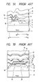
- Fig. 1A is a cross-sectional view of an example of a photoelectric converting area of a conventional color MOS solid-state image sensor (for example reported in an article "MOS solid-state image sensors commercialized in color video cameras", S. Nagahara, Optronics (1092) No. 3, p. 15 - 21).
- Fig. 1A is a cross-sectional view of an example of a photoelectric converting area of a conventional color MOS solid-state image sensor (for example reported in an article "MOS solid-state image sensors commercialized in color video cameras", S. Nagahara, Optronics (1092) No. 3, p. 15 - 21).
- Fig. 1A is a cross-sectional view of an example of a photoelectric converting area of a conventional color MOS solid-state image sensor (for example reported in an article "MOS solid-state image sensors commercialized in color video cameras", S. Nagahara, Optronics (1092) No. 3, p. 15 - 21).
- n-type Si substrate 1 there are shown an n-type Si substrate 1; a p-well layer 2; a p+ layer 3; a field oxide film 4; an n+ layer 5; a polycrystalline silicon gate 6 for transferring signal charge to a vertical line; an interlayer insulating film 7; a color filter 8, a protective film 9, an n+ drain 10 for receiving signal charge; a vertical line 11 for signal readout; and a light shielding film 12.
- the p+ layer 3 and n+ layer 5 constitute a photodiode.
- a laminate structure on CCD is shown in Fig. 1B.
- a p-Si substrate 21 There are shown a p-Si substrate 21; a p-well layer 22; a channel stop layer 23; a field oxide film 24, wherein the layers 23, 24 serve to separate each pixel; a vertical CCD transfer area; polycrystalline Si layers 26, 27; a Mo electrode 28 for transferring the carriers generated in photoconductive films 29, 30, respectively composed of a ZnSe neubicon film and a ZnCdTe neubicon film, to an n+ layer 36; a transparent electrode 13; color filters 32, 33 of different spectral transmission characteristics; a protective film 34, and a readout gate area 35.
- Such structure allows to obtain an aperture rate of 100 %.
- the present invention has been attained to solve the technical drawbacks mentioned above, and an object thereof is to provide a photoelectric conversion device capable of improving the S/N ratio and eliminating the residual image and the color mixing.
- Another object of the present invention is to provide a photoelectric conversion device in which a photoelectric conversion area is laminated on a processing circuit portion for processing the carriers generated in said photoelectric conversion area, wherein said photoelectric conversion area is separately formed for each pixel, and said photoelectric conversion areas are provided with respectively different spectral sensitivity characteristics.
- Still another object of the present invention is to provide a photoelectric conversion device capable of a rapid resetting operation, in which the resetting is conducted by selectively connecting a photoelectric conversion layer and a control electrode to a reference voltage source and the accumulation of photogenerated carriers is conducted thereafter.
- Still another object of the present invention is to provide a photoelectric conversion device in which a photoelectric conversion area is laminated on a process circuit element for processing the charges obtained by photoelectric conversion in said photoelectric conversion area, wherein said photoelectric conversion area is separated into respectively cells, and is composed of photoelectric conversion units of at least two different spectral sensitivity characteristics.
- Still another object of the present invention is to provide a photoelectric conversion device, comprising integrally: a first photoelectric conversion element including: a first photoelectric conversion unit; and a first transistor provided with a control electrode area electrically connected to said first photoelectric conversion unit and a main electrode area electrically connected to an output circuit including a capacitative load; and a second photoelectric conversion element including: a second photoelectric conversion unit; and a second transistor provided with a control electrode area electrically connected to said second photoelectric conversion unit and a main electrode area electrically connected to an output circuit including a capacitative load; wherein said first and second photoelectric conversion units are mutually separated and are respectively provided on said first and second transistors, and are composed of materials of mutually different spectral sensitivities.
- Still another object of the present invention is to provide a photoelectric conversion device provided with a photoelectric conversion unit having a pair of electrodes, and a transistor provided with a control electrode area of a first conductive type electrically connected to one of the electrodes of said photoelectric conversion unit, and a main electrode area of a conductive type different from that of said control electrode area, comprising first reference potential means to be selectively connected to the other of the electrodes of said photoelectric conversion unit.
- the photoconductive films of the present invention are composed of semiconductor materials of mutually different peak wavelengths in the spectral sensitivity characteristics. More specifically, the color filter function is given to the photoconductive films, by employing a photoconductive film of spectral sensitivity characteristics with a peak wavelength at red color for the pixels for detecting red color, a film with a peak wavelength at green color for the green-detecting pixels, and a film with a peak wavelength at blue color for the blue-detecting pixels.
- the present invention can provide a photoelectric conversion device for reading a color image, completely free from light loss, thereby giving a larger signal charge and leading to a higher S/N ratio.
- the use of the photoelectric conversion layer separated to each cell provides a high resolving power, thereby eliminating the problem of color mixing.
- the sensitivity is improved by a structure in which the photogenerated carriers are accumulated in a control electrode area, and a voltage signal corresponding to said carriers is supplied to a readout circuit having a capacitative load and connected to a main electrode area.
- an emitter-follower circuit structure as in the embodiments 1 to 4 to be described later is extremely advantageous for a high level of integration since the color mixing or crosstalk can be prevented by separating the process circuit elements with a simple structure utilizing a field insulating film and a channel stop.
- the above-mentioned structure can attain a high-speed resetting operation for dissipating the carriers accumulated in the control electrode area, thereby providing a photoelectric conversion device for color image reading, with extremely low residual image and excellent in response.
- the photoelectric conversion layer to be employed in the present invention can be of any material of the above-mentioned spectral sensitivity characteristics, but is preferably composed of an amorphous material with a large design freedom for the spectral sensitivity characteristics due to the relatively free variation in the atomic composition, and more preferably an amorphous material which can be formed through a low temperature process.
- amorphous materials containing silicon as constituent and compensated with hydrogen and/or halogen atoms are particularly preferred.
- Si-C Si-C with varied compositions for obtaining different spectral sensitivities
- a-SiN:H for blue, a-Si:H for green and a-SiGe:H for red examples of such materials are Si-C with varied compositions for obtaining different spectral sensitivities; a-SiC:H for blue, a-Si:H for green and a-SiGe:H for red.
- the photoelectric conversion layer may be composed of a combination of plural semiconductors of P, I or N type, or of a single layer structure. Furthermore it may be composed of a superlattice structure, or a Shottky type structure.
- the process circuit element to be employed in the present invention may be composed of a field effect transistor, a CCD or a bipolar transistor, but is preferably composed of a structure in which one of the electrodes of the photoelectric conversion layer is connected to a control electrode area (base or gate) of a field effect transistor or a bipolar transistor.
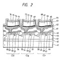
- Fig. 2 is a cross-sectional view of a part of a solid-state image sensor device constituting an embodiment of the photoelectric conversion device.
- a unit cell CLr for obtaining a red signal is composed of 46, 47, 48, 49, 50, 66, 67, 68 and 64; while a unit cell CLg for obtaining a green signal is composed of 51, 52, 53, 54, 55, 70, 71, 72 and 64; and a unit cell CLb for obtaining a blue signal is composed of 56, 57, 58, 59, 60, 74, 75, 76 and 64.
- a p-Si substrate 41 there are shown a p-Si substrate 41; an n+ embedded layer 42; an n ⁇ epitaxial layer 43; an n+ layer 44; and a thick insulating layer 45 formed between adjacent cells, for example by a LOCOS (local oxidation Si) process, and the cells are electrically separated by the layers 44 and 45.
- Polycrystalline Si emitter electrodes 47, 52, 57 are formed respectively corresponding to the cells. Said electrodes may however be replaced by aluminum electrodes, eventually employing TiN as a barrier metal.
- p-base layers 47, 52, 57 formed in respective cells
- n+-emitter layers 48, 53, 58 formed in respective cells
- base electrodes 50, 55, 60 formed in respective cells and maintained in contact with the p-base layers 47, 52, 57 through contact holes 49, 54, 59
- an insulating layer 62 and lower electrodes 66, 70, 74 of photoconductive films 67, 71, 75, electrically connected with the base electrodes 50, 55, 60 at positions 65, 69, 73.
- the step above the insulating layer 62 is reduced by the presence thereof.
- the photoconductive films 67, 71, 75 are composed of i-type amorphous silicon carbide, with respective compositions of i-type a-Si 1-x(0) C x(0) for the film 67, i-type a-Si 1-y(0) C y(0) for the film 71 and i-type a-Si 1-z(0) C z(0) for the film 75, wherein "a-"stands for "amorphous".
- x(0), y(0) and z(0) are so determined that they satisfy a relation: x(0) ⁇ y(0) ⁇ z(0) (1) and that peak spectral sensitivities of about 650 nm, 550 nm and 450 nm are respectively obtained by x(0), y(0) and z(0).
- Blocking layers 68, 72, 76 for the photoconductive films 61, 62, 63 are respectively composed of p-type a-Si l-x(1) C x(1) , p-type a-Si 1-y(1) C y(1) and p-type a-Si 1-z(1) C z(1) , wherein x(1), y(1) and z(1) satisfy following relations: x(0) ⁇ x(1) (2) y(0) ⁇ y(1) (3) z(0) ⁇ z(1) (4). There are also provided a transparent electrode 64 and an insulating layer 63.
- the base electrode 50 and the transparent electrode 64 are at first biased at a resetting potential V RESET . Then the base electrode 50 is disconnected from the reference potential source, thereby maintaining the base layer 47 in a floating state. Subsequently the emitter electrode 46 is connected to a reference potential source of a potential lower than the resetting potential V RESET thereby resetting again the potential of the base layer.
- a negative pulse (amplitude ⁇ ) is supplied to the transparent electrode 64, whereby it assumes a potential V RESET - ⁇ (> 0).
- V RESET - ⁇ (> 0).
- the potential of the base layer 47 is lowered by the capacity C ⁇ between the electrodes 66 and 64 across the photoconductive film 67, and an NPN transistor consisting of the emitter 48, base 47 and embedded collector layer 42 is turned off.
- the amount ⁇ ′ of decline of the potential of the base layer 47 satisfies a relation:
- the potential of the emitter 48 is reset to an extent that the emitter 48 and the base 47 are not biased in the forward direction, and the emitter electrode 46 is connected to a charge readout capacitor, whereby the emitter is maintained in a floating state.
- the transparent electrode 64 is given a positive pulse (amplitude ⁇ ) which elevates, in an inverse fashion to the start of charge accumulation, the potential of the base layer 47 due to the capacity C ⁇ between the electrodes 66 and 64 across the photoconductive film 67, whereby the bipolar transistor consisting of the emitter 48, base 47 and collector 42 is turned on to transfer the potential of the base layer through the emitter 48 to the readout capacitor.
- the present embodiment employing a method of base potential decline in proportion to the amount of incident light, has negative-type characteristics in which the signal read by said readout capacitor is largest in the dark state and decreases with the increase in the amount of incident light.
- the function of the cells for green and blue light is essentially same as that for red light explained above, except that the photoconductive film 71 for green light has a band gap showing a peak spectral sensitivity at ca. 550 nm while the film 75 for blue light has a band gap showing a peak spectral sensitivity at ca. 450 nm, so that they provide signals in respective wavelength regions.
- Fig. 3 is a circuit diagram of the solid-state image sensor device of the first embodiment of the present invention
- Fig. 4 is a timing chart showing the function thereof.
- Fig. 3 shows only three lines respectively for red, green and blue colors, each 3 bits.
- Fig. 3 there are shown: 101, 102, 103: NPN bipolar transistors; 104, 105, 106: capacitances of the photoconductive films; 107, 108, 109: resetting p-channel MOS transistors for maintaining a constant base potential for the NPN transistors; 110, 111, 112: transferring n-channel MOS transistors for transferring the signal charges from the NPN transistors to the capacitances 119, 120, 121; 113, 114, 115: transfer switches to be scanned by a horizontal shift register 140 for successive transfer of the signal charges accumulated in the capacitances 119, 120, 121; 116, 117, 118: resetting n-channel MOS transistors for dissipating the positive holes accumulated in the bases of the NPN transistors and the residual charges of the capacitances of the vertical lines; 130: a resetting switch for resetting a readout line 125; 131: an amplifier; 141: a vertical shift register
- the positive holes accumulated in the bases are dissipated by the combination of two resetting operations, so that output signal can be obtained with extremely low noise level.
- the transparent electrode of the photoconductive film is brought to a potential V RESET - ⁇ at t5, whereby the potential of the bases is lowered by the capacitances 104 - 106 of the photoconductive film.
- the base and emitter of the NPN transistor of each cell are inversely biased to turn off said NPN transistor. If light enters through the transparent electrode in this state, electron-hole pairs are generated in the photoconductive film, and the positive holes move toward the transparent electrode while the electrons move toward the base of the NPN transistor, thereby lowering the potential of the base according to the amount of incident light. (Readout operation)
- V OR is shifted to V RESET and the signal ⁇ T is shifted to the high level at t6, whereby the signals corresponding to the amount of incident light during the accumulation time, or to the base potentials, are transferred, as signal charges, to the capacitances 119 - 121.
- the reset switch 130 is turned on at t8 to reset the line 125, and the transfer switch 113 is turned on at t9 to release the signal charge, accumulated in the capacitance 119, through the amplifier 131. Thereafter the output line 125 is reset again at t10.
- the image information is obtained by repeating the resetting operation, accumulating operation and readout operation explained above, by vertical scanning.
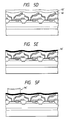
- Ap-Si substrate 41 was surfacially oxidized, then the oxide film was selectively removed in the areas where the embedded collector layers are to be formed, and the n+ embedded layer 42 was formed by diffusion of n-type impurity. Subsequently the n ⁇ -layer 43 of a thickness of 2 - 3 ⁇ m was formed with an impurity concentration of 1014 - 1015 cm ⁇ 3 by epitaxial growth.
- the oxide film and the nitrode film were selectively removed in the areas where the separating areas are to be formed, and As ion injection and thermal oxidation were conducted, thereby forming the separating areas with a bird's beak, composed of the oxide film 45 and the n+ layer 44.
- the impurity of the embodded layer 42 migrate upward whereby the effective thickness of the epitaxial layer of the impurity concentration not exceeding 2 x 1015 cm ⁇ 3 becomes 0.2 - 0.3 ⁇ m, thereby obtaining an inclined collector structure with improved large current characteristics.
- b+ ions were implanted, with a doze of 1 x 1013 cm ⁇ 2 and an accelerating voltage of 20 keV, in the areas where the base areas are to be formed, utilizing a photoresist mask, and the base areas 47, 52, 57 were formed by annealing. Then the oxide film for ion implantation was removed, and an oxide film of a thickness of 3000 ⁇ was formed by CVD. Then As ions were implanted with a doze of 5 x 1014 cm ⁇ 2 and an accelerating voltage of 25 keV, and the emitter layers 48, 53, 58 were prepared by annealing.
- the oxide films were removed in the areas where the contact holes of the emitters are to be formed, then a polycrystalline Si film was formed by CVD and patterned by reactive ion etching to form the emitter electrodes 46, 51, 56 (Fig. 5B). Then the interlayer insulating film 61 was formed by deposition of silicon oxide with CVD, and was removed in the areas for contact with the bases. A Mo film was formed thereon by RF-DC coupled bias sputtering, and was patterned to form the base electrodes 50, 55, 60 (Fig. 5C).
- the n+ polycrystalline silicon film 66′ was formed by CVD (Fig. 5E).
- the photoelectric conversion layer was formed by depositing, in succession, the i-type a-SiC:H film and the p-type a-SiC:H film.
- the film formation was conducted by plasma CVD employing SiH4, H2, C2H2 and B2H6 selectively as the source gasses, with an RF power density of 15 mW/cm2, a pressure of 2 Torr and a substrate temperature of 230°C.
- the photoelectric conversion layer thus formed was patterned to obtain the blue photoelectric conversion area 75′ (Fig. 5F).
- the insulating layer 63 was then formed by depositing silicon oxide by CVD, then was holed for contact with the photoelectric conversion areas, and an ITO film was formed as the transparent electrode.
- the principal part of the solid-state image sensor device as shown in Fig. 2 was completed in this fashion.
- the first embodiment attains high-speed response by high-speed resetting and high-speed readout, since the resetting and the signal readout are conducted by controlling the potential of the base areas serving as the control electrode areas, utilizing the photoelectric conversion layers.
- a solid-state image sensor device constituting a second embodiment of the photoelectric conversion device of the present invention, with reference to Fig. 6, wherein same components as those in Fig. 2 are represented by same numbers or symbols.
- the present embodiment differs from the first embodiment in two aspects.
- the first difference is that the blocking layers 77, 78, 79 are respectively composed of n-type a-Si 1-x(2) C x(2) , n-type a-Si 1-y(2) C y(2) and n-type a-Si 1-z(2) c z(2) , wherein x(2), y(2) and z(2) satisfy: x(0) ⁇ x(2) (6) y(0) ⁇ y(2) (7) z(0) ⁇ z(2) (8).
- the second difference is that, as shown in Fig. 6, polycrystalline Si electrodes 80, 81, 82 are respectively provided for the base layers 47, 52, 57, across gate oxide films.
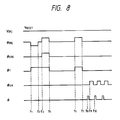
- Fig. 7 is a circuit diagram of the solid-state image sensor device of the second embodiment, and Fig. 8 is a timing chart showing the function thereof.
- the circuit is different from that of the first embodiment, in the presence of capacitances 251, 252, 253 for respective pixels.
- the remaining structure is similar to that of the first embodiment, and will therefore be briefly explained.
- NPN bipolar transistors 201 - 203 there are provided NPN bipolar transistors 201 - 203; capacitances 204 - 206 of the photoelectric conversion films; resetting p-MOS transistors 207 - 209; transferring n-MOS transistors 210 - 213; transfer switches 213 - 215; resetting n-MOS transistors 216 - 218; capacitances 219 - 221 for accumulating signal charges; an output line 225; a reset switch 230 for resetting the output line 225; an amplifier 231; a horizontal shift register 240; a vertical shift register 241; and a scanning driver 242.
- Scanning is made by selecting a horizontal line by the vertical shift register 241 and the driver 242, then effecting the resetting operation, accumulating operation and readout operation, to be described later, on three pixels on said horizontal line, and transferring the signal charges accumulated in the capacitances 219, 220, 221 in succession to the amplifier, by means of the horizontal shift register 240 and the transfer switches 213 - 215.
- the image is read by repeating these operations in succession for different horizontal lines.
- a signal ⁇ BB is shifted down during a period t1 - t2 to turn on the p-MOS transistor, thereby biasing the base electrode 50 and the transparent electrode 64 at the resetting potential V RESET .
- the potential of the transparent electrode 64 may be selected higher than that of the base electrode.
- the p-MOS transistor is turned off to cut off the base electrode 50 from the source of said resetting potential V RESET thereby maintaining the base layer 47 in the floating state, and a positive pulse is supplied to the electrode 80 in a period t3 - t4.
- the potential of the base layer 47 in the floating state is shifted upwards by the capacity C ox between the electrode 80 and the base layer 47, whereby the NPN bipolar transistor consisting of the emitter 48, base 47 and collector 42 is turned on.
- the base layer 47 is reset again by a current in said bipolar transistor.
- a positive pulse ⁇ ers is supplied to turn on the n-MOS transistor, whereby the emitter of the NPN transistor is reset to a potential V EE .
- the potential of the floating base is reset by positive biasing through the capacity C ox .
- the base-emitter junction is deeply forward biased in this fashion to dissipate the photogenerated carriers accumulated in said base, thereby enabling further reduction of the noises.
- a negative pulse is supplied to the electrode 80 at t4.
- Said negative pulse shifts the base potential downwards through said capacity C ox , whereby the transparent electrode assumes a positive potential while the lower electrode 66 connected to the base electrode assumes a negative potential, with respect to the photoconductive film.
- Said positive-negative relationship is inverse to that in the foregoing first embodiment. Consequently, when electron-hole pairs are generated in the photoconductive film 67 by the light entering through the transparent electrode 64, the electrons move toward said transparent electrode 64 and flow out therefrom, while the positive holes move through the base electrode 50 and are accumulated in the base layer 47. Therefore the present embodiment, in which the potential of the base layer 47 is elevated in proportion to the amount of incident light, has positive-type characteristics in contrast to the first embodiment.
- the emitter electrodes 46 are connected to the capacitances 219 - 221 for signal readout, and a positive pulse is supplied to the electrode 80.
- the base potential is elevated to turn on the bipolar transistor consisting of the emitter 48, base 47 and collector 42.
- the signal charges corresponding to the carriers accumulated in the bases are given to the capacitances 219 - 221 connected to the emitters.
- the signals are read as voltages through a deep forward biasing of the base-emitter junction by applying a voltage to the floating base through the capacity C ox .
- the present second embodiment can achieve an improved response by high-speed resetting and can achieve high-speed signal readout since the resetting is conducted utilizing the photoelectric conversion layer.
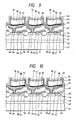
- a solid-state image sensor device constituting a third embodiment of the photoelectric conversion device of the present invention with reference to Fig. 9, which is a cross-sectional view of a photoelectric conversion unit of the present embodiment, wherein same components as those in Fig. 2 are represented by same numbers or symbols.
- the present embodiment is different that shown in Fig.
- a photoconductive film 83 is a superlattice layer consisting of an i-type a-Si layer and a-Si 1-x(3) C x(3)
- a photoconductive film 84 is a superlattice layer consisting of an i-type a-Si layer and a-Si 1-y(3) C y(3)
- a photoconductive film 85 is a superlattice layer consisting of an i-type a-Si layer and a-Si 1-z(3) C z(3) .
- compositions x(3), y(3) and z(3), the thickness Lw of the a-Si layer constituting the well layer of superlattice, and the thickness La of the a-SiC layer constituting the barrier layer are to be so selected that the peak spectral sensitivities are positioned at about 650, 550 and 450 nm respectively for the photoconductive films 83, 84 and 85.
- the use of a superlattice structure in the photoconductive film instead of simple a-SiC layer reduces the resistance of the film, thereby enabling faster resetting of the base layers and the photoconductive films.
- the function of the device of the present embodiment will not be explained as it is similar to that of the first embodiment.
- a solid-state image sensor device constituting a fourth embodiment of the photoelectric conversion device of the present invention, with reference to Fig. 10 which is a cross-sectional view of a photoelectric conversion area of the present embodiment, wherein same components as those in Fig. 2 are represented by same numbers or symbols.
- the present embodiment differs from the first embodiment in that the lower electrodes 86, 87, 88 are respectively composed of n-type a-Si l-x(4) C x(4) , n-type a-Si l-y(4) C y(4) and n-type a-Si l-z(4) C z(4) , wherein compositions x(4), y(4) and z(4) satisfy: x(0) ⁇ x(4) (9) y(0) ⁇ y(4) (10) z(0) ⁇ z(4) (11).
- the contact between the base electrode and the photoconductive film is achieved through an n-type a-SiC film.
- an a-SiC film is employed as a blocking layer between the transparent electrode and the photoconductive film, but there may naturally be employed a transparent Schottky electrode.
- a solid-state image sensor device constituting a fifth embodiment of the photoelectric conversion device of the present invention, with reference to Fig. 11, which is a cross-sectional view of a photoelectric conversion area of the present embodiment, wherein same components as those in Fig. 2 are represented by same numbers or symbols.
- a p-Si substrate 21 there are provided a p-Si substrate 21; a p-well layer 22; a channel stop layer 23; a thick oxide film 24, wherein cells are mutually separated by the combination of the layers 23 and 24; vertical CCD transfer areas 525, 625, 725 respectively for red signal, green signal and blue signal; polycrystalline Si electrodes 527, 627, 727 for transferring the carriers respectively from the photoconductive films 67, 71, 75 to the n+ layers 536, 636, 736; polycrystalline Si electrodes 526, 626, 726 for controlling the transfer from said layers 536, 636, 736 to the vertical CCD areas 525, 625, 725 and the transfer among the vertical CCD areas; and signal readout gates 535, 635, 735 respectively for red, green and blue signals.
- the present embodiment has charge-coupled device (CCD) structures under the photoconductive films.
- CCD charge-coupled device
- the photoelectric conversion area has a structure same as that in the first embodiment, but the structures of the second to fourth embodiment may naturally be employed instead.
- the present embodiment is same in the basic structure as the first embodiment, but differs therefrom only in the structure of the photoelectric conversion layer.
- the lower electrode was composed of n+ polycrystalline silicon, laminated in succession by an i-type a-Si 0.75 C 0.25 :H layer and a p+ a-Si 0.65 C 0.35 :H layer.
- the green color conversion layer was composed of n+ polycrystalline silicon, laminated in succession thereon by an n+ Si:H layer an i-type a-Si:H layer and a p+-type a-Si 0.9 C 0.1 :H layer.
- the red color conversion layer was composed of n+ polycrystalline silicon, laminated in succession thereon by an n+-type a-Si 0.7 Ge 0.3 :H layer, an i-type a-Si 0.7 Ge 0.3 :H layer and a p+-type a-Si:H layer.
- the present embodiment is same in the basic structure as the 6th embodiment, but differs therefrom only in the structure of the photoelectric conversion layer.
- the blue color conversion layer was composed of an n+-type a-Si 0.8 N 0.2 :H layer, an i-type a-Si 0.8 N 0.2 :H layer and a p+-type a-Si 0.7 N 0.3 :H layer.
- the green color conversion layer was composed of an n+-type a-Si:H layer, an i-type a-Si:H layer and a p+-type a-Si 0.9 N 0.1 :H layer.
- the red color conversion layer was same as that in the 6th embodiment.
- the present embodiment is same in basic structure as the foregoing embodiment, but differs therefrom only in the structure of the photoelectric conversion layer. More specifically the film 83 for red color is composed of superlattice layer consisting of an i-type a-Si layer and a-SiGe; the film 84 for green color is composed of an i-type a-Si layer; and the film 85 for blue color is composed of a super lattice layer consisting of an i-type a-Si layer and a-SiC.
- the photoelectric conversion device is integrated on a semiconductor substrate, for example together with a shift register, a driver, photoelectric conversion cells and reference potential sources, and is formed as a chip by sealing for example with transparent resin, with minimum necessary terminal exposed to the outside.
- Such chip can be mounted as an image sensor for example in a video camera, and is suitably connected, through the externally exposed terminals, with a control circuit, input signal lines, output signal lines, driving power sources etc. of the main body. It executes reading of a color image in response to commands supplied from the control circuit of the main body, and sends thus obtained image signals to a signal processing circuit.
- the present invention provides a solid-state color image sensor device which does not require color filters, thereby achieving a fast response, a high sensitivity and a high resolving power.
Landscapes
- Solid State Image Pick-Up Elements (AREA)
- Transforming Light Signals Into Electric Signals (AREA)
Applications Claiming Priority (4)
| Application Number | Priority Date | Filing Date | Title |
|---|---|---|---|
| JP9089/89 | 1989-01-18 | ||
| JP908989 | 1989-01-18 | ||
| JP906967A JPH02275670A (ja) | 1989-01-18 | 1990-01-16 | 光電変換装置および画像読取装置 |
| JP6967/90 | 1990-01-16 |
Publications (2)
| Publication Number | Publication Date |
|---|---|
| EP0379349A2 true EP0379349A2 (fr) | 1990-07-25 |
| EP0379349A3 EP0379349A3 (fr) | 1991-03-20 |
Family
ID=26341185
Family Applications (1)
| Application Number | Title | Priority Date | Filing Date |
|---|---|---|---|
| EP19900300474 Withdrawn EP0379349A3 (fr) | 1989-01-18 | 1990-01-17 | Elément de conversion photoélectrique |
Country Status (1)
| Country | Link |
|---|---|
| EP (1) | EP0379349A3 (fr) |
Cited By (1)
| Publication number | Priority date | Publication date | Assignee | Title |
|---|---|---|---|---|
| CN120151674A (zh) * | 2025-05-15 | 2025-06-13 | 天津希格玛微电子技术有限公司 | 一种高灵敏度像素电路及图像传感器 |
Family Cites Families (4)
| Publication number | Priority date | Publication date | Assignee | Title |
|---|---|---|---|---|
| US3860956A (en) * | 1972-03-17 | 1975-01-14 | Matsushita Electric Industrial Co Ltd | Color target and method of manufacturing same |
| JPS5850030B2 (ja) * | 1979-03-08 | 1983-11-08 | 日本放送協会 | 光電変換装置およびそれを用いた固体撮像板 |
| US4694317A (en) * | 1984-10-22 | 1987-09-15 | Fuji Photo Film Co., Ltd. | Solid state imaging device and process for fabricating the same |
| JPS61193479A (ja) * | 1985-02-22 | 1986-08-27 | Fuji Photo Film Co Ltd | 固体カラ−撮像デバイス |
-
1990
- 1990-01-17 EP EP19900300474 patent/EP0379349A3/fr not_active Withdrawn
Cited By (2)
| Publication number | Priority date | Publication date | Assignee | Title |
|---|---|---|---|---|
| CN120151674A (zh) * | 2025-05-15 | 2025-06-13 | 天津希格玛微电子技术有限公司 | 一种高灵敏度像素电路及图像传感器 |
| CN120151674B (zh) * | 2025-05-15 | 2025-07-29 | 天津希格玛微电子技术有限公司 | 一种高灵敏度像素电路及图像传感器 |
Also Published As
| Publication number | Publication date |
|---|---|
| EP0379349A3 (fr) | 1991-03-20 |
Similar Documents
| Publication | Publication Date | Title |
|---|---|---|
| US5084747A (en) | Photoelectric conversion device having cells of different spectral sensitivities | |
| US12002836B2 (en) | Pixel with strained silicon layer for improving carrier mobility and blue response in imagers | |
| CA1257922A (fr) | Convertisseur photoelectrique | |
| US4862237A (en) | Solid state image sensor | |
| US6180969B1 (en) | CMOS image sensor with equivalent potential diode | |
| US6051447A (en) | Partially pinned photodiode for solid state image sensors | |
| US6943051B2 (en) | Method of fabricating heterojunction photodiodes integrated with CMOS | |
| US5283428A (en) | Photoelectric converting device and information processing apparatus employing the same | |
| US6927089B2 (en) | CMOS imager and method of formation | |
| EP2287917B1 (fr) | Photorecepteur et dispositif de conversion photoélectrique | |
| JPH07115184A (ja) | 積層型固体撮像装置及びその製造方法 | |
| EP0186162B1 (fr) | Capteur d'image à l'état solide | |
| EP0020175B1 (fr) | Dispositif de formation d'image à semiconducteur | |
| JP3315962B2 (ja) | 固体撮像素子、その製造方法及び固体撮像装置 | |
| EP0055114B1 (fr) | Dispositif capteur d'images à semiconducteurs | |
| CA1145835A (fr) | Dispositif photoelectrique, et methode de production connexe | |
| Chikamura et al. | A high-sensitivity solid-state image sensor using a thin-film ZnSe-Zn 1-x Cd x Te heterojunction photosensor | |
| KR100813800B1 (ko) | 암전류 특성과 전하저장능력을 향상시킨 이미지센서 및 그제조방법 | |
| JPH07335936A (ja) | 光電変換装置 | |
| JP3466936B2 (ja) | 固体撮像装置及び固体撮像装置の製造方法 | |
| KR840002282B1 (ko) | 고체 촬상장치 | |
| JPS6051081A (ja) | 半導体撮像装置 |
Legal Events
| Date | Code | Title | Description |
|---|---|---|---|
| PUAI | Public reference made under article 153(3) epc to a published international application that has entered the european phase |
Free format text: ORIGINAL CODE: 0009012 |
|
| AK | Designated contracting states |
Kind code of ref document: A2 Designated state(s): DE ES FR GB NL |
|
| PUAL | Search report despatched |
Free format text: ORIGINAL CODE: 0009013 |
|
| 17P | Request for examination filed |
Effective date: 19901231 |
|
| AK | Designated contracting states |
Kind code of ref document: A3 Designated state(s): DE ES FR GB NL |
|
| 17Q | First examination report despatched |
Effective date: 19940128 |
|
| STAA | Information on the status of an ep patent application or granted ep patent |
Free format text: STATUS: THE APPLICATION IS DEEMED TO BE WITHDRAWN |
|
| 18D | Application deemed to be withdrawn |
Effective date: 19970225 |