EP0379828A2 - Dispositif de traitement par plasma multipolaire à induction de radiofréquence - Google Patents
Dispositif de traitement par plasma multipolaire à induction de radiofréquence Download PDFInfo
- Publication number
- EP0379828A2 EP0379828A2 EP89480185A EP89480185A EP0379828A2 EP 0379828 A2 EP0379828 A2 EP 0379828A2 EP 89480185 A EP89480185 A EP 89480185A EP 89480185 A EP89480185 A EP 89480185A EP 0379828 A2 EP0379828 A2 EP 0379828A2
- Authority
- EP
- European Patent Office
- Prior art keywords
- chamber
- plasma
- work piece
- induction
- accordance
- Prior art date
- Legal status (The legal status is an assumption and is not a legal conclusion. Google has not performed a legal analysis and makes no representation as to the accuracy of the status listed.)
- Granted
Links
Images


Classifications
-
- H—ELECTRICITY
- H01—ELECTRIC ELEMENTS
- H01J—ELECTRIC DISCHARGE TUBES OR DISCHARGE LAMPS
- H01J37/00—Discharge tubes with provision for introducing objects or material to be exposed to the discharge, e.g. for the purpose of examination or processing thereof
- H01J37/32—Gas-filled discharge tubes
- H01J37/32009—Arrangements for generation of plasma specially adapted for examination or treatment of objects, e.g. plasma sources
- H01J37/32082—Radio frequency generated discharge
- H01J37/321—Radio frequency generated discharge the radio frequency energy being inductively coupled to the plasma
-
- H—ELECTRICITY
- H01—ELECTRIC ELEMENTS
- H01J—ELECTRIC DISCHARGE TUBES OR DISCHARGE LAMPS
- H01J37/00—Discharge tubes with provision for introducing objects or material to be exposed to the discharge, e.g. for the purpose of examination or processing thereof
- H01J37/32—Gas-filled discharge tubes
- H01J37/32431—Constructional details of the reactor
- H01J37/32623—Mechanical discharge control means
-
- H—ELECTRICITY
- H01—ELECTRIC ELEMENTS
- H01J—ELECTRIC DISCHARGE TUBES OR DISCHARGE LAMPS
- H01J37/00—Discharge tubes with provision for introducing objects or material to be exposed to the discharge, e.g. for the purpose of examination or processing thereof
- H01J37/32—Gas-filled discharge tubes
- H01J37/32431—Constructional details of the reactor
- H01J37/3266—Magnetic control means
- H01J37/32688—Multi-cusp fields
Definitions
- This invention relates to apparatus for plasma processing of substrates, and more particularly to subtractive (etching) and additive (deposition) processing of electronic circuit chips and packaging materials.
- the problem with capacitive coupling of R.F. energy to a plasma employed for etching or depositing films is that to increase power to the level required to generate the plasma required, the voltage will be so high that the charged particles in the plasma will be accelerated to an excessive level of kinetic energy and will tend to sputter the work piece and to etch or sputter away any masks.
- the effect will be to chamfer the mask opening, i.e. increase the size of openings in masks by etching the edges of the masks.
- the effect also leads to ion damage and loss of selectivity. This is unacceptable as the requirements in the art are to decrease the size of openings as dimensions are decreasing in microelectronics. Instead one would like the flexibility of varying the ion energy according to the desired process.
- U.S. patent 3,705,091 of Jacob for "Gas Discharge Apparatus” shows a cylindrical glass reaction chamber coaxially wound with a helical R.F. coil energized by high frequency (13.5 mHz) R.F. to generate a plasma in a vacuum for etching of a tray of semiconductor slices.
- the system operates in the 1 Torr pressure range and produces mainly reactive radicals.
- the Jacob system does not operate in the desired reactive ion etching, RIE mode of this invention. In the pressure range desired for the present invention of 1 to 50 mTorr, the Jacob system would produce very non-uniform and very slow etching. No means for confining the plasma is shown.
- Desilets et al describes a reactive ion etching tool having a cylindrical reactive ion etching chamber acting as an anode and a plate arrangement acting as a cathode and wherein an R.F. signal applied between cathode and anode acts to produce an active glow region within the chamber with a dark space existing over the internal surfaces thereof.
- a reactive ion etching chamber structure has an internal top surface and sidewall surfaces forming a physically symmetrical arrangement with respect to the cathode plate positioned between the sidewall surfaces below the top surface, the top surface and surfaces being uniform except for gas input and exhaust ports with the gas exhaust ports having an opening dimension less than the thickness of the dark space existing over the internal surface.
- dry processing apparatus for plasma etching or deposition includes a chamber for plasma processing having an external wall for housing a work piece with a surface to be plasma processed in a gas.
- a source of an induction field is located outside the chamber on its opposite side from the work piece.
- a radio frequency (R.F.) induction field applied to the chamber generates a plasma in the gas.
- the plasma is confined within the external wall in the chamber by magnetic dipoles providing a surface magnetic field for confining the plasma.
- the surface magnetic field is confined to the space adjacent to the external wall.
- An R.F. generator provides an R.F. generated bias to the work piece.
- the chamber is lined with a material inert to a plasma or noncontaminating to the work piece, and the induction source in the form of an involut or spiral induction coil is located on the exterior of the liner material on the opposite side of the chamber from the work piece. Delivery of and distribution of the gas to the chamber is uniform about the periphery of the top cover because a manifold is located about the periphery of the chamber.
- An orifice for controlling the gas pressure of the gas being admitted to the chamber is formed by the surface of the chamber and the manifold admits gas from the manifold into the chamber at a uniform pressure about the periphery of the cover of the chamber.
- a surface magnetic field is positioned adjacent to the induction coil to confine the field at the top of the chamber. It is further preferred that a capacitive or inductive reactance be connected in series with the induction coil to adjust the R.F. generated bias.
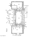
- FIG. 1 shows apparatus 9 which includes an evacuated chamber 10 containing a semiconductor wafer 11 that comprises a work piece to be treated with a plasma process.
- a gas is admitted to chamber 10 from annular manifold 14 via annular orifice 15. The gas is used to form a plasma for processing of wafer 11 by etching or deposition.
- a liner 16 forming a cylindrical outer wall contains the gas which is to be energized to form a plasma.
- liner 16 is composed of quartz or another material which is nearly, i.e. substantially, inert or noncontaminating to the plasma to be contained in plasma processing chamber 10.
- the cover 17 of the chamber 10 is composed of quartz also.
- the chamber 10 is surrounded by quartz lined liner 16 and cover 17 on the sides and the top with the wafer 11 on the bottom.
- the wafer 11 is supported on metallic base 23, but is insulated therefrom by an insulating coating on the upper surface of base 23.
- a flat insulating ring 40 is provided on top of base 23 at the periphery of the wafer 11 and with an indentation 32 for supporting the edges of wafer 11. Ring 40 separates the plasma from the surfaces below, and it is shown shaped with indentation 32 to retain the wafer 11 in a central position at the base of chamber 10.
- the gas is admitted to the chamber 10 from gas input port 12 through line 13 to annular manifold 14 formed by annular base 27 and the cover 17.
- the manifold 14 is about 0.275 inches deep.
- the manifold 14 is connected to chamber 10 through a circumferential, narrow annular orifice 15 of about 0.005 inches which maintains sufficient pressure of the gas in manifold 14 that the gas is distributed at a relatively uniform pressure about the entire circumference of the top of chamber 10.
- the gas in manifold 14 passes through orifice 15 between the top of the lip of annular base 27 and the lower surface of cover 17 in substantially equal quantities per unit time all about the circumferential area, i.e. the periphery, at the top of chamber 10 so that the plasma will be more highly uniform within the chamber 10.
- the pressure of the gas in chamber 10 is at a low pressure of about 1-5 mTorr.
- the gas to be exhausted from chamber 10 passes through annular orifice 18 at the base of the liner 16 or between magnets 21 into exhaust vacuum pumping manifold 19 and out through port 89, which is connected to vacuum pumps (not shown for convenience of illustration.)
- Apparatus to provide magnetic confinement of the plasma is employed in the form of multiple-magnetic-dipoles (multipoles) 21 with vertical axes as shown in FIGS. 1, 2 and 3.
- the multipoles 21 have their fields directed at right angles towards the vertical axis of the cylindrical chamber 10.
- Multipoles 21 are arranged about the periphery of liner 16 in the classic magnetic confinement cylindrical arrangement.
- the multipoles have their magnetic field directed inwardly as indicated by the plan view in FIG. 2. With this arrangement the alternating of the north and south poles (of multipoles 21) directed inwardly, looking down as in FIG.
- Source 30 is connected by line 38 to the outer end of coil 22 at terminal 47.
- the other end of source 30 is also connected to ground completing the circuit.
- the inner end of spiral coil 22 is connected at terminal 28 by line 46 through switch 48 and line 39 to a bond 29 on the grounded wall 31 of apparatus 9 which is at electrical ground.
- magnetic multipole confinement by magnets 32 located above cover 17 on its surface can be added adjacent to coil 22 to reduce the plasma loss to cover 17.
- Reactance 50 can be a variable or fixed reactance which is capacitive or inductive, as desired, to adjust the R.F. bias on the plasma.
- the connection of reactance 50 in series with coil 22, between terminal 28 and ground connection 29, is employed for the case where one is using the R.F. coil 22 alone, i.e. not using R.F. bias from source 24.
- Reactance 50 is useful in a case in which it is desired to use R.F. induction without the R.F. bias from source 24. In this case one can vary the ion energy over a somewhat smaller range 10eV to 80 eV.
- one varies the impedance to ground (from the center of the coil 22, bypassing line 39 when switch 48 is opened to close the circuit to ground through reactance 50 and lines 49, 51 and 39 as well as bond 29).
- This allows one to go from the smallest amount of capacitive coupling (equivalent to middle turn 34 being at R.F. ground potential) with a value of capacitive impedance equal to one half of the coils inductive impedance to somewhat more capacitive coupling for reactance 50 being inductive.
- coil 22 includes a spiral with terminals, tapped holes comprising terminals 28 and 47 respectively for joining lines 28 and 38 to coil 22.
- Coil 22 is shown having three turns with the second (middle) turn 34 from transition 33 to transition 35 being substantially wider to enhance the inductive qualities of the coil 22.
- Both the outer turn 36 and the inner turn 37 are of about the same width.
- the advantage of this design is that the plasma is more uniform beneath the second (middle) turn 34 than it would be with a coil with a single width. In general this principle applies regardless of how many turns are involved. What is involved with the variation in width (i.e. cross-sectional area) is that the inductances of the three turns are rebalanced.
- the R.F. energy from the coil 22 ionizes the gas in chamber 10 into a sustained plasma for additive or subtractive processing of the wafer 11.
- the wafer 11 is supported on metallic base 23.
- Metallic base 23 cools wafer 11 with electrostatic clamping and backside cooling not shown for convenience of illustration, but as is well understood by those skilled in the art.
- Base 23 is connected to an R.F. biasing source 24 at a frequency above about 13 MHz, preferably at 40 MHz which sets up an R.F. bias between the wafer 11 and the plasma, leading to a D.C. bias on the wafer 11.
- the use of different frequencies reduces coupling between the two power supplies.
- the high frequency R.F. bias gives a more monotonic distribution of ion energy, so there is improved control of ion energy for better selectivity of the rate of etching.
- This R.F. bias provides ion energy control of the ions from the plasma as the R.F. level of the base 23 is varied by R.F. source 24.
- a dark space exists upon the upper surface of the wafer 11.
- the use of R.F. coil 22 instead of a capacitively coupled R.F. electrode to generate the plasma affords the advantage of reducing and controlling the kinetic energy of the ions striking the walls of liner 16 and wafer 11, thereby reducing the damage that can be done by ions and electrons at the high energy levels required for plasma processing contemplated for use with this apparatus. This also gives the flexibility of adjusting the ion energy according to process needs.
- the other dotted curve is for a system in which the plasma is formed by an R.F. diode, i.e. capacitively coupled R.F.. It can be seen that at higher power levels, the R.F. induction produces far higher ion current at a given power level plus a linear rate of increase which are both preferred characteristics. Ion current does not saturate as power increases, so very high plasma densities can be achieved at low ion kinetic energies.
- This system can replace wet HF solutions for etching of thin layers.
Landscapes
- Physics & Mathematics (AREA)
- Engineering & Computer Science (AREA)
- Plasma & Fusion (AREA)
- Chemical & Material Sciences (AREA)
- Analytical Chemistry (AREA)
- Drying Of Semiconductors (AREA)
- ing And Chemical Polishing (AREA)
- Plasma Technology (AREA)
- Electrodes Of Semiconductors (AREA)
Applications Claiming Priority (2)
| Application Number | Priority Date | Filing Date | Title |
|---|---|---|---|
| US30193389A | 1989-01-25 | 1989-01-25 | |
| US301933 | 1989-01-25 |
Publications (3)
| Publication Number | Publication Date |
|---|---|
| EP0379828A2 true EP0379828A2 (fr) | 1990-08-01 |
| EP0379828A3 EP0379828A3 (fr) | 1991-01-09 |
| EP0379828B1 EP0379828B1 (fr) | 1995-09-27 |
Family
ID=23165518
Family Applications (1)
| Application Number | Title | Priority Date | Filing Date |
|---|---|---|---|
| EP19890480185 Expired - Lifetime EP0379828B1 (fr) | 1989-01-25 | 1989-12-19 | Dispositif de traitement par plasma multipolaire à induction de radiofréquence |
Country Status (3)
| Country | Link |
|---|---|
| EP (1) | EP0379828B1 (fr) |
| JP (1) | JPH0770532B2 (fr) |
| DE (1) | DE68924413T2 (fr) |
Cited By (51)
| Publication number | Priority date | Publication date | Assignee | Title |
|---|---|---|---|---|
| EP0413282A3 (en) * | 1989-08-14 | 1991-07-24 | Lam Research Corporation | Method and apparatus for producing magnetically-coupled planar plasma |
| US5241245A (en) * | 1992-05-06 | 1993-08-31 | International Business Machines Corporation | Optimized helical resonator for plasma processing |
| US5280154A (en) * | 1992-01-30 | 1994-01-18 | International Business Machines Corporation | Radio frequency induction plasma processing system utilizing a uniform field coil |
| WO1994006263A1 (fr) * | 1992-09-01 | 1994-03-17 | The University Of North Carolina At Chapel Hill | Plasma a couplage inductif regule par champ magnetique a haute pression |
| EP0633713A1 (fr) * | 1993-07-05 | 1995-01-11 | Alcatel Cit | Réacteur à plasma pour un procédé de dépôt ou de gravure |
| US5433812A (en) * | 1993-01-19 | 1995-07-18 | International Business Machines Corporation | Apparatus for enhanced inductive coupling to plasmas with reduced sputter contamination |
| EP0688037A1 (fr) * | 1994-06-14 | 1995-12-20 | Sumitomo Metal Industries, Ltd. | Système de traitement par plasma micro-ondes |
| US5518547A (en) * | 1993-12-23 | 1996-05-21 | International Business Machines Corporation | Method and apparatus for reducing particulates in a plasma tool through steady state flows |
| US5521351A (en) * | 1994-08-30 | 1996-05-28 | Wisconsin Alumni Research Foundation | Method and apparatus for plasma surface treatment of the interior of hollow forms |
| US5522934A (en) * | 1994-04-26 | 1996-06-04 | Tokyo Electron Limited | Plasma processing apparatus using vertical gas inlets one on top of another |
| US5525159A (en) * | 1993-12-17 | 1996-06-11 | Tokyo Electron Limited | Plasma process apparatus |
| US5529657A (en) * | 1993-10-04 | 1996-06-25 | Tokyo Electron Limited | Plasma processing apparatus |
| US5540800A (en) * | 1994-06-23 | 1996-07-30 | Applied Materials, Inc. | Inductively coupled high density plasma reactor for plasma assisted materials processing |
| US5540824A (en) * | 1994-07-18 | 1996-07-30 | Applied Materials | Plasma reactor with multi-section RF coil and isolated conducting lid |
| US5565114A (en) * | 1993-03-04 | 1996-10-15 | Tokyo Electron Limited | Method and device for detecting the end point of plasma process |
| US5587038A (en) * | 1994-06-16 | 1996-12-24 | Princeton University | Apparatus and process for producing high density axially extending plasmas |
| US5614055A (en) * | 1993-08-27 | 1997-03-25 | Applied Materials, Inc. | High density plasma CVD and etching reactor |
| US5653811A (en) * | 1995-07-19 | 1997-08-05 | Chan; Chung | System for the plasma treatment of large area substrates |
| DE19606375A1 (de) * | 1996-02-21 | 1997-08-28 | Balzers Prozes Systeme Gmbh | Plasmaquelle mit eingekoppelten Whistler- oder Helikonwellen |
| US5683537A (en) * | 1993-10-04 | 1997-11-04 | Tokyo Electron Limited | Plasma processing apparatus |
| US5688357A (en) * | 1995-02-15 | 1997-11-18 | Applied Materials, Inc. | Automatic frequency tuning of an RF power source of an inductively coupled plasma reactor |
| US5739051A (en) * | 1993-03-04 | 1998-04-14 | Tokyo Electron Limited | Method and device for detecting the end point of plasma process |
| US5753044A (en) * | 1995-02-15 | 1998-05-19 | Applied Materials, Inc. | RF plasma reactor with hybrid conductor and multi-radius dome ceiling |
| US5783492A (en) * | 1994-03-04 | 1998-07-21 | Tokyo Electron Limited | Plasma processing method, plasma processing apparatus, and plasma generating apparatus |
| US5851294A (en) * | 1995-10-23 | 1998-12-22 | Watkins-Johnson Company | Gas injection system for semiconductor processing |
| US5938883A (en) * | 1993-01-12 | 1999-08-17 | Tokyo Electron Limited | Plasma processing apparatus |
| US5942855A (en) * | 1996-08-28 | 1999-08-24 | Northeastern University | Monolithic miniaturized inductively coupled plasma source |
| US5951773A (en) * | 1996-03-18 | 1999-09-14 | Hyundai Electronics Industries Co., Ltd. | Inductively coupled plasma chemical vapor deposition apparatus |
| US5982100A (en) * | 1997-07-28 | 1999-11-09 | Pars, Inc. | Inductively coupled plasma reactor |
| US5994207A (en) * | 1997-05-12 | 1999-11-30 | Silicon Genesis Corporation | Controlled cleavage process using pressurized fluid |
| US6027988A (en) * | 1997-05-28 | 2000-02-22 | The Regents Of The University Of California | Method of separating films from bulk substrates by plasma immersion ion implantation |
| US6051073A (en) * | 1998-02-11 | 2000-04-18 | Silicon Genesis Corporation | Perforated shield for plasma immersion ion implantation |
| US6103599A (en) * | 1997-07-25 | 2000-08-15 | Silicon Genesis Corporation | Planarizing technique for multilayered substrates |
| US6136140A (en) * | 1993-01-12 | 2000-10-24 | Tokyo Electron Limited | Plasma processing apparatus |
| US6214162B1 (en) | 1996-09-27 | 2001-04-10 | Tokyo Electron Limited | Plasma processing apparatus |
| US6213050B1 (en) | 1998-12-01 | 2001-04-10 | Silicon Genesis Corporation | Enhanced plasma mode and computer system for plasma immersion ion implantation |
| US6228176B1 (en) | 1998-02-11 | 2001-05-08 | Silicon Genesis Corporation | Contoured platen design for plasma immerson ion implantation |
| US6248250B1 (en) | 1995-02-15 | 2001-06-19 | Applied Materials Inc. | RF plasma reactor with hybrid conductor and multi-radius dome ceiling |
| US6270617B1 (en) | 1995-02-15 | 2001-08-07 | Applied Materials, Inc. | RF plasma reactor with hybrid conductor and multi-radius dome ceiling |
| US6291793B1 (en) | 1994-10-31 | 2001-09-18 | Appplied Materials, Inc. | Inductively coupled plasma reactor with symmetrical parallel multiple coils having a common RF terminal |
| US6335293B1 (en) | 1998-07-13 | 2002-01-01 | Mattson Technology, Inc. | Systems and methods for two-sided etch of a semiconductor substrate |
| US6369348B2 (en) | 1997-06-30 | 2002-04-09 | Applied Materials, Inc | Plasma reactor with coil antenna of plural helical conductors with equally spaced ends |
| US6465051B1 (en) | 1994-04-28 | 2002-10-15 | Applied Materials, Inc. | Method of operating high density plasma CVD reactor with combined inductive and capacitive coupling |
| US6890838B2 (en) | 1997-07-18 | 2005-05-10 | Silicon Genesis Corporation | Gettering technique for wafers made using a controlled cleaving process |
| WO2005057607A3 (fr) * | 2003-12-13 | 2005-11-17 | Roth & Rau Ag | Source plasma destinee a la production d'un plasma de couplage inductif |
| US7056808B2 (en) | 1999-08-10 | 2006-06-06 | Silicon Genesis Corporation | Cleaving process to fabricate multilayered substrates using low implantation doses |
| USRE40963E1 (en) * | 1993-01-12 | 2009-11-10 | Tokyo Electron Limited | Method for plasma processing by shaping an induced electric field |
| US8993410B2 (en) | 2006-09-08 | 2015-03-31 | Silicon Genesis Corporation | Substrate cleaving under controlled stress conditions |
| CN108271309A (zh) * | 2016-12-30 | 2018-07-10 | 中微半导体设备(上海)有限公司 | 一种电感耦合等离子处理装置 |
| US11444221B2 (en) | 2008-05-07 | 2022-09-13 | Silicon Genesis Corporation | Layer transfer of films utilizing controlled shear region |
| CN121709505A (zh) * | 2026-02-13 | 2026-03-20 | 上海邦芯半导体科技有限公司 | 一种反应腔室及晶圆处理设备 |
Families Citing this family (10)
| Publication number | Priority date | Publication date | Assignee | Title |
|---|---|---|---|---|
| CA2207154A1 (fr) * | 1996-06-10 | 1997-12-10 | Lam Research Corporation | Une source inductivement couplee pour deriver le flux de plasma de facon essentiellement uniforme |
| US5993678A (en) * | 1996-07-31 | 1999-11-30 | Toyo Technologies Inc. | Device and method for processing a plasma to alter the surface of a substrate |
| JP3483725B2 (ja) * | 1997-04-02 | 2004-01-06 | 株式会社日立製作所 | プラズマ処理装置及び処理方法 |
| US6033974A (en) | 1997-05-12 | 2000-03-07 | Silicon Genesis Corporation | Method for controlled cleaving process |
| JP2000235900A (ja) * | 1999-02-15 | 2000-08-29 | Tokyo Electron Ltd | プラズマ処理装置 |
| US6263941B1 (en) | 1999-08-10 | 2001-07-24 | Silicon Genesis Corporation | Nozzle for cleaving substrates |
| US6221740B1 (en) | 1999-08-10 | 2001-04-24 | Silicon Genesis Corporation | Substrate cleaving tool and method |
| JP3787079B2 (ja) | 2001-09-11 | 2006-06-21 | 株式会社日立製作所 | プラズマ処理装置 |
| US7464662B2 (en) * | 2004-01-28 | 2008-12-16 | Tokyo Electron Limited | Compact, distributed inductive element for large scale inductively-coupled plasma sources |
| JP4657620B2 (ja) | 2004-04-13 | 2011-03-23 | 株式会社日立ハイテクノロジーズ | プラズマ処理装置 |
Family Cites Families (9)
| Publication number | Priority date | Publication date | Assignee | Title |
|---|---|---|---|---|
| JPS6058794B2 (ja) * | 1981-06-10 | 1985-12-21 | 日本電子株式会社 | プラズマ加工装置 |
| US4431898A (en) * | 1981-09-01 | 1984-02-14 | The Perkin-Elmer Corporation | Inductively coupled discharge for plasma etching and resist stripping |
| FR2538987A1 (fr) * | 1983-01-05 | 1984-07-06 | Commissariat Energie Atomique | Enceinte pour le traitement et notamment la gravure de substrats par la methode du plasma reactif |
| US4483737A (en) * | 1983-01-31 | 1984-11-20 | University Of Cincinnati | Method and apparatus for plasma etching a substrate |
| JPH0740468B2 (ja) * | 1984-12-11 | 1995-05-01 | 株式会社日立製作所 | 高周波プラズマ発生装置 |
| EP0203560A1 (fr) * | 1985-05-31 | 1986-12-03 | Tegal Corporation | Gravure de tranchées à l'aide de plasma |
| GB8622820D0 (en) * | 1986-09-23 | 1986-10-29 | Nordiko Ltd | Electrode assembly & apparatus |
| GB8629634D0 (en) * | 1986-12-11 | 1987-01-21 | Dobson C D | Reactive ion & sputter etching |
| EP0284867A2 (fr) * | 1987-04-03 | 1988-10-05 | Tegal Corporation | Appareil de gravure sèche utilisant un confinement du plasma par champ magnétique de surface |
-
1989
- 1989-12-19 EP EP19890480185 patent/EP0379828B1/fr not_active Expired - Lifetime
- 1989-12-19 DE DE1989624413 patent/DE68924413T2/de not_active Expired - Lifetime
- 1989-12-28 JP JP1338900A patent/JPH0770532B2/ja not_active Expired - Lifetime
Cited By (72)
| Publication number | Priority date | Publication date | Assignee | Title |
|---|---|---|---|---|
| EP0413282A3 (en) * | 1989-08-14 | 1991-07-24 | Lam Research Corporation | Method and apparatus for producing magnetically-coupled planar plasma |
| US5280154A (en) * | 1992-01-30 | 1994-01-18 | International Business Machines Corporation | Radio frequency induction plasma processing system utilizing a uniform field coil |
| US5241245A (en) * | 1992-05-06 | 1993-08-31 | International Business Machines Corporation | Optimized helical resonator for plasma processing |
| WO1994006263A1 (fr) * | 1992-09-01 | 1994-03-17 | The University Of North Carolina At Chapel Hill | Plasma a couplage inductif regule par champ magnetique a haute pression |
| US5648701A (en) * | 1992-09-01 | 1997-07-15 | The University Of North Carolina At Chapel Hill | Electrode designs for high pressure magnetically assisted inductively coupled plasmas |
| US5938883A (en) * | 1993-01-12 | 1999-08-17 | Tokyo Electron Limited | Plasma processing apparatus |
| US6265031B1 (en) | 1993-01-12 | 2001-07-24 | Tokyo Electron Limited | Method for plasma processing by shaping an induced electric field |
| US6136140A (en) * | 1993-01-12 | 2000-10-24 | Tokyo Electron Limited | Plasma processing apparatus |
| US6136139A (en) * | 1993-01-12 | 2000-10-24 | Tokyo Electron Limited | Plasma processing apparatus |
| USRE40963E1 (en) * | 1993-01-12 | 2009-11-10 | Tokyo Electron Limited | Method for plasma processing by shaping an induced electric field |
| US5433812A (en) * | 1993-01-19 | 1995-07-18 | International Business Machines Corporation | Apparatus for enhanced inductive coupling to plasmas with reduced sputter contamination |
| US5622635A (en) * | 1993-01-19 | 1997-04-22 | International Business Machines Corporation | Method for enhanced inductive coupling to plasmas with reduced sputter contamination |
| US5565114A (en) * | 1993-03-04 | 1996-10-15 | Tokyo Electron Limited | Method and device for detecting the end point of plasma process |
| US5739051A (en) * | 1993-03-04 | 1998-04-14 | Tokyo Electron Limited | Method and device for detecting the end point of plasma process |
| FR2707449A1 (fr) * | 1993-07-05 | 1995-01-13 | Cit Alcatel | Réacteur à plasma pour un procédé de dépôt ou de gravure. |
| EP0633713A1 (fr) * | 1993-07-05 | 1995-01-11 | Alcatel Cit | Réacteur à plasma pour un procédé de dépôt ou de gravure |
| US5614055A (en) * | 1993-08-27 | 1997-03-25 | Applied Materials, Inc. | High density plasma CVD and etching reactor |
| US5529657A (en) * | 1993-10-04 | 1996-06-25 | Tokyo Electron Limited | Plasma processing apparatus |
| US5683537A (en) * | 1993-10-04 | 1997-11-04 | Tokyo Electron Limited | Plasma processing apparatus |
| US5525159A (en) * | 1993-12-17 | 1996-06-11 | Tokyo Electron Limited | Plasma process apparatus |
| US5518547A (en) * | 1993-12-23 | 1996-05-21 | International Business Machines Corporation | Method and apparatus for reducing particulates in a plasma tool through steady state flows |
| US5543184A (en) * | 1993-12-23 | 1996-08-06 | International Business Machines Corporation | Method of reducing particulates in a plasma tool through steady state flows |
| US5783492A (en) * | 1994-03-04 | 1998-07-21 | Tokyo Electron Limited | Plasma processing method, plasma processing apparatus, and plasma generating apparatus |
| US5522934A (en) * | 1994-04-26 | 1996-06-04 | Tokyo Electron Limited | Plasma processing apparatus using vertical gas inlets one on top of another |
| US6465051B1 (en) | 1994-04-28 | 2002-10-15 | Applied Materials, Inc. | Method of operating high density plasma CVD reactor with combined inductive and capacitive coupling |
| EP0688037A1 (fr) * | 1994-06-14 | 1995-12-20 | Sumitomo Metal Industries, Ltd. | Système de traitement par plasma micro-ondes |
| US5529632A (en) * | 1994-06-14 | 1996-06-25 | Sumitomo Metal Industries, Ltd. | Microwave plasma processing system |
| US5587038A (en) * | 1994-06-16 | 1996-12-24 | Princeton University | Apparatus and process for producing high density axially extending plasmas |
| US5540800A (en) * | 1994-06-23 | 1996-07-30 | Applied Materials, Inc. | Inductively coupled high density plasma reactor for plasma assisted materials processing |
| US5540824A (en) * | 1994-07-18 | 1996-07-30 | Applied Materials | Plasma reactor with multi-section RF coil and isolated conducting lid |
| US5521351A (en) * | 1994-08-30 | 1996-05-28 | Wisconsin Alumni Research Foundation | Method and apparatus for plasma surface treatment of the interior of hollow forms |
| US6291793B1 (en) | 1994-10-31 | 2001-09-18 | Appplied Materials, Inc. | Inductively coupled plasma reactor with symmetrical parallel multiple coils having a common RF terminal |
| US6297468B1 (en) | 1994-10-31 | 2001-10-02 | Applied Materials, Inc. | Inductively coupled plasma reactor with symmetrical parallel multiple coils having a common RF terminal |
| US5688357A (en) * | 1995-02-15 | 1997-11-18 | Applied Materials, Inc. | Automatic frequency tuning of an RF power source of an inductively coupled plasma reactor |
| US5753044A (en) * | 1995-02-15 | 1998-05-19 | Applied Materials, Inc. | RF plasma reactor with hybrid conductor and multi-radius dome ceiling |
| US6270617B1 (en) | 1995-02-15 | 2001-08-07 | Applied Materials, Inc. | RF plasma reactor with hybrid conductor and multi-radius dome ceiling |
| US6475335B1 (en) | 1995-02-15 | 2002-11-05 | Applied Materials, Inc. | RF plasma reactor with hybrid conductor and multi-radius dome ceiling |
| US6248250B1 (en) | 1995-02-15 | 2001-06-19 | Applied Materials Inc. | RF plasma reactor with hybrid conductor and multi-radius dome ceiling |
| US5653811A (en) * | 1995-07-19 | 1997-08-05 | Chan; Chung | System for the plasma treatment of large area substrates |
| US6338313B1 (en) | 1995-07-19 | 2002-01-15 | Silison Genesis Corporation | System for the plasma treatment of large area substrates |
| US5851294A (en) * | 1995-10-23 | 1998-12-22 | Watkins-Johnson Company | Gas injection system for semiconductor processing |
| DE19606375A1 (de) * | 1996-02-21 | 1997-08-28 | Balzers Prozes Systeme Gmbh | Plasmaquelle mit eingekoppelten Whistler- oder Helikonwellen |
| US6380612B1 (en) | 1996-03-18 | 2002-04-30 | Hyundai Display Technology, Inc. | Thin film formed by inductively coupled plasma |
| US6093660A (en) * | 1996-03-18 | 2000-07-25 | Hyundai Electronics Industries Co., Ltd. | Inductively coupled plasma chemical vapor deposition technology |
| US5951773A (en) * | 1996-03-18 | 1999-09-14 | Hyundai Electronics Industries Co., Ltd. | Inductively coupled plasma chemical vapor deposition apparatus |
| US5942855A (en) * | 1996-08-28 | 1999-08-24 | Northeastern University | Monolithic miniaturized inductively coupled plasma source |
| US6214162B1 (en) | 1996-09-27 | 2001-04-10 | Tokyo Electron Limited | Plasma processing apparatus |
| US5994207A (en) * | 1997-05-12 | 1999-11-30 | Silicon Genesis Corporation | Controlled cleavage process using pressurized fluid |
| US6013563A (en) * | 1997-05-12 | 2000-01-11 | Silicon Genesis Corporation | Controlled cleaning process |
| US6027988A (en) * | 1997-05-28 | 2000-02-22 | The Regents Of The University Of California | Method of separating films from bulk substrates by plasma immersion ion implantation |
| US6369348B2 (en) | 1997-06-30 | 2002-04-09 | Applied Materials, Inc | Plasma reactor with coil antenna of plural helical conductors with equally spaced ends |
| US6369349B2 (en) | 1997-06-30 | 2002-04-09 | Applied Materials, Inc. | Plasma reactor with coil antenna of interleaved conductors |
| US6373022B2 (en) | 1997-06-30 | 2002-04-16 | Applied Materials, Inc. | Plasma reactor with antenna of coil conductors of concentric helices offset along the axis of symmetry |
| US6504126B2 (en) | 1997-06-30 | 2003-01-07 | Applied Materials, Inc. | Plasma reactor with coil antenna of concentrically spiral conductors with ends in common regions |
| US6890838B2 (en) | 1997-07-18 | 2005-05-10 | Silicon Genesis Corporation | Gettering technique for wafers made using a controlled cleaving process |
| US6103599A (en) * | 1997-07-25 | 2000-08-15 | Silicon Genesis Corporation | Planarizing technique for multilayered substrates |
| US5982100A (en) * | 1997-07-28 | 1999-11-09 | Pars, Inc. | Inductively coupled plasma reactor |
| US6228176B1 (en) | 1998-02-11 | 2001-05-08 | Silicon Genesis Corporation | Contoured platen design for plasma immerson ion implantation |
| US6051073A (en) * | 1998-02-11 | 2000-04-18 | Silicon Genesis Corporation | Perforated shield for plasma immersion ion implantation |
| US6335293B1 (en) | 1998-07-13 | 2002-01-01 | Mattson Technology, Inc. | Systems and methods for two-sided etch of a semiconductor substrate |
| US6624082B2 (en) | 1998-07-13 | 2003-09-23 | Mattson Technology, Inc. | Systems and methods for two-sided etch of a semiconductor substrate |
| US6213050B1 (en) | 1998-12-01 | 2001-04-10 | Silicon Genesis Corporation | Enhanced plasma mode and computer system for plasma immersion ion implantation |
| US7056808B2 (en) | 1999-08-10 | 2006-06-06 | Silicon Genesis Corporation | Cleaving process to fabricate multilayered substrates using low implantation doses |
| WO2005057607A3 (fr) * | 2003-12-13 | 2005-11-17 | Roth & Rau Ag | Source plasma destinee a la production d'un plasma de couplage inductif |
| US8993410B2 (en) | 2006-09-08 | 2015-03-31 | Silicon Genesis Corporation | Substrate cleaving under controlled stress conditions |
| US9356181B2 (en) | 2006-09-08 | 2016-05-31 | Silicon Genesis Corporation | Substrate cleaving under controlled stress conditions |
| US9640711B2 (en) | 2006-09-08 | 2017-05-02 | Silicon Genesis Corporation | Substrate cleaving under controlled stress conditions |
| US11444221B2 (en) | 2008-05-07 | 2022-09-13 | Silicon Genesis Corporation | Layer transfer of films utilizing controlled shear region |
| CN108271309A (zh) * | 2016-12-30 | 2018-07-10 | 中微半导体设备(上海)有限公司 | 一种电感耦合等离子处理装置 |
| CN108271309B (zh) * | 2016-12-30 | 2020-05-01 | 中微半导体设备(上海)股份有限公司 | 一种电感耦合等离子处理装置 |
| CN121709505A (zh) * | 2026-02-13 | 2026-03-20 | 上海邦芯半导体科技有限公司 | 一种反应腔室及晶圆处理设备 |
| CN121709505B (zh) * | 2026-02-13 | 2026-04-14 | 上海邦芯半导体科技有限公司 | 一种反应腔室及晶圆处理设备 |
Also Published As
| Publication number | Publication date |
|---|---|
| EP0379828B1 (fr) | 1995-09-27 |
| DE68924413D1 (de) | 1995-11-02 |
| JPH02235332A (ja) | 1990-09-18 |
| EP0379828A3 (fr) | 1991-01-09 |
| JPH0770532B2 (ja) | 1995-07-31 |
| DE68924413T2 (de) | 1996-05-02 |
Similar Documents
| Publication | Publication Date | Title |
|---|---|---|
| US5304279A (en) | Radio frequency induction/multipole plasma processing tool | |
| EP0379828B1 (fr) | Dispositif de traitement par plasma multipolaire à induction de radiofréquence | |
| EP0271341B1 (fr) | Procédé et dispositif d'attaque par ions | |
| US6211622B1 (en) | Plasma processing equipment | |
| EP0510401B1 (fr) | Dispositif pour traitement par plasma | |
| KR100319664B1 (ko) | 플라즈마처리장치 | |
| US7863582B2 (en) | Ion-beam source | |
| EP0640244B1 (fr) | Appareil de traitement au plasma et procede dans lequel un champ electrique uniforme est induit par une fenetre dielectrique | |
| US6446572B1 (en) | Embedded plasma source for plasma density improvement | |
| EP0396398B1 (fr) | Dispositif de décapage à plasma avec champs magnétiques de surface | |
| US9564297B2 (en) | Electron beam plasma source with remote radical source | |
| US5580420A (en) | Plasma generating method and apparatus and plasma processing method and apparatus | |
| US6333601B1 (en) | Planar gas introducing unit of a CCP reactor | |
| US20030150562A1 (en) | Apparatus and method to control the uniformity of plasma by reducing radial loss | |
| US20010017109A1 (en) | Enhanced plasma mode and system for plasma immersion ion implantation | |
| US6167835B1 (en) | Two chamber plasma processing apparatus | |
| JPH06267903A (ja) | プラズマ装置 | |
| US7060931B2 (en) | Neutral beam source having electromagnet used for etching semiconductor device | |
| US6835279B2 (en) | Plasma generation apparatus | |
| JP3294839B2 (ja) | プラズマ処理方法 | |
| JP2000156374A (ja) | スパッタ処理応用のプラズマ処理装置 | |
| JPH01302645A (ja) | 放電装置 | |
| KR100501823B1 (ko) | 플라즈마 발생 방법 및 그 장치 | |
| US6432730B2 (en) | Plasma processing method and apparatus | |
| KR100501821B1 (ko) | 플라즈마 발생 방법 및 그 장치 |
Legal Events
| Date | Code | Title | Description |
|---|---|---|---|
| PUAI | Public reference made under article 153(3) epc to a published international application that has entered the european phase |
Free format text: ORIGINAL CODE: 0009012 |
|
| AK | Designated contracting states |
Kind code of ref document: A2 Designated state(s): DE FR GB |
|
| PUAL | Search report despatched |
Free format text: ORIGINAL CODE: 0009013 |
|
| 17P | Request for examination filed |
Effective date: 19901113 |
|
| AK | Designated contracting states |
Kind code of ref document: A3 Designated state(s): DE FR GB |
|
| 17Q | First examination report despatched |
Effective date: 19931001 |
|
| GRAA | (expected) grant |
Free format text: ORIGINAL CODE: 0009210 |
|
| AK | Designated contracting states |
Kind code of ref document: B1 Designated state(s): DE FR GB |
|
| REF | Corresponds to: |
Ref document number: 68924413 Country of ref document: DE Date of ref document: 19951102 |
|
| PGFP | Annual fee paid to national office [announced via postgrant information from national office to epo] |
Ref country code: FR Payment date: 19951128 Year of fee payment: 7 |
|
| ET | Fr: translation filed | ||
| PLBE | No opposition filed within time limit |
Free format text: ORIGINAL CODE: 0009261 |
|
| STAA | Information on the status of an ep patent application or granted ep patent |
Free format text: STATUS: NO OPPOSITION FILED WITHIN TIME LIMIT |
|
| 26N | No opposition filed | ||
| PG25 | Lapsed in a contracting state [announced via postgrant information from national office to epo] |
Ref country code: FR Effective date: 19970829 |
|
| REG | Reference to a national code |
Ref country code: FR Ref legal event code: ST |
|
| REG | Reference to a national code |
Ref country code: GB Ref legal event code: IF02 |
|
| REG | Reference to a national code |
Ref country code: GB Ref legal event code: 746 Effective date: 20081124 |
|
| PGFP | Annual fee paid to national office [announced via postgrant information from national office to epo] |
Ref country code: DE Payment date: 20081230 Year of fee payment: 20 |
|
| PGFP | Annual fee paid to national office [announced via postgrant information from national office to epo] |
Ref country code: GB Payment date: 20081222 Year of fee payment: 20 |
|
| REG | Reference to a national code |
Ref country code: GB Ref legal event code: PE20 Expiry date: 20091218 |
|
| PG25 | Lapsed in a contracting state [announced via postgrant information from national office to epo] |
Ref country code: GB Free format text: LAPSE BECAUSE OF EXPIRATION OF PROTECTION Effective date: 20091218 |