EP0380168A1 - Integrierte Halbleitervorrichtung, die einen Feldeffekt-Transistor mit isoliertem, auf einem erhöhtem Pegel vorgespanntem Gate enthält - Google Patents
Integrierte Halbleitervorrichtung, die einen Feldeffekt-Transistor mit isoliertem, auf einem erhöhtem Pegel vorgespanntem Gate enthält Download PDFInfo
- Publication number
- EP0380168A1 EP0380168A1 EP90200131A EP90200131A EP0380168A1 EP 0380168 A1 EP0380168 A1 EP 0380168A1 EP 90200131 A EP90200131 A EP 90200131A EP 90200131 A EP90200131 A EP 90200131A EP 0380168 A1 EP0380168 A1 EP 0380168A1
- Authority
- EP
- European Patent Office
- Prior art keywords
- gate
- transistor
- drain
- maximum
- voltage
- Prior art date
- Legal status (The legal status is an assumption and is not a legal conclusion. Google has not performed a legal analysis and makes no representation as to the accuracy of the status listed.)
- Granted
Links
- 230000005669 field effect Effects 0.000 title claims abstract description 26
- 239000004065 semiconductor Substances 0.000 title claims abstract description 11
- 239000000463 material Substances 0.000 claims description 13
- 230000010287 polarization Effects 0.000 claims description 12
- 239000000758 substrate Substances 0.000 claims description 8
- 239000003990 capacitor Substances 0.000 claims description 3
- 230000010363 phase shift Effects 0.000 claims description 2
- 239000010410 layer Substances 0.000 description 33
- 239000008186 active pharmaceutical agent Substances 0.000 description 17
- 230000000694 effects Effects 0.000 description 16
- 230000007423 decrease Effects 0.000 description 10
- JBRZTFJDHDCESZ-UHFFFAOYSA-N AsGa Chemical compound [As]#[Ga] JBRZTFJDHDCESZ-UHFFFAOYSA-N 0.000 description 9
- 229910001218 Gallium arsenide Inorganic materials 0.000 description 8
- 238000010586 diagram Methods 0.000 description 6
- 239000002784 hot electron Substances 0.000 description 6
- TVZRAEYQIKYCPH-UHFFFAOYSA-N 3-(trimethylsilyl)propane-1-sulfonic acid Chemical compound C[Si](C)(C)CCCS(O)(=O)=O TVZRAEYQIKYCPH-UHFFFAOYSA-N 0.000 description 5
- 230000004888 barrier function Effects 0.000 description 4
- 230000002349 favourable effect Effects 0.000 description 4
- 239000000969 carrier Substances 0.000 description 3
- 235000021183 entrée Nutrition 0.000 description 3
- 238000004519 manufacturing process Methods 0.000 description 3
- 229910052751 metal Inorganic materials 0.000 description 3
- 239000002184 metal Substances 0.000 description 3
- 238000000034 method Methods 0.000 description 3
- 239000011241 protective layer Substances 0.000 description 3
- XUIMIQQOPSSXEZ-UHFFFAOYSA-N Silicon Chemical compound [Si] XUIMIQQOPSSXEZ-UHFFFAOYSA-N 0.000 description 2
- 150000001875 compounds Chemical class 0.000 description 2
- 230000014509 gene expression Effects 0.000 description 2
- 238000002513 implantation Methods 0.000 description 2
- 239000003870 refractory metal Substances 0.000 description 2
- 238000012163 sequencing technique Methods 0.000 description 2
- 229910000990 Ni alloy Inorganic materials 0.000 description 1
- 238000009825 accumulation Methods 0.000 description 1
- 229910052782 aluminium Inorganic materials 0.000 description 1
- XAGFODPZIPBFFR-UHFFFAOYSA-N aluminium Chemical compound [Al] XAGFODPZIPBFFR-UHFFFAOYSA-N 0.000 description 1
- 230000002089 crippling effect Effects 0.000 description 1
- 230000007547 defect Effects 0.000 description 1
- 238000001914 filtration Methods 0.000 description 1
- 238000009413 insulation Methods 0.000 description 1
- 150000002500 ions Chemical class 0.000 description 1
- 238000002488 metal-organic chemical vapour deposition Methods 0.000 description 1
- 238000001465 metallisation Methods 0.000 description 1
- 230000003647 oxidation Effects 0.000 description 1
- 238000007254 oxidation reaction Methods 0.000 description 1
- 229910052710 silicon Inorganic materials 0.000 description 1
- 239000010703 silicon Substances 0.000 description 1
- 238000001228 spectrum Methods 0.000 description 1
- 230000003068 static effect Effects 0.000 description 1
- 230000007704 transition Effects 0.000 description 1
- 235000012431 wafers Nutrition 0.000 description 1
Images


Classifications
-
- H—ELECTRICITY
- H03—ELECTRONIC CIRCUITRY
- H03B—GENERATION OF OSCILLATIONS, DIRECTLY OR BY FREQUENCY-CHANGING, BY CIRCUITS EMPLOYING ACTIVE ELEMENTS WHICH OPERATE IN A NON-SWITCHING MANNER; GENERATION OF NOISE BY SUCH CIRCUITS
- H03B19/00—Generation of oscillations by non-regenerative frequency multiplication or division of a signal from a separate source
- H03B19/06—Generation of oscillations by non-regenerative frequency multiplication or division of a signal from a separate source by means of discharge device or semiconductor device with more than two electrodes
- H03B19/14—Generation of oscillations by non-regenerative frequency multiplication or division of a signal from a separate source by means of discharge device or semiconductor device with more than two electrodes by means of a semiconductor device
-
- H—ELECTRICITY
- H10—SEMICONDUCTOR DEVICES; ELECTRIC SOLID-STATE DEVICES NOT OTHERWISE PROVIDED FOR
- H10D—INORGANIC ELECTRIC SEMICONDUCTOR DEVICES
- H10D89/00—Aspects of integrated devices not covered by groups H10D84/00 - H10D88/00
- H10D89/60—Integrated devices comprising arrangements for electrical or thermal protection, e.g. protection circuits against electrostatic discharge [ESD]
- H10D89/601—Integrated devices comprising arrangements for electrical or thermal protection, e.g. protection circuits against electrostatic discharge [ESD] for devices having insulated gate electrodes, e.g. for IGFETs or IGBTs
- H10D89/811—Integrated devices comprising arrangements for electrical or thermal protection, e.g. protection circuits against electrostatic discharge [ESD] for devices having insulated gate electrodes, e.g. for IGFETs or IGBTs using FETs as protective elements
- H10D89/819—Bias arrangements for gate electrodes of FETs, e.g. RC networks or voltage partitioning circuits
-
- H—ELECTRICITY
- H03—ELECTRONIC CIRCUITRY
- H03K—PULSE TECHNIQUE
- H03K19/00—Logic circuits, i.e. having at least two inputs acting on one output; Inverting circuits
- H03K19/20—Logic circuits, i.e. having at least two inputs acting on one output; Inverting circuits characterised by logic function, e.g. AND, OR, NOR, NOT circuits
- H03K19/21—EXCLUSIVE-OR circuits, i.e. giving output if input signal exists at only one input; COINCIDENCE circuits, i.e. giving output only if all input signals are identical
- H03K19/215—EXCLUSIVE-OR circuits, i.e. giving output if input signal exists at only one input; COINCIDENCE circuits, i.e. giving output only if all input signals are identical using field-effect transistors
- H03K19/217—EXCLUSIVE-OR circuits, i.e. giving output if input signal exists at only one input; COINCIDENCE circuits, i.e. giving output only if all input signals are identical using field-effect transistors using Schottky type FET [MESFET]
-
- H—ELECTRICITY
- H10—SEMICONDUCTOR DEVICES; ELECTRIC SOLID-STATE DEVICES NOT OTHERWISE PROVIDED FOR
- H10D—INORGANIC ELECTRIC SEMICONDUCTOR DEVICES
- H10D64/00—Electrodes of devices having potential barriers
- H10D64/20—Electrodes characterised by their shapes, relative sizes or dispositions
- H10D64/27—Electrodes not carrying the current to be rectified, amplified, oscillated or switched, e.g. gates
- H10D64/311—Gate electrodes for field-effect devices
- H10D64/411—Gate electrodes for field-effect devices for FETs
- H10D64/511—Gate electrodes for field-effect devices for FETs for IGFETs
-
- H—ELECTRICITY
- H10—SEMICONDUCTOR DEVICES; ELECTRIC SOLID-STATE DEVICES NOT OTHERWISE PROVIDED FOR
- H10D—INORGANIC ELECTRIC SEMICONDUCTOR DEVICES
- H10D84/00—Integrated devices formed in or on semiconductor substrates that comprise only semiconducting layers, e.g. on Si wafers or on GaAs-on-Si wafers
- H10D84/01—Manufacture or treatment
- H10D84/0123—Integrating together multiple components covered by H10D12/00 or H10D30/00, e.g. integrating multiple IGBTs
- H10D84/0126—Integrating together multiple components covered by H10D12/00 or H10D30/00, e.g. integrating multiple IGBTs the components including insulated gates, e.g. IGFETs
- H10D84/0144—Manufacturing their gate insulating layers
-
- H—ELECTRICITY
- H10—SEMICONDUCTOR DEVICES; ELECTRIC SOLID-STATE DEVICES NOT OTHERWISE PROVIDED FOR
- H10D—INORGANIC ELECTRIC SEMICONDUCTOR DEVICES
- H10D89/00—Aspects of integrated devices not covered by groups H10D84/00 - H10D88/00
- H10D89/60—Integrated devices comprising arrangements for electrical or thermal protection, e.g. protection circuits against electrostatic discharge [ESD]
- H10D89/601—Integrated devices comprising arrangements for electrical or thermal protection, e.g. protection circuits against electrostatic discharge [ESD] for devices having insulated gate electrodes, e.g. for IGFETs or IGBTs
- H10D89/911—Integrated devices comprising arrangements for electrical or thermal protection, e.g. protection circuits against electrostatic discharge [ESD] for devices having insulated gate electrodes, e.g. for IGFETs or IGBTs using passive elements as protective elements
Definitions
- the invention relates to an integrated semiconductor device including a field effect transistor with insulated gate and continuously polarized at a high level.
- the invention finds its application in the production of digital or analog circuits, for example a non-or-exclusive circuit, a frequency doubling circuit, a phase modulator circuit, a 0-180 ° phase shifting circuit.
- This document describes the effect of negative differential drain resistance which appears in a field effect transistor having an N conduction type channel with a GaAs-GaAlAs heterostructure and an isolated gate, with high and constant gate polarization.
- the structure of this so-called HIGFET transistor comprises a layer of unintentionally doped GaAs, of thickness 0.5 ⁇ m, produced on a semi-insulating GaAs substrate, followed by a layer of unintentionally doped GaAlAs, as layer d grid insulation, on which a WSi grid contact is made.
- Source and drain regions are delimited on either side of the grid by localized implantation of Si ions for N regions, or Mg for P regions.
- Ohmic contacts on these regions, when they are of type N are formed by Au-Ge-Ni metallizations.
- the device is isolated by implantation of protons.
- the grid has a length of 1.3 ⁇ m and a width of 10 ⁇ m.
- a bipolar quantum well transistor disposed between the base and the emitter is first described.
- This so-called resonant hot electron transistor is formed by a collector layer, a collector barrier layer, a base layer, with a base contact, and a part dedicated to forming a quantum well comprising an alternation.
- GaAlAs / GaAs layers each with a thickness of the order of 50 angstroms (5 nm), an emitter layer and an emitter contact.
- the collector contact is made on the rear face of the collector layer.
- the quantum well disposed between the base and the transmitter has discrete energy levels of the carriers.
- the type of transistor used to make these circuits has many drawbacks, including among others: - first of all, it is extremely difficult to implement; in fact, it is difficult for the manufacturer of integrated circuits to produce several layers as thin as 5 nm, layers which are necessary for the realization of the quantum well; - then, the proposed circuits only operate at a temperature of 77 ° K; this is a crippling disadvantage for the general public applications envisaged for example in the field of television; - moreover, in one application, the frequency multiplication is obtained by polarizing the device around its current peak. As the latter is followed by a discontinuity, an abrupt transition appears on the output signal, which corresponds to a spectrum very rich in multiple harmonics.
- the field effect transistor with insulated gate has a drain-source current characteristic as a function of the gate-source voltage showing a negative transconductance zone beyond a maximum on either side of which the slopes of the characteristic are substantially symmetrical, so that two values of the gate-source voltage symmetrical with respect to this maximum correspond substantially to a same value of the drain-source current, and in that this transistor is provided with biasing means to obtain that its operating regime is located in the region of this characteristic around this maximum.
- the symmetry around the maximum makes it possible to obtain, for two symmetrical values of the gate-source voltage on either side of the maximum, a single value of the drain-source current.
- This known transistor has the advantage of being simple to produce and of high performance which is particularly favorable for carrying out the present invention.
- the non-or-exclusive circuit comprises two inputs E1 and E2 each connected to the gate 20 through resistors of equal values R1 and R2.
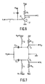
- FIG. 6 shows that this object is achieved by applying to the gate 20 of the transistor T1, the digital N and analog signals of frequency F0 by means of an element called "polarization T".
- FIG. 7 is based on the properties of the circuit of FIG. 5a explained in Example III, and proposes to apply these properties to the production of a 0-180 ° phase shifter.
- any transistor which is both of the field effect (unipolar) and insulated gate type can be used to make circuits according to examples I to IV.
- V GS when a high voltage V GS is applied to the gate of one of these transistors, a characteristic I DS is obtained as a function of V GS which shows a maximum (first derivative equal to zero) of on either side of which the slopes of the curve are substantially symmetrical so that two values of V GS symmetrical with respect to the maximum corresponds to a single value of the current I DS .
- V GS maximum (first derivative equal to zero) of on either side of which the slopes of the curve are substantially symmetrical so that two values of V GS symmetrical with respect to the maximum corresponds to a single value of the current I DS .
- V DD positive supply voltage
- the grid of field effect transistors can be produced in two different ways.
- the grid can be metallic for MISFETs (French: Metal-Insulator-Semiconductor-Field-Effect Transistor), or the grid may itself be a semiconductor material for SISFETs (Semiconductor-Insulator-Semiconductor-Field-Effect-transistor).
- MISFETs Metal-Insulator-Semiconductor-Field-Effect Transistor
- SISFETs semiconductor-Insulator-Semiconductor-Field-Effect-transistor
Landscapes
- Physics & Mathematics (AREA)
- Engineering & Computer Science (AREA)
- Computer Hardware Design (AREA)
- Computing Systems (AREA)
- General Engineering & Computer Science (AREA)
- Mathematical Physics (AREA)
- Junction Field-Effect Transistors (AREA)
- Metal-Oxide And Bipolar Metal-Oxide Semiconductor Integrated Circuits (AREA)
Applications Claiming Priority (4)
| Application Number | Priority Date | Filing Date | Title |
|---|---|---|---|
| FR8900809 | 1989-01-24 | ||
| FR8900810A FR2642226A1 (fr) | 1989-01-24 | 1989-01-24 | Dispositif semiconducteur integre incluant un etage ou-exclusif complementaire |
| FR8900809A FR2642225A1 (fr) | 1989-01-24 | 1989-01-24 | Dispositif semiconducteur integre incluant un circuit doubleur de frequences |
| FR8900810 | 1989-01-24 |
Publications (2)
| Publication Number | Publication Date |
|---|---|
| EP0380168A1 true EP0380168A1 (de) | 1990-08-01 |
| EP0380168B1 EP0380168B1 (de) | 1995-04-26 |
Family
ID=26227127
Family Applications (1)
| Application Number | Title | Priority Date | Filing Date |
|---|---|---|---|
| EP90200131A Expired - Lifetime EP0380168B1 (de) | 1989-01-24 | 1990-01-18 | Integrierte Halbleitervorrichtung, die einen Feldeffekt-Transistor mit isoliertem, auf einem erhöhtem Pegel vorgespanntem Gate enthält |
Country Status (5)
| Country | Link |
|---|---|
| US (1) | US5130763A (de) |
| EP (1) | EP0380168B1 (de) |
| JP (1) | JPH02237165A (de) |
| KR (1) | KR900012372A (de) |
| DE (1) | DE69018842T2 (de) |
Families Citing this family (30)
| Publication number | Priority date | Publication date | Assignee | Title |
|---|---|---|---|---|
| KR0137601B1 (ko) * | 1994-09-16 | 1998-04-28 | 양승택 | 전자의 간섭성을 이용한 양자간섭 트랜지스터 |
| US5767526A (en) * | 1997-01-07 | 1998-06-16 | Texas Instruments Incorporated | Bipolar resonant tunneling transistor frequency multiplier |
| JP2000049338A (ja) * | 1998-07-28 | 2000-02-18 | Mitsubishi Electric Corp | 絶縁ゲート型トランジスタの特性評価方法、絶縁ゲート型トランジスタの製造方法、絶縁ゲート型トランジスタの特性評価装置、および特性評価プログラムを記録してあるコンピュータ読み取り可能な記録媒体 |
| US6512274B1 (en) * | 2000-06-22 | 2003-01-28 | Progressant Technologies, Inc. | CMOS-process compatible, tunable NDR (negative differential resistance) device and method of operating same |
| US6596617B1 (en) | 2000-06-22 | 2003-07-22 | Progressant Technologies, Inc. | CMOS compatible process for making a tunable negative differential resistance (NDR) device |
| US6479862B1 (en) * | 2000-06-22 | 2002-11-12 | Progressant Technologies, Inc. | Charge trapping device and method for implementing a transistor having a negative differential resistance mode |
| US6754104B2 (en) * | 2000-06-22 | 2004-06-22 | Progressant Technologies, Inc. | Insulated-gate field-effect transistor integrated with negative differential resistance (NDR) FET |
| US6559470B2 (en) | 2000-06-22 | 2003-05-06 | Progressed Technologies, Inc. | Negative differential resistance field effect transistor (NDR-FET) and circuits using the same |
| US6518589B2 (en) | 2000-06-22 | 2003-02-11 | Progressant Technologies, Inc. | Dual mode FET & logic circuit having negative differential resistance mode |
| US6724655B2 (en) | 2000-06-22 | 2004-04-20 | Progressant Technologies, Inc. | Memory cell using negative differential resistance field effect transistors |
| US6594193B2 (en) | 2000-06-22 | 2003-07-15 | Progressent Technologies, Inc. | Charge pump for negative differential resistance transistor |
| US6956262B1 (en) | 2001-12-21 | 2005-10-18 | Synopsys Inc. | Charge trapping pull up element |
| US7453083B2 (en) * | 2001-12-21 | 2008-11-18 | Synopsys, Inc. | Negative differential resistance field effect transistor for implementing a pull up element in a memory cell |
| US7095659B2 (en) * | 2002-06-28 | 2006-08-22 | Progressant Technologies, Inc. | Variable voltage supply bias and methods for negative differential resistance (NDR) based memory device |
| US6853035B1 (en) * | 2002-06-28 | 2005-02-08 | Synopsys, Inc. | Negative differential resistance (NDR) memory device with reduced soft error rate |
| US6567292B1 (en) | 2002-06-28 | 2003-05-20 | Progressant Technologies, Inc. | Negative differential resistance (NDR) element and memory with reduced soft error rate |
| US6864104B2 (en) * | 2002-06-28 | 2005-03-08 | Progressant Technologies, Inc. | Silicon on insulator (SOI) negative differential resistance (NDR) based memory device with reduced body effects |
| US6912151B2 (en) * | 2002-06-28 | 2005-06-28 | Synopsys, Inc. | Negative differential resistance (NDR) based memory device with reduced body effects |
| US7098472B2 (en) * | 2002-06-28 | 2006-08-29 | Progressant Technologies, Inc. | Negative differential resistance (NDR) elements and memory device using the same |
| US6847562B2 (en) * | 2002-06-28 | 2005-01-25 | Progressant Technologies, Inc. | Enhanced read and write methods for negative differential resistance (NDR) based memory device |
| US6795337B2 (en) | 2002-06-28 | 2004-09-21 | Progressant Technologies, Inc. | Negative differential resistance (NDR) elements and memory device using the same |
| US6812084B2 (en) * | 2002-12-09 | 2004-11-02 | Progressant Technologies, Inc. | Adaptive negative differential resistance device |
| US7012833B2 (en) * | 2002-12-09 | 2006-03-14 | Progressant Technologies, Inc. | Integrated circuit having negative differential resistance (NDR) devices with varied peak-to-valley ratios (PVRs) |
| US6849483B2 (en) * | 2002-12-09 | 2005-02-01 | Progressant Technologies, Inc. | Charge trapping device and method of forming the same |
| US6980467B2 (en) * | 2002-12-09 | 2005-12-27 | Progressant Technologies, Inc. | Method of forming a negative differential resistance device |
| US6806117B2 (en) * | 2002-12-09 | 2004-10-19 | Progressant Technologies, Inc. | Methods of testing/stressing a charge trapping device |
| US6979580B2 (en) * | 2002-12-09 | 2005-12-27 | Progressant Technologies, Inc. | Process for controlling performance characteristics of a negative differential resistance (NDR) device |
| US7005711B2 (en) * | 2002-12-20 | 2006-02-28 | Progressant Technologies, Inc. | N-channel pull-up element and logic circuit |
| TW200826203A (en) * | 2006-12-14 | 2008-06-16 | Univ Nat Taiwan | Method for utilizing III-V semiconductors as gate electrode |
| US10958216B2 (en) * | 2019-08-22 | 2021-03-23 | Taiwan Semiconductor Manufacturing Co., Ltd. | Semiconductor device and operation method thereof |
Family Cites Families (11)
| Publication number | Priority date | Publication date | Assignee | Title |
|---|---|---|---|---|
| US4027179A (en) * | 1975-08-28 | 1977-05-31 | Rca Corporation | High repetition rate injection laser modulator |
| US4366493A (en) * | 1980-06-20 | 1982-12-28 | International Business Machines Corporation | Semiconductor ballistic transport device |
| US4605912A (en) * | 1981-12-03 | 1986-08-12 | General Electric Company | Continuously variable phase shifting element comprised of interdigitated electrode MESFET |
| US4636823A (en) * | 1984-06-05 | 1987-01-13 | California Institute Of Technology | Vertical Schottky barrier gate field-effect transistor in GaAs/GaAlAs |
| US4788579A (en) * | 1985-09-30 | 1988-11-29 | The General Electric Company | Semiconductor superlattice |
| JPH0611056B2 (ja) * | 1985-12-03 | 1994-02-09 | 富士通株式会社 | 高速半導体装置 |
| JPS62176162A (ja) * | 1986-01-30 | 1987-08-01 | Agency Of Ind Science & Technol | 負性抵抗素子 |
| US4724342A (en) * | 1986-02-12 | 1988-02-09 | Hughes Aircraft Company | Push-pull DCFL driver circuit |
| FR2600821B1 (fr) * | 1986-06-30 | 1988-12-30 | Thomson Csf | Dispositif semi-conducteur a heterojonction et double canal, son application a un transistor a effet de champ, et son application a un dispositif de transductance negative |
| US4885623A (en) * | 1987-10-30 | 1989-12-05 | Holm Kennedy James W | Distributed channel-bipolar device |
| US5021841A (en) * | 1988-10-14 | 1991-06-04 | University Of Illinois | Semiconductor device with controlled negative differential resistance characteristic |
-
1990
- 1990-01-18 DE DE69018842T patent/DE69018842T2/de not_active Expired - Fee Related
- 1990-01-18 EP EP90200131A patent/EP0380168B1/de not_active Expired - Lifetime
- 1990-01-19 US US07/467,625 patent/US5130763A/en not_active Expired - Fee Related
- 1990-01-24 KR KR1019900000805A patent/KR900012372A/ko not_active Withdrawn
- 1990-01-24 JP JP2012741A patent/JPH02237165A/ja active Pending
Non-Patent Citations (5)
| Title |
|---|
| ELECTRONICS LETTERS, vol. 23, no. 21, 8 octobre 1987, pages 1127,1128, Hitchin, GB; M. WOLNY et al.: "High-performance WN-gate MISFETs fabricated from MOVPE wafers" * |
| IBM TECHNICAL DISCLOSURE BULLETIN, vol. 7, no. 4, septembre 1964, page 337, New York, US; W.B. PENNEBAKER: "Frequency doubler" * |
| IEEE ELECTRON DEVICE LETTERS, vol. EDL-7, no. 2, fevrier 1986, pages 78-80, IEEE, New York, US; M.S. SHUR et al.: "New negative resistance regime of heterostructure insulated gate transistor (HIGFET) operation" * |
| INTERNATIONAL ELECTRON DEVICES MEETING, Washington, DC, 1-4 decembre 1985, Technical Digest, pages 317-320, IEEE, New York, US; N.C. CIRILLO et al.: "Complementary heterostructure insulated gate field effect transistors (HIGFETs)" * |
| JAPANESE JOURNAL OF APPLIED PHYSICS, vol. 24, no. 11, novembre 1985, pages L853 - L854, Japan Society of Physics, Tokyo, JP; N. YOKOYAMA et al.: "A new functional, resonant-tunneling hot electron transistor (RHET)" * |
Also Published As
| Publication number | Publication date |
|---|---|
| KR900012372A (ko) | 1990-08-04 |
| DE69018842T2 (de) | 1995-12-07 |
| EP0380168B1 (de) | 1995-04-26 |
| DE69018842D1 (de) | 1995-06-01 |
| JPH02237165A (ja) | 1990-09-19 |
| US5130763A (en) | 1992-07-14 |
Similar Documents
| Publication | Publication Date | Title |
|---|---|---|
| EP0380168B1 (de) | Integrierte Halbleitervorrichtung, die einen Feldeffekt-Transistor mit isoliertem, auf einem erhöhtem Pegel vorgespanntem Gate enthält | |
| JP3292894B2 (ja) | 集積化受光回路 | |
| EP0305253A1 (de) | Mikrowellentransistor mit Doppelheteroübergang | |
| EP0148706A2 (de) | Variables Impedanzglied und sein Regelkreis | |
| EP0149390B1 (de) | Feldeffekttransistor mit vertikaler Sub-Mikronstruktur und Verfahren zu dessen Herstellung | |
| FR2477338A1 (fr) | Circuit de sortie empeche de se bloquer du fait d'impulsions de tension produites par une charge inductive | |
| FR2489045A1 (fr) | Transistor a effet de champ gaas a memoire non volatile | |
| Razeghi et al. | Planar monolithic integrated photoreceiver for 1.3–1.55 μm wavelength applications using GaInAs‐GaAs heteroepitaxies | |
| EP0549043A1 (de) | Integrierte Schaltung mit einem Verstärker mit variabler Verstärkung | |
| EP0318379A1 (de) | Ultrahochfrequenzverstärker mit sehr breitem Durchlassbereich | |
| EP0120744B1 (de) | Analoger und aperiodischer Frequenzteiler für eine Teilung durch zwei | |
| EP0684653B1 (de) | Lichtgesteuerter Heterostruktur-Halbleiterbaustein zur Erzeugung von Mikrowellen | |
| EP0380166A1 (de) | Integrierte Halbleitervorrichtung die einen Feldeffekttransistor mit isoliertem, auf einem erhöhten Pegel vorgespannten Gate umfasst, um eine Zone mit negativer differentieller Leitfähigkeit der Drainelektrode zu erzeugen | |
| CA1296112C (fr) | Dispositif a semiconducteur organique a base de phtalocyanine | |
| FR2545989A1 (fr) | Transistor a effet de champ, fonctionnant en regime d'enrichissement | |
| US5670385A (en) | Method for fabricating an optical controlled resonant tunneling oscillator | |
| US4831428A (en) | Infrared ray detection device | |
| EP0204387B1 (de) | Halbleiteranordnung zur Herstellung der Entkupplungskapazitäten, die zwischen der Versorgung und der Erdung von integrierten Schaltungen liegen | |
| EP0259207B1 (de) | Stromquelle mit aktiver Ladung und Verfahren zu ihrer Ausführung | |
| EP0305228B1 (de) | Feldeffekt-Halbleiteranordnung mit einer Nebenelektrode | |
| FR2642225A1 (fr) | Dispositif semiconducteur integre incluant un circuit doubleur de frequences | |
| EP0128061B1 (de) | Feldeffekttransistor des Verarmungstyps | |
| EP0093086A2 (de) | Bipolare Halbleiteranordnung und MOS-Schaltung mit solch einer Anordnung | |
| JPS60219766A (ja) | 半導体装置 | |
| FR2642226A1 (fr) | Dispositif semiconducteur integre incluant un etage ou-exclusif complementaire |
Legal Events
| Date | Code | Title | Description |
|---|---|---|---|
| PUAI | Public reference made under article 153(3) epc to a published international application that has entered the european phase |
Free format text: ORIGINAL CODE: 0009012 |
|
| AK | Designated contracting states |
Kind code of ref document: A1 Designated state(s): DE FR GB IT |
|
| 17P | Request for examination filed |
Effective date: 19910130 |
|
| 17Q | First examination report despatched |
Effective date: 19930706 |
|
| GRAA | (expected) grant |
Free format text: ORIGINAL CODE: 0009210 |
|
| AK | Designated contracting states |
Kind code of ref document: B1 Designated state(s): DE FR GB IT |
|
| REF | Corresponds to: |
Ref document number: 69018842 Country of ref document: DE Date of ref document: 19950601 |
|
| ITF | It: translation for a ep patent filed | ||
| GBT | Gb: translation of ep patent filed (gb section 77(6)(a)/1977) |
Effective date: 19950703 |
|
| REG | Reference to a national code |
Ref country code: FR Ref legal event code: CJ Ref country code: FR Ref legal event code: CD |
|
| PLBE | No opposition filed within time limit |
Free format text: ORIGINAL CODE: 0009261 |
|
| STAA | Information on the status of an ep patent application or granted ep patent |
Free format text: STATUS: NO OPPOSITION FILED WITHIN TIME LIMIT |
|
| 26N | No opposition filed | ||
| PGFP | Annual fee paid to national office [announced via postgrant information from national office to epo] |
Ref country code: GB Payment date: 19990122 Year of fee payment: 10 |
|
| PGFP | Annual fee paid to national office [announced via postgrant information from national office to epo] |
Ref country code: FR Payment date: 19990126 Year of fee payment: 10 |
|
| PGFP | Annual fee paid to national office [announced via postgrant information from national office to epo] |
Ref country code: DE Payment date: 19990325 Year of fee payment: 10 |
|
| PG25 | Lapsed in a contracting state [announced via postgrant information from national office to epo] |
Ref country code: GB Free format text: LAPSE BECAUSE OF NON-PAYMENT OF DUE FEES Effective date: 20000118 |
|
| GBPC | Gb: european patent ceased through non-payment of renewal fee |
Effective date: 20000118 |
|
| PG25 | Lapsed in a contracting state [announced via postgrant information from national office to epo] |
Ref country code: FR Free format text: LAPSE BECAUSE OF NON-PAYMENT OF DUE FEES Effective date: 20000929 |
|
| PG25 | Lapsed in a contracting state [announced via postgrant information from national office to epo] |
Ref country code: DE Free format text: LAPSE BECAUSE OF NON-PAYMENT OF DUE FEES Effective date: 20001101 |
|
| REG | Reference to a national code |
Ref country code: FR Ref legal event code: ST |
|
| PG25 | Lapsed in a contracting state [announced via postgrant information from national office to epo] |
Ref country code: IT Free format text: LAPSE BECAUSE OF NON-PAYMENT OF DUE FEES;WARNING: LAPSES OF ITALIAN PATENTS WITH EFFECTIVE DATE BEFORE 2007 MAY HAVE OCCURRED AT ANY TIME BEFORE 2007. THE CORRECT EFFECTIVE DATE MAY BE DIFFERENT FROM THE ONE RECORDED. Effective date: 20050118 |