EP0380322B1 - Lasers à semi-conducteurs - Google Patents
Lasers à semi-conducteurs Download PDFInfo
- Publication number
- EP0380322B1 EP0380322B1 EP90300747A EP90300747A EP0380322B1 EP 0380322 B1 EP0380322 B1 EP 0380322B1 EP 90300747 A EP90300747 A EP 90300747A EP 90300747 A EP90300747 A EP 90300747A EP 0380322 B1 EP0380322 B1 EP 0380322B1
- Authority
- EP
- European Patent Office
- Prior art keywords
- layer
- upper portion
- cladding layer
- portion cladding
- semiconductor substrate
- Prior art date
- Legal status (The legal status is an assumption and is not a legal conclusion. Google has not performed a legal analysis and makes no representation as to the accuracy of the status listed.)
- Expired - Lifetime
Links
- 239000004065 semiconductor Substances 0.000 title claims description 54
- 238000005253 cladding Methods 0.000 claims description 99
- 239000000758 substrate Substances 0.000 claims description 49
- 238000000034 method Methods 0.000 claims description 37
- 238000001704 evaporation Methods 0.000 claims description 34
- 230000031700 light absorption Effects 0.000 claims description 30
- 230000008020 evaporation Effects 0.000 claims description 27
- 238000004519 manufacturing process Methods 0.000 claims description 11
- 238000010276 construction Methods 0.000 claims description 10
- 239000012535 impurity Substances 0.000 claims description 8
- 238000001259 photo etching Methods 0.000 claims description 7
- 229910001218 Gallium arsenide Inorganic materials 0.000 description 17
- 239000002019 doping agent Substances 0.000 description 5
- 229920002120 photoresistant polymer Polymers 0.000 description 5
- 238000001451 molecular beam epitaxy Methods 0.000 description 4
- ZOKXTWBITQBERF-UHFFFAOYSA-N Molybdenum Chemical compound [Mo] ZOKXTWBITQBERF-UHFFFAOYSA-N 0.000 description 2
- 238000000137 annealing Methods 0.000 description 2
- 238000004871 chemical beam epitaxy Methods 0.000 description 2
- 238000001741 metal-organic molecular beam epitaxy Methods 0.000 description 2
- 229910052750 molybdenum Inorganic materials 0.000 description 2
- 239000011733 molybdenum Substances 0.000 description 2
- 239000002994 raw material Substances 0.000 description 2
- 239000001852 Succistearin Substances 0.000 description 1
- 238000005229 chemical vapour deposition Methods 0.000 description 1
- 230000008602 contraction Effects 0.000 description 1
- 238000007796 conventional method Methods 0.000 description 1
- 238000009792 diffusion process Methods 0.000 description 1
- 238000010438 heat treatment Methods 0.000 description 1
- 230000000717 retained effect Effects 0.000 description 1
Images


Classifications
-
- H—ELECTRICITY
- H10—SEMICONDUCTOR DEVICES; ELECTRIC SOLID-STATE DEVICES NOT OTHERWISE PROVIDED FOR
- H10H—INORGANIC LIGHT-EMITTING SEMICONDUCTOR DEVICES HAVING POTENTIAL BARRIERS
- H10H20/00—Individual inorganic light-emitting semiconductor devices having potential barriers, e.g. light-emitting diodes [LED]
- H10H20/01—Manufacture or treatment
- H10H20/011—Manufacture or treatment of bodies, e.g. forming semiconductor layers
- H10H20/013—Manufacture or treatment of bodies, e.g. forming semiconductor layers having light-emitting regions comprising only Group III-V materials
-
- H—ELECTRICITY
- H01—ELECTRIC ELEMENTS
- H01S—DEVICES USING THE PROCESS OF LIGHT AMPLIFICATION BY STIMULATED EMISSION OF RADIATION [LASER] TO AMPLIFY OR GENERATE LIGHT; DEVICES USING STIMULATED EMISSION OF ELECTROMAGNETIC RADIATION IN WAVE RANGES OTHER THAN OPTICAL
- H01S5/00—Semiconductor lasers
- H01S5/20—Structure or shape of the semiconductor body to guide the optical wave ; Confining structures perpendicular to the optical axis, e.g. index or gain guiding, stripe geometry, broad area lasers, gain tailoring, transverse or lateral reflectors, special cladding structures, MQW barrier reflection layers
- H01S5/22—Structure or shape of the semiconductor body to guide the optical wave ; Confining structures perpendicular to the optical axis, e.g. index or gain guiding, stripe geometry, broad area lasers, gain tailoring, transverse or lateral reflectors, special cladding structures, MQW barrier reflection layers having a ridge or stripe structure
- H01S5/223—Buried stripe structure
- H01S5/2231—Buried stripe structure with inner confining structure only between the active layer and the upper electrode
-
- H—ELECTRICITY
- H01—ELECTRIC ELEMENTS
- H01S—DEVICES USING THE PROCESS OF LIGHT AMPLIFICATION BY STIMULATED EMISSION OF RADIATION [LASER] TO AMPLIFY OR GENERATE LIGHT; DEVICES USING STIMULATED EMISSION OF ELECTROMAGNETIC RADIATION IN WAVE RANGES OTHER THAN OPTICAL
- H01S5/00—Semiconductor lasers
- H01S5/30—Structure or shape of the active region; Materials used for the active region
- H01S5/32—Structure or shape of the active region; Materials used for the active region comprising PN junctions, e.g. hetero- or double- heterostructures
-
- H—ELECTRICITY
- H01—ELECTRIC ELEMENTS
- H01S—DEVICES USING THE PROCESS OF LIGHT AMPLIFICATION BY STIMULATED EMISSION OF RADIATION [LASER] TO AMPLIFY OR GENERATE LIGHT; DEVICES USING STIMULATED EMISSION OF ELECTROMAGNETIC RADIATION IN WAVE RANGES OTHER THAN OPTICAL
- H01S5/00—Semiconductor lasers
- H01S5/30—Structure or shape of the active region; Materials used for the active region
- H01S5/32—Structure or shape of the active region; Materials used for the active region comprising PN junctions, e.g. hetero- or double- heterostructures
- H01S5/3211—Structure or shape of the active region; Materials used for the active region comprising PN junctions, e.g. hetero- or double- heterostructures characterised by special cladding layers, e.g. details on band-discontinuities
-
- H—ELECTRICITY
- H01—ELECTRIC ELEMENTS
- H01S—DEVICES USING THE PROCESS OF LIGHT AMPLIFICATION BY STIMULATED EMISSION OF RADIATION [LASER] TO AMPLIFY OR GENERATE LIGHT; DEVICES USING STIMULATED EMISSION OF ELECTROMAGNETIC RADIATION IN WAVE RANGES OTHER THAN OPTICAL
- H01S5/00—Semiconductor lasers
- H01S5/30—Structure or shape of the active region; Materials used for the active region
- H01S5/32—Structure or shape of the active region; Materials used for the active region comprising PN junctions, e.g. hetero- or double- heterostructures
- H01S5/323—Structure or shape of the active region; Materials used for the active region comprising PN junctions, e.g. hetero- or double- heterostructures in AIIIBV compounds, e.g. AlGaAs-laser, InP-based laser
- H01S5/32308—Structure or shape of the active region; Materials used for the active region comprising PN junctions, e.g. hetero- or double- heterostructures in AIIIBV compounds, e.g. AlGaAs-laser, InP-based laser emitting light at a wavelength less than 900 nm
-
- Y—GENERAL TAGGING OF NEW TECHNOLOGICAL DEVELOPMENTS; GENERAL TAGGING OF CROSS-SECTIONAL TECHNOLOGIES SPANNING OVER SEVERAL SECTIONS OF THE IPC; TECHNICAL SUBJECTS COVERED BY FORMER USPC CROSS-REFERENCE ART COLLECTIONS [XRACs] AND DIGESTS
- Y10—TECHNICAL SUBJECTS COVERED BY FORMER USPC
- Y10S—TECHNICAL SUBJECTS COVERED BY FORMER USPC CROSS-REFERENCE ART COLLECTIONS [XRACs] AND DIGESTS
- Y10S148/00—Metal treatment
- Y10S148/071—Heating, selective
-
- Y—GENERAL TAGGING OF NEW TECHNOLOGICAL DEVELOPMENTS; GENERAL TAGGING OF CROSS-SECTIONAL TECHNOLOGIES SPANNING OVER SEVERAL SECTIONS OF THE IPC; TECHNICAL SUBJECTS COVERED BY FORMER USPC CROSS-REFERENCE ART COLLECTIONS [XRACs] AND DIGESTS
- Y10—TECHNICAL SUBJECTS COVERED BY FORMER USPC
- Y10S—TECHNICAL SUBJECTS COVERED BY FORMER USPC CROSS-REFERENCE ART COLLECTIONS [XRACs] AND DIGESTS
- Y10S148/00—Metal treatment
- Y10S148/094—Laser beam treatment of compound devices
-
- Y—GENERAL TAGGING OF NEW TECHNOLOGICAL DEVELOPMENTS; GENERAL TAGGING OF CROSS-SECTIONAL TECHNOLOGIES SPANNING OVER SEVERAL SECTIONS OF THE IPC; TECHNICAL SUBJECTS COVERED BY FORMER USPC CROSS-REFERENCE ART COLLECTIONS [XRACs] AND DIGESTS
- Y10—TECHNICAL SUBJECTS COVERED BY FORMER USPC
- Y10S—TECHNICAL SUBJECTS COVERED BY FORMER USPC CROSS-REFERENCE ART COLLECTIONS [XRACs] AND DIGESTS
- Y10S148/00—Metal treatment
- Y10S148/095—Laser devices
Definitions
- the present invention relates to a semiconductor laser having a multi-layer construction for lowering the forward voltage.
- FIG 8 of the accompanying drawings a semiconductor laser 21, produced by such a technique, is shown and which has a lower portion cladding layer 23 composed of N type Al x Ga 1-x As, an active layer 24 composed of Al x' Ga 1-x As, a first upper portion cladding layer 25 composed of P type Al x Ga 1-x As, a light absorption layer 26 composed of N type GaAs, and an evaporation preventing layer 27 composed of N type Al x Ga 1-x As which are laminated on, for example, an N type GaAs type substrate 22.
- These respective layers 23 through 27 are formed by the use of conventional apparatus in a known manner.
- a strip groove 29 is formed by means of photo etching from the evaporation preventing layer 27 to the light absorption layer 26. Furthermore, a second upper portion cladding layer 30 composed of P type Al y Ga 1-y As and a cap layer 31 composed of P+ type Ga As are laminated as a regrowth by means of a conventional method. The first upper portion cladding layer 25 and the second upper portion cladding layer 30 come into contact with each other in the strip groove 29. Electrodes 32a and 32b are formed respectively on the substrate 22 and the cap layer 31.
- a known method of manufacturing such a GaAs semiconductor laser comprises:
- This problem can be overcome by an increase in the carrier concentration of the first upper portion cladding layer.
- the carrier concentration of the first upper portion cladding layer is increased, there is a problem that the other characteristics such as threshold current I th and so on are reduced.
- the present invention has been developed to substantially eliminate the above discussed drawbacks inherent in the prior art semiconductor laser and method of manufacture.
- the present invention provides a semiconductor laser having a multi-layer construction, which comprises a lower portion cladding layer, an active layer, a first upper portion cladding layer, a light absorption layer and an evaporation preventing layer which are laminated on a semiconductor substrate, a strip groove which reaches to the first upper portion cladding layer through the evaporation preventing layer, a second upper portion cladding layer and a cap layer which cover the strip groove, and electrodes which are provided on the semiconductor substrate and the cap layer, characterised in that the first upper portion cladding layer is of a double construction of which the upper layer portion is higher in carrier concentration than the lower layer portion.
- the series resistance portion may be reduced, the forward voltage V F may be lowered. Also, since the carrier concentration is higher in the first upper portion cladding layer in the upper layer portion only, the danger of damaging the other characteristics such as the threshold current I th, and so on is restricted.
- the invention provides a semiconductor laser having a multi-layer construction, which comprises a lower portion cladding layer, an active layer, a first upper portion cladding layer, a light absorption layer and an evaporation preventing layer which are laminated on a semiconductor substrate, a strip groove which reaches to the first upper portion cladding layer through the evaporation preventing layer, a second upper portion cladding layer and a cap layer which cover the strip groove, and electrodes which are provided on the semiconductor substrate and the cap layer, characterised in that the carrier concentration of the second upper portion cladding layer is higher than the carrier concentration of the first upper portion cladding layer, and the first upper portion cladding layer has an upper boundary portion with a higher carrier concentration than the rest of the first upper portion cladding layer.
- the invention provides a method of manufacturing semiconductor lasers comprising: a first growth process, wherein a lower portion cladding layer, an active layer, a first upper portion cladding layer, a light absorption layer and an evaporation preventing layer are laminated on a semiconductor substrate introduced into the growth chamber of an apparatus; a photo-etching process, wherein the laminated semiconductor substrate is taken out of the growth chamber, and a strip groove deep enough to reach down to the light absorption layer is formed; a re-evaporation process, wherein the semiconductor substrate with the strip groove is introduced into the growth chamber of the apparatus to heat the semiconductor substrate so as to selectively evaporate the light absorption layer; and a second growth process, wherein a second upper portion cladding layer and a cap layer are laminated on the semiconductor substrate with the impurities being evaporated; characterised in that, in the first growth process, the first upper portion cladding layer is formed as a two-layer construction of which the upper layer portion is higher in carrier concentration than the lower layer portion.
- the present invention provides a method of manufacturing semiconductor laser comprising: a first growth process, wherein a lower portion cladding layer, an active layer, a first upper portion cladding layer, a light absorption layer, and an evaporation preventing layer are laminated on a semiconductor substrate introduced into the growth chamber of an apparatus; a photo-etching process, wherein the laminated semiconductor substrate is taken out of growth chamber, and a strip groove deep enough to reach down to the light absorption layer is formed; a re-evaporation process, wherein the semiconductor substrate with the strip groove is introduced into the growth chamber of the apparatus to heat the semiconductor substrate so as to selectively evaporate the light absorption layer; and a second growth process, wherein a second upper portion cladding layer and a cap layer are laminated on the semiconductor substrate with the impurities being evaporated; characterised in that in the second growth process, the carrier concentration of the second upper portion cladding layer is made higher than the carrier concentration of the first upper portion cladding layer in which, after the growth of the
- the carrier concentration of the second upper portion cladding layer is made higher, dopant diffuses from the second upper portion cladding layer to the first upper portion cladding layer when heating is effected for the given time. Therefore, the carrier concentration is increased only in the boundary portion of the first upper portion cladding layer and the series resistance component is reduced to lower the forward voltage V F . Since the carrier concentration is increased in the first upper portion cladding layer on the boundary portion only, the danger of damaging the other characteristics such as the threshold current I th and so on is reduced.
- MOCVD Chemical Vapor Deposition
- CBE Chemical Beam Epitaxy
- MOMBE Metal-organic Molecular Beam Epitaxy
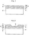
- Figure 3 illustrates a multi-layer semiconductor laser 1 which comprises a substrate 2, a lower portion cladding layer 3, an active layer 4, a first upper portion cladding layer 5 with a lower layer portion 5a and an upper layer portion 5b, a light absorption layer 6, an evaporation preventing layer 7, a strip groove 9, a second upper portion cladding layer 10, a cap layer 11, and electrodes 12a and 12b.
- Figures 1 and 2 illustrate views during the manufacturing process of the semiconductor laser 1.
- the N type GaAs substrate 2 is prepared, is engaged with a molybdenum stand of an apparatus for use in a molecular beam epitaxy process (not shown), and is heated.
- a molybdenum stand of an apparatus for use in a molecular beam epitaxy process (not shown), and is heated.
- raw materials and impurities, that is dopant put into the evaporation source are evaporated in the shape of molecular beams.
- the shutter of the evaporation source is controlled, and the respective layers 3 to 7 are formed.
- the first upper portion cladding layer 5 is of a double layer construction comprising the upper layer 5b and the lower layer 5a.
- the upper layer 5b is assumed to be higher in the carrier concentration than the lower layer 5a.
- the value of X for Al is not restricted to the above-described numerical value, but is variable.
- the substrate 2 is taken out of the apparatus and the evaporation preventing layer 7, except for the portion where the strip groove is to be formed, is covered with a photo resist 8, as shown in Figure 2.
- the photoresist 8 as a mask, the evaporation preventing layer 7 and the light absorption layer 6 are respectively etched selectively to form the strip groove 9. At this time, a thin strip of the light absorption layer 6 remains at the base of the groove 9.
- the photoresist 8 is removed from the substrate 2 and the substrate 2 is placed within the apparatus again and is heated to a temperature of between 650° to 800°C, preferably approximately 760°C, with the As molecular beams being directed upon it.
- the thin strip of the light absorption layer 6 left is evaporated, and the upper layer portion 5b of the first upper portion cladding layer 5 is exposed within the strip groove 9.
- the second upper portion cladding layer 10 composed of P type Al y Ga 1-y As is formed so as to cover the evaporation preventing layer 7 and the strip groove 9.
- the value of the Y is assumed to be, for example, 0.6.
- the cap layer 11 composed of P+ type GaAs is formed on the second upper portion cladding layer 10.
- the electrodes 12a and 12b are respectively provided on the under face of the substrate 2 and the cap layer 11 surface to complete the semiconductor laser 1 (see Figure 3).
- the sequential direction voltage V F may be restrained lower, for instance, less than 2V. Also, since the carrier concentration of the first upper portion cladding layer 5 as a whole is not high, the other characteristics such as the threshold current I th and so on are not damaged, either.
- Figures 4 to 7 illustrate another process of manufacturing a semiconductor laser which comprises the following four processes a to d.
- an N type GaAs substrate 2 engaged with a molybdenum block is introduced into a growth chamber of an apparatus for use in a molecular beam epitaxy process.
- raw materials and impurities, that is dopant put into the evaporation source are evaporated in the shape of molecular beams.
- the shutter of the evaporation source is restrained, and the respective layers 3 to 7 given hereinafter are sequentially grown, as shown in Figure 4.
- the value of X in Al shown hereinbefore is only an example and is variable.
- the laminated GaAs substrate 2 is taken out from within the apparatus growth chamber, thereafter the evaporation preventing layer 7, except for the portion to be formed with a groove in it, is covered with a photoresist 8, as shown in Figure 5.
- the evaporation preventing layer 7 and the light absorption layer 6 are respectively etched to form a strip groove 9 so that a thin layer of the light absorption layer 6 may be left, at the base of the groove for example, approximately 1000 ⁇ (1 x 10 ⁇ 7m, 10 ⁇ m).
- the GaAs substrate 2 is introduced again into the apparatus growth chamber to heat the GaAs substrate 2 to a temperature of between approximately 650°C to 850°C with the As molecular beams being directed upon it.
- the impurities attached onto the GaAs substrate are evaporated during this period, also the remainder of the light absorption layer 6 is also evaporated to expose the first upper portion cladding layer 5 at the base of the strip groove 9.
- the second upper cladding layer 10 is grown on the GaAs substrate 2, as shown in Figure 6.
- the carrier concentration of the first upper portion cladding layer 5 is 3 X 1017 cm ⁇ 3
- the carrier concentration of the second upper portion cladding layer is assumed to be approximately 3 x 1018 cm ⁇ 3.
- the temperature of the GaAs substrate 2 is raised again to between 650°C to 850°C, preferably approximately 760°C, and is retained at that temperature for between several minutes to several tens of minutes, for instance, about 20 minutes.
- the dopant diffuses from the second upper portion cladding layer 10 to the first upper portion cladding layer 5 to increase the carrier concentration of the upper portion cladding layer boundary portion 5c to, for example, a value of about 8 x 10¹⁷ to 1 x 1018 cm ⁇ 3.
- a cap layer 11 composed of the P+ type GaAs is grown on the second upper portion cladding layer 10 and electrodes 12a and 12b are provided, as shown in Figure 7.
- the semiconductor laser 1 provided has a higher carrier concentration in the first upper portion cladding layer boundary portion 5c, the series resistance component may be restrained, and the forward voltage V F is lowered.
- the carrier concentration of a portion except for the boundary portion 5c of the first upper portion cladding layer 5 remains as it was conventionally, the other characteristics such as threshold current I th, and so on are not damaged.
- the diffusion of the dopant from the second upper portion cladding layer 10 to the first upper portion cladding layer 5 may be effected within the apparatus growth chamber.
Landscapes
- Physics & Mathematics (AREA)
- Condensed Matter Physics & Semiconductors (AREA)
- General Physics & Mathematics (AREA)
- Electromagnetism (AREA)
- Optics & Photonics (AREA)
- Geometry (AREA)
- Semiconductor Lasers (AREA)
- Physical Deposition Of Substances That Are Components Of Semiconductor Devices (AREA)
Claims (4)
- Laser à semiconducteur possédant une structure multicouche, qui comprend une couche de revêtement de partie inférieure (3), une couche active (4), une première couche de revêtement de partie supérieure (5), une couche d'absorption de lumière (6) et une couche (7) destinée à empêcher l'évaporation, ou couche anti-évaporation, lesquelles couches sont placées de manière stratifiée sur un substrat semiconducteur (2), une rainure de mise à nu (9) qui atteint la première couche de revêtement de partie supérieure (5) au travers de la couche anti-évaporation (7), une deuxième couche de revêtement de partie supérieure (10) et une couche de couverture (11) qui couvrent la rainure de mise à nu (9), et des électrodes (12a, 12b) qui sont placées sur le substrat semiconducteur (2) et sur la couche de couverture (11), caractérisé en ce que la première couche de revêtement de partie supérieure (5) présente une double structure (5a, 5b) dans laquelle la partie de couche supérieure (5b) a une plus forte concentration en porteurs que la partie de couche inférieure (5a).
- Laser à semiconducteur possédant une structure multicouche, qui comprend une couche de revêtement de partie inférieure (3), une couche active (4), une première couche de revêtement de partie supérieure (5), une couche d'absorption de lumière (6) et une couche (7) destinée à empêcher l'évaporation, ou couche anti-évaporation, lesquelles couches sont placées de manière stratifiée sur un substrat semiconducteur (2), une rainure de mise à nu (9) qui atteint la première couche de revêtement de partie supérieure (5) au travers de la couche anti-évaporation (7), une deuxième couche de revêtement de partie supérieure (10) et une couche de couverture (11) qui couvrent la rainure de mise à nu (9), et des électrodes (12a, 12b) qui sont placées sur le substrat semiconducteur (2) et sur la couche de couverture (11), caractérisé en ce que la concentration en porteurs de la deuxième couche de revêtement de partie supérieure (10) est plus élevée que celle de la première couche de revêtement de partie supérieure (5), et la première couche de revêtement de partie supérieure (5) possède une partie frontière supérieure (5c) ayant une concentration en porteurs plus élevée que le reste de la première couche de revêtement de partie supérieure (5).
- Procédé de fabrication de lasers à semiconducteur, comprenant: un premier processus de croissance, où on forme de manière stratifiée, sur un substrat semiconducteur (2) qui a été introduit dans la chambre de croissance d'un appareil, une couche de revêtement de partie inférieure (3), une couche active (4), une première couche de revêtement de partie supérieure (5), une couche d'absorption de lumière (6) et une couche (7) destinée à empêcher l'évaporation, ou couche anti-évaporation ;
un processus de photogravure, où on sort le substrat semiconducteur (2) ainsi stratifié hors de la chambre de croissance et on forme une rainure de mise à nu (9) suffisamment profonde pour atteindre la couche d'absorption de lumière (6);
un processus de ré-évaporation, où on introduit le substrat semiconducteur (2) doté de la rainure de mise à nu (9) dans la chambre de croissance de l'appareil pour chauffer le substrat semiconducteur (2) de façon à faire sélectivement évaporer la couche d'absorption de lumière (6); et
un deuxième processus de croissance, où on fait déposer de manière stratifiée une deuxième couche de revêtement de partie supérieure (10) et une couche de couverture (11) sur le substrat semiconducteur (2) dans lequel les impuretés se sont évaporées;
caractérisé en ce que, dans le premier processus de croissance, on forme la première couche de revêtement de partie supérieure (5) suivant une structure à deux couches (5a, 5b) dans laquelle la partie de couche supérieure (5b) a une concentration en porteurs plus élevée que la partie de couche inférieure (5a). - Procédé de fabrication de lasers à semiconducteur, comprenant: un premier processus de croissance, où on forme de manière stratifiée, sur un substrat semiconducteur (2) qui a été introduit dans la chambre de croissance d'un appareil, une couche de revêtement de partie inférieure (3), une couche active (4), une première couche de revêtement de partie supérieure (5), une couche d'absorption de lumière (6) et une couche (7) destinée à empêcher l'évaporation, ou couche anti-évaporation ;
un processus de photogravure, où on sort le substrat semiconducteur (2) ainsi stratifié hors de la chambre de croissance et on forme une rainure de mise à nu (9) suffisamment profonde pour atteindre la couche d'absorption de lumière (6);
un processus de ré-évaporation, où on introduit le substrat semiconducteur (2) doté de la rainure de mise à nu (9) dans la chambre de croissance de l'appareil pour chauffer le substrat semiconducteur (2) de façon à faire sélectivement évaporer la couche d'absorption de lumière (6); et
un deuxième processus de croissance, où on fait déposer de manière stratifiée une deuxième couche de revêtement de partie supérieure (10) et une couche de couverture (11) sur le substrat semiconducteur (2) dans lequel les impuretés se sont évaporées;
caractérisé en ce que, dans le deuxième processus de croissance, la concentration en porteurs de la deuxième couche de revêtement de partie supérieure (10) est établie à une valeur plus élevée que la concentration en porteurs de la première couche de revêtement de partie supérieure (5), où, après la croissance de la deuxième couche de revêtement de partie supérieure, on chauffe le substrat semiconducteur pendant une durée donnée dans la chambre de croissance à l'intérieur de l'appareil avant qu'on ait fait croître la couche de couverture, si bien que la première couche de revêtement de partie supérieure (5) possède une partie frontière supérieure (5c) ayant une concentration en porteurs supérieure au reste de la première couche de revêtement de partie supérieure (5).
Applications Claiming Priority (4)
| Application Number | Priority Date | Filing Date | Title |
|---|---|---|---|
| JP14345/89 | 1989-01-24 | ||
| JP14348/89 | 1989-01-24 | ||
| JP1014348A JPH0656911B2 (ja) | 1989-01-24 | 1989-01-24 | 半導体レーザの製造方法 |
| JP1014345A JPH02194681A (ja) | 1989-01-24 | 1989-01-24 | 半導体レーザ |
Publications (3)
| Publication Number | Publication Date |
|---|---|
| EP0380322A2 EP0380322A2 (fr) | 1990-08-01 |
| EP0380322A3 EP0380322A3 (fr) | 1991-04-17 |
| EP0380322B1 true EP0380322B1 (fr) | 1993-12-15 |
Family
ID=26350268
Family Applications (1)
| Application Number | Title | Priority Date | Filing Date |
|---|---|---|---|
| EP90300747A Expired - Lifetime EP0380322B1 (fr) | 1989-01-24 | 1990-01-24 | Lasers à semi-conducteurs |
Country Status (6)
| Country | Link |
|---|---|
| US (2) | US4999841A (fr) |
| EP (1) | EP0380322B1 (fr) |
| KR (1) | KR930004128B1 (fr) |
| CA (1) | CA2008379C (fr) |
| DE (1) | DE69005132T2 (fr) |
| MY (1) | MY104857A (fr) |
Families Citing this family (14)
| Publication number | Priority date | Publication date | Assignee | Title |
|---|---|---|---|---|
| MY104857A (en) * | 1989-01-24 | 1994-06-30 | Rohm Co Ltd | Semiconductor lasers |
| JP2706369B2 (ja) * | 1990-11-26 | 1998-01-28 | シャープ株式会社 | 化合物半導体の成長方法及び半導体レーザの製造方法 |
| US5274656A (en) * | 1991-06-12 | 1993-12-28 | Sumitomo Electric Industries, Ltd. | Semiconductor laser |
| FR2684805B1 (fr) * | 1991-12-04 | 1998-08-14 | France Telecom | Dispositif optoelectronique a tres faible resistance serie. |
| GB2265755B (en) * | 1992-03-31 | 1995-11-08 | Matsushita Electronics Corp | Semiconductor laser device and its fabrication method |
| JPH0750445A (ja) * | 1993-06-02 | 1995-02-21 | Rohm Co Ltd | 半導体レーザの製法 |
| US6996150B1 (en) | 1994-09-14 | 2006-02-07 | Rohm Co., Ltd. | Semiconductor light emitting device and manufacturing method therefor |
| US6400743B1 (en) * | 1999-08-05 | 2002-06-04 | Fuji Photo Film Co., Ltd. | High-power semiconductor laser device having current confinement structure and index-guided structure |
| US20040010446A1 (en) * | 2002-07-08 | 2004-01-15 | Marko Vanska | Mobile customer relationship management |
| US7274909B2 (en) * | 2002-10-31 | 2007-09-25 | Nokia Corporation | Method and system for selecting data items for service requests |
| US7072672B1 (en) * | 2002-11-01 | 2006-07-04 | Nokia Corporation | Disposable mini-applications |
| US7407107B2 (en) | 2003-12-08 | 2008-08-05 | Nokia Corporation | Apparatus, system, method and computer program product for creating shortcuts to functions in a personal communication device |
| US7304585B2 (en) | 2004-07-02 | 2007-12-04 | Nokia Corporation | Initiation of actions with compressed action language representations |
| HK1204142A1 (en) * | 2012-03-30 | 2015-11-06 | 帝人株式会社 | Semiconductor laminate and method for manufacturing same, method for manufacturing semiconductor device, semiconductor device, dopant composition, dopant injection layer, and method for forming doped layer |
Family Cites Families (15)
| Publication number | Priority date | Publication date | Assignee | Title |
|---|---|---|---|---|
| JPS609356B2 (ja) * | 1975-08-28 | 1985-03-09 | 富士通株式会社 | 半導体発光装置の製法 |
| JPS59227179A (ja) * | 1983-06-08 | 1984-12-20 | Hitachi Ltd | 半導体レ−ザ装置及びその製造方法 |
| JPS6014482A (ja) * | 1983-07-04 | 1985-01-25 | Toshiba Corp | 半導体レ−ザ装置 |
| JPS6042885A (ja) * | 1983-08-19 | 1985-03-07 | Hitachi Ltd | 半導体レ−ザ装置 |
| JPS60110188A (ja) * | 1983-11-18 | 1985-06-15 | Sharp Corp | 半導体レ−ザ素子 |
| JPS61166090A (ja) * | 1985-01-17 | 1986-07-26 | Rohm Co Ltd | 半導体レ−ザの製造方法 |
| US4728707A (en) * | 1985-03-18 | 1988-03-01 | Daikin Industries Ltd. | Water- and oil-repellent |
| JPH06101433B2 (ja) * | 1985-04-22 | 1994-12-12 | 日本電気株式会社 | 半導体素子の製造方法 |
| DE68909632T2 (de) * | 1988-02-09 | 1994-03-10 | Toshiba Kawasaki Kk | Halbleiterlaser-Vorrichtung und deren Herstellungsverfahren. |
| JPH01220492A (ja) * | 1988-02-26 | 1989-09-04 | Mitsubishi Electric Corp | 半導体レーザ装置及びその製造方法 |
| JPH0221683A (ja) * | 1988-07-08 | 1990-01-24 | Mitsubishi Electric Corp | 半導体レーザ装置 |
| GB2222307B (en) * | 1988-07-22 | 1992-04-01 | Mitsubishi Electric Corp | Semiconductor laser |
| US4962057A (en) * | 1988-10-13 | 1990-10-09 | Xerox Corporation | Method of in situ photo induced evaporation enhancement of compound thin films during or after epitaxial growth |
| MY104857A (en) * | 1989-01-24 | 1994-06-30 | Rohm Co Ltd | Semiconductor lasers |
| US4980314A (en) * | 1989-06-06 | 1990-12-25 | At&T Bell Laboratories | Vapor processing of a substrate |
-
1990
- 1990-01-23 MY MYPI90000116A patent/MY104857A/en unknown
- 1990-01-23 CA CA002008379A patent/CA2008379C/fr not_active Expired - Fee Related
- 1990-01-24 KR KR1019900000783A patent/KR930004128B1/ko not_active Expired - Fee Related
- 1990-01-24 DE DE90300747T patent/DE69005132T2/de not_active Expired - Fee Related
- 1990-01-24 EP EP90300747A patent/EP0380322B1/fr not_active Expired - Lifetime
- 1990-01-24 US US07/469,248 patent/US4999841A/en not_active Expired - Fee Related
- 1990-10-30 US US07/605,095 patent/US5153148A/en not_active Expired - Fee Related
Also Published As
| Publication number | Publication date |
|---|---|
| KR900012390A (ko) | 1990-08-04 |
| US5153148A (en) | 1992-10-06 |
| EP0380322A3 (fr) | 1991-04-17 |
| EP0380322A2 (fr) | 1990-08-01 |
| CA2008379C (fr) | 1993-08-31 |
| KR930004128B1 (ko) | 1993-05-20 |
| DE69005132T2 (de) | 1994-03-31 |
| CA2008379A1 (fr) | 1990-07-24 |
| MY104857A (en) | 1994-06-30 |
| US4999841A (en) | 1991-03-12 |
| DE69005132D1 (de) | 1994-01-27 |
Similar Documents
| Publication | Publication Date | Title |
|---|---|---|
| EP0380322B1 (fr) | Lasers à semi-conducteurs | |
| US4468850A (en) | GaInAsP/InP Double-heterostructure lasers | |
| US5019519A (en) | Method for the manufacture of optical semiconductor device | |
| EP0423535A2 (fr) | Dispositif semi-conducteur fabriqué par une technique de croissance épitaxiale et procédé pour la fabrication de ce procédé | |
| US5023198A (en) | Method for fabricating self-stabilized semiconductor gratings | |
| US5403774A (en) | Method for fabricating index-guided semiconductor laser | |
| EP0114109B1 (fr) | Dispositif laser à semi-conducteur et son procédé de fabrication | |
| US5242857A (en) | Method of manufacturing semiconductor structures | |
| KR900003844B1 (ko) | 반도체 레이저장치와 그 제조방법 | |
| US5270246A (en) | Manufacturing method of semiconductor multi-layer film and semiconductor laser | |
| US5194400A (en) | Method for fabricating a semiconductor laser device using (Alx Ga1-x)y In1-y P semiconductor clad layers | |
| US5887011A (en) | Semiconductor laser | |
| JP3047049B2 (ja) | 埋込み構造半導体レーザの製造方法 | |
| JP3019174B2 (ja) | 多波長レーザの製造方法 | |
| JPH07162094A (ja) | 半導体レーザ及びその製造方法 | |
| JPH0634426B2 (ja) | 半導体レ−ザ装置の製造方法 | |
| KR100261243B1 (ko) | 레이저 다이오드 및 그의 제조방법 | |
| US4725450A (en) | Method for fabricating a semiconductor laser device | |
| KR100261244B1 (ko) | 반도체 레이저 다이오드 및 그의 제조 방법 | |
| EP0306225B1 (fr) | Méthode de fabrication d'un laser à semi-conducteur | |
| JP3881041B2 (ja) | 化合物半導体素子の製造方法 | |
| JPH06101433B2 (ja) | 半導体素子の製造方法 | |
| KR100239498B1 (ko) | 반도체 레이저 다이오드 제조방법 | |
| JP3522151B2 (ja) | 化合物半導体レーザの製造方法 | |
| JPH0213944B2 (fr) |
Legal Events
| Date | Code | Title | Description |
|---|---|---|---|
| PUAI | Public reference made under article 153(3) epc to a published international application that has entered the european phase |
Free format text: ORIGINAL CODE: 0009012 |
|
| 17P | Request for examination filed |
Effective date: 19900203 |
|
| AK | Designated contracting states |
Kind code of ref document: A2 Designated state(s): DE FR GB NL |
|
| PUAL | Search report despatched |
Free format text: ORIGINAL CODE: 0009013 |
|
| AK | Designated contracting states |
Kind code of ref document: A3 Designated state(s): DE FR GB NL |
|
| 17Q | First examination report despatched |
Effective date: 19920810 |
|
| GRAA | (expected) grant |
Free format text: ORIGINAL CODE: 0009210 |
|
| AK | Designated contracting states |
Kind code of ref document: B1 Designated state(s): DE FR GB NL |
|
| REF | Corresponds to: |
Ref document number: 69005132 Country of ref document: DE Date of ref document: 19940127 |
|
| ET | Fr: translation filed | ||
| PLBE | No opposition filed within time limit |
Free format text: ORIGINAL CODE: 0009261 |
|
| STAA | Information on the status of an ep patent application or granted ep patent |
Free format text: STATUS: NO OPPOSITION FILED WITHIN TIME LIMIT |
|
| 26N | No opposition filed | ||
| PGFP | Annual fee paid to national office [announced via postgrant information from national office to epo] |
Ref country code: DE Payment date: 20010115 Year of fee payment: 12 |
|
| PGFP | Annual fee paid to national office [announced via postgrant information from national office to epo] |
Ref country code: GB Payment date: 20010124 Year of fee payment: 12 |
|
| PGFP | Annual fee paid to national office [announced via postgrant information from national office to epo] |
Ref country code: NL Payment date: 20010131 Year of fee payment: 12 |
|
| REG | Reference to a national code |
Ref country code: GB Ref legal event code: IF02 |
|
| PGFP | Annual fee paid to national office [announced via postgrant information from national office to epo] |
Ref country code: FR Payment date: 20020110 Year of fee payment: 13 |
|
| PG25 | Lapsed in a contracting state [announced via postgrant information from national office to epo] |
Ref country code: GB Free format text: LAPSE BECAUSE OF NON-PAYMENT OF DUE FEES Effective date: 20020124 |
|
| PG25 | Lapsed in a contracting state [announced via postgrant information from national office to epo] |
Ref country code: NL Free format text: LAPSE BECAUSE OF NON-PAYMENT OF DUE FEES Effective date: 20020801 Ref country code: DE Free format text: LAPSE BECAUSE OF NON-PAYMENT OF DUE FEES Effective date: 20020801 |
|
| GBPC | Gb: european patent ceased through non-payment of renewal fee |
Effective date: 20020124 |
|
| NLV4 | Nl: lapsed or anulled due to non-payment of the annual fee |
Effective date: 20020801 |
|
| PG25 | Lapsed in a contracting state [announced via postgrant information from national office to epo] |
Ref country code: FR Free format text: LAPSE BECAUSE OF NON-PAYMENT OF DUE FEES Effective date: 20030930 |
|
| REG | Reference to a national code |
Ref country code: FR Ref legal event code: ST |