EP0380964B1 - Verfahren zur Herstellung eines Halbleiterbauelements mit einem Kontaktteil - Google Patents
Verfahren zur Herstellung eines Halbleiterbauelements mit einem Kontaktteil Download PDFInfo
- Publication number
- EP0380964B1 EP0380964B1 EP90100909A EP90100909A EP0380964B1 EP 0380964 B1 EP0380964 B1 EP 0380964B1 EP 90100909 A EP90100909 A EP 90100909A EP 90100909 A EP90100909 A EP 90100909A EP 0380964 B1 EP0380964 B1 EP 0380964B1
- Authority
- EP
- European Patent Office
- Prior art keywords
- conductivity type
- layer
- electrically conductive
- semiconductor substrate
- region
- Prior art date
- Legal status (The legal status is an assumption and is not a legal conclusion. Google has not performed a legal analysis and makes no representation as to the accuracy of the status listed.)
- Expired - Lifetime
Links
Images

Classifications
-
- H—ELECTRICITY
- H10—SEMICONDUCTOR DEVICES; ELECTRIC SOLID-STATE DEVICES NOT OTHERWISE PROVIDED FOR
- H10W—GENERIC PACKAGES, INTERCONNECTIONS, CONNECTORS OR OTHER CONSTRUCTIONAL DETAILS OF DEVICES COVERED BY CLASS H10
- H10W20/00—Interconnections in chips, wafers or substrates
- H10W20/40—Interconnections external to wafers or substrates, e.g. back-end-of-line [BEOL] metallisations or vias connecting to gate electrodes
-
- H—ELECTRICITY
- H10—SEMICONDUCTOR DEVICES; ELECTRIC SOLID-STATE DEVICES NOT OTHERWISE PROVIDED FOR
- H10D—INORGANIC ELECTRIC SEMICONDUCTOR DEVICES
- H10D64/00—Electrodes of devices having potential barriers
- H10D64/01—Manufacture or treatment
- H10D64/011—Manufacture or treatment of electrodes ohmically coupled to a semiconductor
- H10D64/0111—Manufacture or treatment of electrodes ohmically coupled to a semiconductor to Group IV semiconductors
- H10D64/0113—Manufacture or treatment of electrodes ohmically coupled to a semiconductor to Group IV semiconductors the conductive layers comprising highly doped semiconductor materials, e.g. polysilicon layers or amorphous silicon layers
Definitions
- This invention relates to a fabrication method of semiconductor devices, for example, to static RAMs (Random Access Memories).
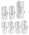
- a field oxide film 2 for element separation is grown on a P type silicon substrate 1 by a well-known LOCOS (Local Oxidation of Silicon) method, and then a gate oxide film 3 is formed by thermal oxidation.
- LOCOS Local Oxidation of Silicon
- the gate oxide film 3 in a predetermined area is etched away as shown in Figure 5C (this forms a predetermined contact part 4).
- a polysilicon layer 5 is deposited on the entire face including the contact part 4 by a well-known CVD (Chemical Vapor Deposition) method; and the polysilicon layer 5 is doped by, for example, phosphorus or the like to be N type; and then after a predetermined area is covered by a photoresist 40, a pattern is defined by, for example, a dry etching in order to leave only a predetermined polysilicon layer 5a (wiring layer) and 5b (gate electrode) as shown in Figure 5E. At this time, the P type silicon substrate 1 is also etched by patterning to form a recessed part 4a as shown in the figure.
- CVD Chemical Vapor Deposition
- the recessed part 4a in the figure is exaggerated to facilitate the understanding as said in the above.
- 4b in the figure is a connecting region of the polysilicon layer 5a and the P type silicon substrate 1 (that is, an N + type diffusion region which will be described later).
- the gate oxide film 3 in a predetermined region is etched away except directly below the polysilicon layer 5b, using the above photoresist 40.
- a predetermined area is selectively ion implanted with an N type impurity (for example As) 50 and is annealed (thermal treatment) to form N + type diffusion region 6 and 7 (source region and drain region) as shown in Figure 5G; and furthermore, an interlevel insulating layer 8 (a phosphorus glass film such as, for example, PSG (Phosphosilicate Glass) or BPSG (Borophosphosilicate Glass)) is deposited as shown in Figure 5H.
- N type impurity for example As
- BPSG Biophosphosilicate Glass
- a purpose of the invention is to provide semiconductor devices which are highly reliable and permit high degree of integration, and a fabrication method thereof.
- Figures 1 - 3 show an embodiment in which the invention is applied to a static RAM.
- N + type source region 6 and an N + type drain region 7 are formed in a predetermined pattern in a major surface of a P type silicon substrate 1; a gate electrode 5b is provided therebetween through a gate oxide film 3; and an N channel MOS transistor (for example, a transistor Q 4 in Figure 2) is structured.
- a wiring layer 5a of a predetermined pattern (for example, this wiring layer 5a is connected to a gate of an N channel MOS transistor Q 1 in Figure 2) is formed on the gate oxide film 3 and a field oxide film 2 formed on the P type silicon substrate 1; an N + type diffusion region 10 is formed by self-diffusion under a contact hole 9 formed in an adjacent region 12 of the wiring layer 5a; and this N + type diffusion region 10 is connected to the source region 6.
- a polysilicon layer 11 (conductive layer) is deposited into the contact hole 9, in a state of connection to the wiring layer 5a. 13 in the figure is a groove.
- Figure 2 is an equivalent circuit diagram showing an example of the static MOS memory.
- Q 1 - Q 6 in Figure 2 are N channel MOS transistors respectively.
- a device of the invention includes the wiring layer 5a of the predetermined pattern formed through the gate oxide film 3, the N + type diffusion layer formed under the contact hole 9 formed in the gate oxide film 3 in the adjacent region 12 of the wiring layer 5a, and the polysilicon layer 11 deposited into the contact hole 9 in a state of connection to the wiring layer 5a, so that the area of a region (the gate oxide film 3 under the wiring layer 5a and the adjacent region 12 of the wiring layer 5a in Figure 1), which corresponds to the contact part 4 (the connecting region 4b and a region of the recess part 4a) in a device by the conventional direct contact method as shown in Figure 5, can be reduced.
- the connection characteristic may be sufficiently secured in this part. Therefore, the gate oxide film 3 under the wiring layer 5a may be smaller (however, this gate oxide film 3 may not entirely removed), so that the area of the above wiring layer 5a and the gate oxide film 3 may be reduced. Also, because the connection to the N + type diffusion region (source region) 6 is made by the self-diffusion of the polysilicon layer 11 buried in the contact hole 9 (that is, by the N + type diffusion region 10), there is little need to consider an excess area by, for example, alignment difference or the like, which is very advantageous to reduction of the device size. Thus, the defects in the direct contact method may be solved, and the high degree of integration of the device is made possible, taking advantage of its characteristic.
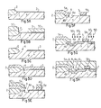
- a field oxide film 2 (for example, 8000 ⁇ thick) is grown on a P type silicon substrate 1 by a well-known LOCOS method, and then a gate oxide film 3 (for example, 200 ⁇ thick) is formed on the silicon substrate 1 by thermal oxidation.
- a polysilicon layer 5 (for example 5000 ⁇ thick) is deposited over the entire face by a well-known, for example, low pressure CVD method; then phosphorus, for example, is deposited by a CVD method at 950 degrees centigrade; and a thermal treatment is performed to dope the polysilicon layer 5 to be an N type.
- a predetermined pattern is defined by, for example, dry etching to form a wiring layer 5a and a gate electrode 5b.
- ion 60 of an N type impurity (for example As) is selectively implanted by a well-known ion implantation method, and an annealing is performed at 950 degrees centigrade to form the N + type diffusion region 6 and 7 (source region and drain region).
- an interlevel insulating layer 8 (for example, BPSG or the like) is deposited over the entire face by, for example, a normal pressure CVD method, and a steam treatment is performed at 850 degrees centigrade to planarize the interlevel insulating layer 8 and to increase the degree of oxidation (insulation).
- a predetermined area is covered with a mask (for example, photoresist, not shown); then a groove 13 is formed by, for example, a dry etching of the interlevel insulating layer 8 in a predetermined area; and a contact hole 9 is formed by etching away the polysilicon layer 5a and removing the gate oxide film 3 by a predetermined dry etching as shown in Figure 3G.
- a mask for example, photoresist, not shown
- a polysilicon layer 11 is deposited by a well-known decreased pressure CVD method over the entire face which includes the contact hole 9 and the groove 13, and the polysilicon layer 11 is made low resistance by annealing at 900 degrees centigrade.
- an N + type diffusion region 10 is formed by self-diffusion under the contact hole 9 to be connected to the source region 6. This connects the polysilicon layer 11 and the wiring layer 5a.
- one process may be omitted by performing the deposition of the polysilicon layer 11 and the anneal at the same step, which is advantageous.
- a layer of SiO 2 (for example, 3000 ⁇ thick) is again deposited by, for example, a well-known decreased pressure CVD method, and each normal wiring treatment is performed to complete the device.
- the device of the embodiment and the fabrication method thereof do not require a mask process which removes the gate oxide film 3 in the predetermined region as in the conventional direct contact method shown in Figure 5B, the reliability of the device may be secured without contamination of the gate oxide film 3. Also, because a cleaning process for the contaminated gate oxide film 3 is not required as in conventional processes, it is an advantageous process without increased number of steps.
- the P type silicon substrate 1 would not be exposed by alignment difference of the mask or the like as in the patterning of the polysilicon layer 5 shown in Figure 5E (because of the gate oxide film 3 as shown in Figure 3C), the P type silicon substrate 1 would not be also etched by a dry etching or the like (because the gate oxide film 3 works as a mask in patterning the polysilicon layer 5). Therefore, it is advantageous for the reliability of the device.
- Figure 4 shows another embodiment of the invention, for instance, an embodiment structured as a diffusion resistance element.
- the same reference numbers are used for the places corresponding to Figure 1.
- the embodiment is basically structured quite similar to the one in Figure 1, but the difference is that it is structured to have, for example, an N + type diffusion region 10 connected to an N + type diffusion region 6 (the source region in the embodiment in Figure 1) in the region where the gate electrode 5b and the drain region 7 are formed in Figure 1 (the region in the right side of Figure 1). That is, the gate electrode as in the above embodiment of Figure 1 does not exist; the above structure is provided symmetrically with the N + type diffusion region 6 in-between; the two diffusion regions 10 are each connected to the N + type diffusion region 6; and the diffusion resistance is formed there.
- an N + type diffusion region 10 connected to an N + type diffusion region 6 (the source region in the embodiment in Figure 1) in the region where the gate electrode 5b and the drain region 7 are formed in Figure 1 (the region in the right side of Figure 1). That is, the gate electrode as in the above embodiment of Figure 1 does not exist; the above structure is provided symmetrically with the N + type diffusion region 6 in-between; the two diffusion regions 10 are each connected to the N +
- 21 in the figure are electrodes to take out the wiring layer 5a; 22 are through holes; and 23 is a SiO 2 layer.
- the device of the embodiment has the similar structure as in the above embodiment of Figure 1, it has the same advantage as in the above embodiment, and it is also structurally convenient for electrical testing.
- a direct contact structure of the invention may be easily checked by using the two diffusion regions 10 and the diffusion region 6 connected thereto shown in the figure as a diffusion resistance and measuring the electric characteristics thereof.
- Resistive valve of 30 - 50 ohm per 1 contact hole may be actually freely controlled, and also very good contact characteristic may be obtained.
- the conductive layer 11 deposited into the contact hole 9 in the above embodiments
- other metal such as Al or the like may be deposited (in this case, metal or the like is deposited after the diffusion layer 10 is previously formed by an impurity diffusion by a conventional art).
- the deposition of the conductive layer (polysilicon layer) 11 and the formation of the diffusion layer 10 by annealing may be performed at the same time.
- the conductive layer 11 may be deposited after the formation of the diffusion layer 10.
- the diffusion may be performed by an adequate optical excitation treatment such as laser anneal, lamp anneal, or the like.
- the invention is applied to, for example, the N channel MOS transistor Q 4 and Q 1 within broken lines in Figure 2 in the above embodiments (that is, it is used for connecting the source of the transistor Q 4 and the gate of the transistor Q1), it may also be applied for connecting the drain of the transistor Q 5 and the gate of the transistor Q 2 , and connecting the source of the transistor Q 4 and the drain of the transistor Q 2 , and so on, in the same figure.
- the invention may be applied to appropriate places in other devices.
- the conductivity types of the each above semiconductor region may be reversed, and the invention may be applied to the appropriate other than static RAMs, for example dynamic RAMs or the like.
- the invention comprises: a wiring layer with a predetermined pattern formed over a major surface of a semiconductor substrate through an insulating film, a diffusion layer formed under a contact hole formed in said insulation film in an adjacent region of the wiring layer, and a conductive layer deposited into said contact hole in a state of being connected to said wiring layer, are occupied by said insulating film and wiring layer and also area of the adjacent region of said wiring layer may be reduced, which allows high degree of integration.
- the contact hole is formed after patterning of the wiring layer over said insulating film, a process of etching said insulating film may be performed without contamination or the like of said insulating film.
Landscapes
- Internal Circuitry In Semiconductor Integrated Circuit Devices (AREA)
- Electrodes Of Semiconductors (AREA)
- Semiconductor Memories (AREA)
Claims (7)
- Verfahren zum Herstellen eines Halbleiterbauelements, umfassend:es wird ein einen Leitfähigkeitstyp aufweisendes Halbleitersubstrat (1), das eine obere Fläche besitzt, vorgesehen,es wird wenigstens ein mit einem Dotierstoff des anderen Leitfähigkeitstyps dotierter Bereich (6) in dem den einen Leitfähigkeitstyp aufweisenden Halbleitersubstrat gebildet, der zu der oberen Fläche des Substrats hinläuft,es wird eine Isolationsschicht (3) auf der oberen Fläche des den einen Leitfähigkeitstyp aufweisenden Halbleitersubstrats so gebildet, daß sie einen relativ dicken Isolationsbereich (2) und einen daran angrenzenden relativ dünnen Isolationsbereich (3) umfaßt,es wird eine aus einem elektrisch leitfähigen Material bestehende Leitungsschicht (5a) über der Isolationsschicht gebildet,die aus elektrisch leitfähigem Material bestehende Leitungsschicht wird strukturiert, um einen Teil des relativ dünnen Isolationsbereichs (3) der darunterliegenden Isolationsschicht freizulegen,es wird eine schichtenübergreifende Isolationsschicht (8) über der strukturierten Leitungsschicht (5a) und der vorher gebildeten Isolationsschicht (3) gebildet,es wird ein Kontaktloch (9) hergestellt, das durch die schichtenübergreifende Isolationsschicht (8), die strukturierte Leitungsschicht (5a) und die Isolationsschicht (3) hindurchläuft undes wird in dem Kontaktloch ein elektrisch leitfähiges Kontaktelement (11) hergestellt, das aus einem Material besteht, das mit einem den anderen Leitfähigkeitstyp aufweisenden Dotierstoff dotiert ist, und das so an der strukturierten Leitungsschicht angreift, daß das elektrisch leitfähige Kontaktelement (11) das Kontaktloch ausfüllt und sich durch die schichtenübergreifende Isolationsschicht (8) und den relativ dünnen Isolationsbereich der Isolationsschicht hindurch erstreckt, bis es an der oberen Fläche des den einen Leitfähigkeitstyp aufweisenden Halbleitersubstrats und dem einen, den anderen Leitfähigkeitstyp aufweisenden dotierten Bereich angreift;dadurch gekennzeichnet, daßdie Bildung des wenigstens einen, den anderen Leitfähigkeitstyp aufweisenden dotierten Bereiches (6) in dem den einen Leitfähigkeitstyp aufweisenden Halbleitersubstrat nach der Bildung der Isolationsschicht auf der oberen Fläche des den einen Leitfähigkeitstyp aufweisenden Halbleitersubstrats und der Bildung und dem Strukturieren der aus elektrisch leitfähigem Material bestehenden Schicht über der Isolationsschicht erfolgt, und durch den Teil des relativ dünnen Isolationsbereiches der Isolationsschicht hindurch erfolgt, der beim Definieren der aus elektrisch leitfähigem Material bestehenden Schicht durch das Strukturieren der aus elektrisch leitfähigem Material bestehenden Schicht freigelegt wurde, so daß die strukturierte, aus elektrisch leitfähigem Material bestehende Leitungsschicht mit dem wenigstens einen, den anderen Leitfähigkeitstyp aufweisenden dotierten Bereich in Ausrichtung gebracht wird,das Kontakt loch durch Entfernen eines Teils der strukturierten Leitungsschicht (5a) und eines entsprechenden Teils des relativ dünnen Isolationsbereichs (3) der darunterliegenden Isolationsschicht gebildet wird, um die obere Fläche des den einen Leitfähigkeitstyp aufweisenden Halbleitersubstrats und des einen dotierten Bereichs freizulegen, wobei das Kontaktloch so liegt, daß der eine, den anderen Leitfähigkeitstyp aufweisende dotierte Bereich, der zu der oberen Fläche des den einen Leitfähigkeitstyp aufweisenden Substrats führt, teilweise freigelegt wird, während außerdem ein Teil der oberen Fläche des den einen Leitfähigkeitstyp aufweisenden Halbleitersubstrats freigelegt wird, undden anderen Leitfähigkeitstyp aufweisender Dotierstoff von dem in dem Kontaktloch gebildeten, elektrisch leitfähigen Kontaktelement in das den einen Leitfähigkeitstyp aufweisende Halbleitersubstrat diffundiert, so daß ein den anderen Leitfähigkeitstyp aufweisender dotierter Bereich (10) gebildet wird, der sich über das Kontaktloch spannt und sich über das den einen Leitfähigkeitstyp aufweisende Halbleitersubstrat erstreckt, um in den den anderen Leitfähigkeitstyp aufweisenden dotierten Bereich einzumünden, so daß die elektrische Verbindung zwischen dem Kontaktelement und dem den anderen Leitfähigkeitstyp aufweisenden dotierten Bereich zumindest verbessert wird.
- Verfahren zum Herstellen eines Halbleiterbauelements nach Anspruch 1, darüber hinaus dadurch gekennzeichnet, daß die Bildung des wenigstens einen, den anderen Leitfähigkeitstyp aufweisenden dotierten Bereichs (6) durch selektive Ionenimplantation des den anderen Leitfähigkeitstyp aufweisenden Dotierstoffs in das den einen Leitfähigkeitstyp aufweisende Halbleitersubstrat erzielt wird.
- Verfahren zum Herstellen eines Halbleiterbauelements nach einem der Ansprüche 1 bis 2 , darüber hinaus dadurch gekennzeichnet, daßdie Leitungsschicht über der Isolationsschicht gebildet wird, indem eine Schicht aus polykristallinem Halbleitermaterial über der Isolationsschicht abgeschieden wird,die Schicht aus polykristallinem Halbleitermaterial mit einem den anderen Leitfähigkeitstyp aufweisenden Dotierstoff versehen wird, unddie aus elektrisch leitfähigem Material bestehende Leitungsschicht definiert wird, indem die Schicht aus polykristallinem Halbleitermaterial strukturiert wird.
- Verfahren zum Herstellen eines Halbleiterbauelements nach Anspruch 3, darüber hinaus dadurch gekennzeichnet, daßdas Kontaktelement in dem Kontaktloch durch Abscheiden einer zweiten Schicht aus polykristallinem Halbleitermaterial über der Isolationsschicht gebildet wird und das es das sich dadurch erstreckende Kontaktloch ausfüllt,die zweite Schicht aus polykristallinem Halbleitermaterial mit einem den anderen Leitfähigkeitstyp aufweisenden Dotierstoff versehen wird unddas aus elektrisch leitfähigem Material bestehende Kontaktelement definiert wird, indem die gesamte zweite, aus polykristallinem Halbleitermaterial bestehende Schicht, mit Ausnahme des Teils innerhalb des Kontaktlochs, entfernt wird.
- Verfahren zum Herstellen eines Halbleiterbauelements nach Anspruch 4, darüber hinaus dadurch gekennzeichnet, daßdie zweite Schicht aus polykristallinem Halbleitermaterial einem Ausheizprozeß ausgesetzt wird, um ihren elektrischen Widerstand so weit zu vermindern, daß das Material elektrisch leitfähig wird, unddanach das aus elektrisch leitfähigem Material bestehende Kontaktelement definiert wird, indem die gesamte ausgeheizte zweite, aus polykristallinem Halbleitermaterial bestehende Schicht, mit Ausnahme des Teils innerhalb des Kontaktlochs, entfernt wird.
- Verfahren zum Herstellen eines Halbleiterbauelements nach Anspruch 5, darüber hinaus dadurch gekennzeichnet, daß die Diffusion des den anderen Leitfähigkeitstyp aufweisenden Dotierstoffs von dem elektrisch leitfähigen Kontaktelement in das den einen Leitfähigkeitstyp aufweisende Halbleitersubstrat als Reaktion auf den Ausheizprozeß der zweiten Schicht aus polykristallinem Halbleitermaterial auftritt.
- Verfahren zum Herstellen eines Halbleiterbauelements nach einem der Ansprüche 1 bis 6, darüber hinaus dadurch gekennzeichnet, daßwährend des Schritts des Strukturierens der aus elektrisch leitfähigem Material bestehenden Leitungsschicht eine Gateelektrode (5b) gebildet wird, die auf dem relativ dünnen Isolationsbereich (3) der Isolationsschicht angeordnet ist und über einem Teil des den einen Leitfähigkeitstyp aufweisenden Halbleitersubstrats (1) liegt ist,während des Schritts des Bildens wenigstens eines dotierten Bereichs ein Paar von beabstandeten, den anderen Leitfähigkeitstyp aufweisenden dotierten Bereichen (6, 7) in dem den einen Leitfähigkeitstyp aufweisenden Substrat gebildet wird, die in Ausrichtung mit der Gateelektrode zu der oberen Fläche des Halbleitersubstrats hinlaufen, wobei das Paar der den anderen Leitfähigkeitstyp aufweisenden dotierten Bereiche jeweils aus einem Sourcebereich und einem Drainbereich besteht,das elektrisch leitfähige Kontaktelement, dessen Material mit einem den anderen Leitfähigkeitstyp aufweisenden Dotierstoff dotiert ist, in dem Kontaktloch so hergestellt wird, daß es an der strukturierten Leitungsschicht und an einem der den anderen Leitfähigkeitstyp aufweisenden Bereiche des aus dem Source- und dem Drainbereich gebildeten Paares angreift und in Abstand zu der Gateelektrode angeordnet ist, undder den anderen Leitfähigkeitstyp aufweisende Dotierstoff von dem elektrisch leitfähigen Element in das den einen Leitfähigkeitstyp aufweisende Halbleitersubstrat diffundiert, wodurch der diffundierte, den anderen Leitfähigkeitstyp aufweisende dotierte Bereich definiert wird, der sich über das Kontakt loch spannt und sich über das den einen Leitfähigkeitstyp aufweisende Halbleitersubstrat erstreckt, um in den einen der den anderen Leitfähigkeitstyp aufweisenden Bereiche des aus dem Source- und dem Drainbereich gebildeten Paares einzumünden, so daß die elektrische Verbindung zwischen dem Kontaktelement und dem einen den anderen Leitfähigkeitstyp aufweisenden Bereich des aus dem Source- und dem Drainbereich gebildeten Paares zumindest verbessert wird.
Applications Claiming Priority (2)
| Application Number | Priority Date | Filing Date | Title |
|---|---|---|---|
| JP21807/89 | 1989-01-31 | ||
| JP1021807A JPH02202054A (ja) | 1989-01-31 | 1989-01-31 | 半導体装置及びその製造方法 |
Publications (3)
| Publication Number | Publication Date |
|---|---|
| EP0380964A2 EP0380964A2 (de) | 1990-08-08 |
| EP0380964A3 EP0380964A3 (de) | 1991-03-13 |
| EP0380964B1 true EP0380964B1 (de) | 1997-05-21 |
Family
ID=12065325
Family Applications (1)
| Application Number | Title | Priority Date | Filing Date |
|---|---|---|---|
| EP90100909A Expired - Lifetime EP0380964B1 (de) | 1989-01-31 | 1990-01-17 | Verfahren zur Herstellung eines Halbleiterbauelements mit einem Kontaktteil |
Country Status (3)
| Country | Link |
|---|---|
| EP (1) | EP0380964B1 (de) |
| JP (1) | JPH02202054A (de) |
| DE (1) | DE69030743T2 (de) |
Families Citing this family (2)
| Publication number | Priority date | Publication date | Assignee | Title |
|---|---|---|---|---|
| GB9219268D0 (en) * | 1992-09-11 | 1992-10-28 | Inmos Ltd | Semiconductor device incorporating a contact and manufacture thereof |
| JP3256048B2 (ja) * | 1993-09-20 | 2002-02-12 | 富士通株式会社 | 半導体装置及びその製造方法 |
Family Cites Families (2)
| Publication number | Priority date | Publication date | Assignee | Title |
|---|---|---|---|---|
| JPS59220952A (ja) * | 1983-05-31 | 1984-12-12 | Toshiba Corp | 半導体装置の製造方法 |
| ES2046209T3 (es) * | 1986-12-17 | 1995-04-01 | Advanced Micro Devices Inc | Estructura de contacto a tope de area reducida. |
-
1989
- 1989-01-31 JP JP1021807A patent/JPH02202054A/ja active Pending
-
1990
- 1990-01-17 DE DE69030743T patent/DE69030743T2/de not_active Expired - Fee Related
- 1990-01-17 EP EP90100909A patent/EP0380964B1/de not_active Expired - Lifetime
Non-Patent Citations (1)
| Title |
|---|
| "VLSI Technology", S.M.Sze, 1983, pages 169-171 * |
Also Published As
| Publication number | Publication date |
|---|---|
| JPH02202054A (ja) | 1990-08-10 |
| EP0380964A2 (de) | 1990-08-08 |
| DE69030743D1 (de) | 1997-06-26 |
| EP0380964A3 (de) | 1991-03-13 |
| DE69030743T2 (de) | 1997-11-13 |
Similar Documents
| Publication | Publication Date | Title |
|---|---|---|
| US5385857A (en) | Method of manufacturing a semiconductor device with high packing density and having field effect transistors | |
| KR900000207B1 (ko) | 반도체 기억장치와 그 제조방법 | |
| US4466172A (en) | Method for fabricating MOS device with self-aligned contacts | |
| KR0144906B1 (ko) | 불휘발성 메모리 소자 및 그 제조방법 | |
| US5061651A (en) | Method of making dram cell with stacked capacitor | |
| US4984055A (en) | Semiconductor device having a plurality of conductive layers and manufacturing method therefor | |
| US4849854A (en) | Semiconductor device and method of manufacturing the same | |
| US4446613A (en) | Integrated circuit resistor and method of fabrication | |
| US5091768A (en) | Semiconductor device having a funnel shaped inter-level connection | |
| US5627095A (en) | Method for fabricating semiconductor devices having bit lines and storage node contacts | |
| US5043298A (en) | Process for manufacturing a DRAM cell | |
| JP4550185B2 (ja) | Dram装置の製造方法 | |
| US6426528B2 (en) | Method of fabricating conductive straps to interconnect contacts to corresponding digit lines by employing an angled sidewall implant and semiconductor devices fabricated thereby | |
| KR930009016B1 (ko) | 반도체장치의 배선접촉구조 및 그 제조방법 | |
| JP3897934B2 (ja) | 半導体装置のコンタクトホール製造方法 | |
| US6040221A (en) | Semiconductor processing methods of forming a buried contact, a conductive line, an electrical connection to a buried contact area, and a field effect transistor gate | |
| US4616402A (en) | Method of manufacturing a semiconductor device with a stacked-gate-electrode structure | |
| EP0160965B1 (de) | Verfahren zum Herstellen einer Halbleiteranordnung mit einer Gateelektrodenstapel-Struktur | |
| US5243219A (en) | Semiconductor device having impurity diffusion region formed in substrate beneath interlayer contact hole | |
| US6825112B2 (en) | Semiconductor device and method of production thereof | |
| EP0380964B1 (de) | Verfahren zur Herstellung eines Halbleiterbauelements mit einem Kontaktteil | |
| US5221634A (en) | Method of making semiconductor device employing self diffusion of dopant from contact member for augmenting electrical connection to doped region in substrate | |
| US7332811B2 (en) | Integrated circuit interconnect | |
| US6261940B1 (en) | Semiconductor method of making electrical connection between an electrically conductive line and a node location, and integrated circuitry | |
| KR100200697B1 (ko) | 가드링을 구비하는 반도체장치 및 이를 이용한 콘택트 형성방법 |
Legal Events
| Date | Code | Title | Description |
|---|---|---|---|
| PUAI | Public reference made under article 153(3) epc to a published international application that has entered the european phase |
Free format text: ORIGINAL CODE: 0009012 |
|
| AK | Designated contracting states |
Kind code of ref document: A2 Designated state(s): DE FR GB IT NL |
|
| PUAL | Search report despatched |
Free format text: ORIGINAL CODE: 0009013 |
|
| AK | Designated contracting states |
Kind code of ref document: A3 Designated state(s): DE FR GB IT NL |
|
| 17P | Request for examination filed |
Effective date: 19910910 |
|
| 17Q | First examination report despatched |
Effective date: 19940210 |
|
| GRAG | Despatch of communication of intention to grant |
Free format text: ORIGINAL CODE: EPIDOS AGRA |
|
| GRAH | Despatch of communication of intention to grant a patent |
Free format text: ORIGINAL CODE: EPIDOS IGRA |
|
| GRAH | Despatch of communication of intention to grant a patent |
Free format text: ORIGINAL CODE: EPIDOS IGRA |
|
| GRAA | (expected) grant |
Free format text: ORIGINAL CODE: 0009210 |
|
| ITF | It: translation for a ep patent filed | ||
| AK | Designated contracting states |
Kind code of ref document: B1 Designated state(s): DE FR GB IT NL |
|
| PG25 | Lapsed in a contracting state [announced via postgrant information from national office to epo] |
Ref country code: NL Free format text: LAPSE BECAUSE OF FAILURE TO SUBMIT A TRANSLATION OF THE DESCRIPTION OR TO PAY THE FEE WITHIN THE PRESCRIBED TIME-LIMIT Effective date: 19970521 |
|
| REF | Corresponds to: |
Ref document number: 69030743 Country of ref document: DE Date of ref document: 19970626 |
|
| ET | Fr: translation filed | ||
| NLV1 | Nl: lapsed or annulled due to failure to fulfill the requirements of art. 29p and 29m of the patents act | ||
| PLBE | No opposition filed within time limit |
Free format text: ORIGINAL CODE: 0009261 |
|
| STAA | Information on the status of an ep patent application or granted ep patent |
Free format text: STATUS: NO OPPOSITION FILED WITHIN TIME LIMIT |
|
| 26N | No opposition filed | ||
| REG | Reference to a national code |
Ref country code: GB Ref legal event code: IF02 |
|
| PGFP | Annual fee paid to national office [announced via postgrant information from national office to epo] |
Ref country code: GB Payment date: 20061213 Year of fee payment: 18 |
|
| PGFP | Annual fee paid to national office [announced via postgrant information from national office to epo] |
Ref country code: DE Payment date: 20070131 Year of fee payment: 18 |
|
| PGFP | Annual fee paid to national office [announced via postgrant information from national office to epo] |
Ref country code: IT Payment date: 20070627 Year of fee payment: 18 |
|
| PGFP | Annual fee paid to national office [announced via postgrant information from national office to epo] |
Ref country code: FR Payment date: 20070103 Year of fee payment: 18 |
|
| GBPC | Gb: european patent ceased through non-payment of renewal fee |
Effective date: 20080117 |
|
| PG25 | Lapsed in a contracting state [announced via postgrant information from national office to epo] |
Ref country code: DE Free format text: LAPSE BECAUSE OF NON-PAYMENT OF DUE FEES Effective date: 20080801 |
|
| REG | Reference to a national code |
Ref country code: FR Ref legal event code: ST Effective date: 20081029 |
|
| PG25 | Lapsed in a contracting state [announced via postgrant information from national office to epo] |
Ref country code: GB Free format text: LAPSE BECAUSE OF NON-PAYMENT OF DUE FEES Effective date: 20080117 |
|
| PG25 | Lapsed in a contracting state [announced via postgrant information from national office to epo] |
Ref country code: FR Free format text: LAPSE BECAUSE OF NON-PAYMENT OF DUE FEES Effective date: 20080131 |
|
| PG25 | Lapsed in a contracting state [announced via postgrant information from national office to epo] |
Ref country code: IT Free format text: LAPSE BECAUSE OF NON-PAYMENT OF DUE FEES Effective date: 20080117 |