EP0380983A2 - Commutateur à semi-conducteur optique et réseau avec de tels commutateurs - Google Patents
Commutateur à semi-conducteur optique et réseau avec de tels commutateurs Download PDFInfo
- Publication number
- EP0380983A2 EP0380983A2 EP90101120A EP90101120A EP0380983A2 EP 0380983 A2 EP0380983 A2 EP 0380983A2 EP 90101120 A EP90101120 A EP 90101120A EP 90101120 A EP90101120 A EP 90101120A EP 0380983 A2 EP0380983 A2 EP 0380983A2
- Authority
- EP
- European Patent Office
- Prior art keywords
- light wave
- waveguide
- switch
- set forth
- optical switch
- Prior art date
- Legal status (The legal status is an assumption and is not a legal conclusion. Google has not performed a legal analysis and makes no representation as to the accuracy of the status listed.)
- Granted
Links
Images


Classifications
-
- G—PHYSICS
- G02—OPTICS
- G02F—OPTICAL DEVICES OR ARRANGEMENTS FOR THE CONTROL OF LIGHT BY MODIFICATION OF THE OPTICAL PROPERTIES OF THE MEDIA OF THE ELEMENTS INVOLVED THEREIN; NON-LINEAR OPTICS; FREQUENCY-CHANGING OF LIGHT; OPTICAL LOGIC ELEMENTS; OPTICAL ANALOGUE/DIGITAL CONVERTERS
- G02F1/00—Devices or arrangements for the control of the intensity, colour, phase, polarisation or direction of light arriving from an independent light source, e.g. switching, gating or modulating; Non-linear optics
- G02F1/29—Devices or arrangements for the control of the intensity, colour, phase, polarisation or direction of light arriving from an independent light source, e.g. switching, gating or modulating; Non-linear optics for the control of the position or the direction of light beams, i.e. deflection
- G02F1/31—Digital deflection, i.e. optical switching
- G02F1/313—Digital deflection, i.e. optical switching in an optical waveguide structure
- G02F1/3137—Digital deflection, i.e. optical switching in an optical waveguide structure with intersecting or branching waveguides, e.g. X-switches and Y-junctions
- G02F1/3138—Digital deflection, i.e. optical switching in an optical waveguide structure with intersecting or branching waveguides, e.g. X-switches and Y-junctions the optical waveguides being made of semiconducting materials
-
- H—ELECTRICITY
- H01—ELECTRIC ELEMENTS
- H01S—DEVICES USING THE PROCESS OF LIGHT AMPLIFICATION BY STIMULATED EMISSION OF RADIATION [LASER] TO AMPLIFY OR GENERATE LIGHT; DEVICES USING STIMULATED EMISSION OF ELECTROMAGNETIC RADIATION IN WAVE RANGES OTHER THAN OPTICAL
- H01S5/00—Semiconductor lasers
- H01S5/50—Amplifier structures not provided for in groups H01S5/02 - H01S5/30
-
- H—ELECTRICITY
- H04—ELECTRIC COMMUNICATION TECHNIQUE
- H04Q—SELECTING
- H04Q11/00—Selecting arrangements for multiplex systems
- H04Q11/0001—Selecting arrangements for multiplex systems using optical switching
- H04Q11/0005—Switch and router aspects
-
- H—ELECTRICITY
- H04—ELECTRIC COMMUNICATION TECHNIQUE
- H04Q—SELECTING
- H04Q11/00—Selecting arrangements for multiplex systems
- H04Q11/0001—Selecting arrangements for multiplex systems using optical switching
- H04Q11/0005—Switch and router aspects
- H04Q2011/0007—Construction
- H04Q2011/0015—Construction using splitting combining
-
- H—ELECTRICITY
- H04—ELECTRIC COMMUNICATION TECHNIQUE
- H04Q—SELECTING
- H04Q11/00—Selecting arrangements for multiplex systems
- H04Q11/0001—Selecting arrangements for multiplex systems using optical switching
- H04Q11/0005—Switch and router aspects
- H04Q2011/0037—Operation
- H04Q2011/0041—Optical control
-
- H—ELECTRICITY
- H04—ELECTRIC COMMUNICATION TECHNIQUE
- H04Q—SELECTING
- H04Q11/00—Selecting arrangements for multiplex systems
- H04Q11/0001—Selecting arrangements for multiplex systems using optical switching
- H04Q11/0005—Switch and router aspects
- H04Q2011/0052—Interconnection of switches
Definitions
- the present invention relates to an optical switch having waveguides. More particularly, the present invention pertains to a semiconductor optical switch which is suitable for use in an optical integrated circuit or opto-electronic integrated circuit employed for optical computing, optical information transmission, etc.
- semiconductor optical switches i.e., a semiconductor waveguide type optical switch which has a short device length and therefore enables large scale integration on a semiconductor substrate, a slip structure type optical switch and an integrated semiconductor waveguide type optical switch which is employed for an photonic switching .
- a semiconductor waveguide type optical switch which has a short device length and therefore enables large scale integration on a semiconductor substrate
- slip structure type optical switch and an integrated semiconductor waveguide type optical switch which is employed for an photonic switching .
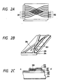
- FIGURE 2A A 4 x 4 optical switch array is shown in FIGURE 2A.
- a plurality of optical waveguides are provided on a semiconductor substrate.
- the plurality of waveguides have a plurality of X-crossing waveguides and are optically coupled to optical fibers 201 on the signal input side and optical fibers 202 on the signal output side.
- An enlarged view of a unit cell of an optical switch that constitues an X-crossing waveguide is shown in FIGURE 2B.
- An additional waveguide is connected to respective parts of waveguides that cross each other in the shape of an X, thus defining two Y-branches 203.
- These waveguides 206 are produced in such a manner that a semiconductor material, for example, inGaAsp, is grown on an InP substrate 204 to provide a layer 205, which is then subjected to, for example, reactive ion-beam etching using Cl2 or the like with a photoresist used as a mask, thereby forming a ridge-shaped structure.
- the sectional area of the ridge waveguides 206 is about 5 ⁇ m width x 1.5 ⁇ m height.
- FIGURE 2C The sectional view of the optical switch shown in FIGURE 2B, taken along the line A-A′, is shown in FIGURE 2C.
- a waveguide layer 205 (bandgap wavelength: 1.15 ⁇ m) of n-InGaAsP, a cladding layer 206 of n-InP and a cap layer 207 of n-InGaAsP by ordinary LPE (Liquid Phase Epitaxy) method.
- LPE Liquid Phase Epitaxy
- n-side electrode 211 is similarly provided on the reverse side of the InP substrate 204.
- This optical switch which utilizes a refractive index change on the basis of carrier injection, is relatively large in the amount of change in the refractive index of the constituent material and therefore suitable, particularly, for fabricating an optical switch array having small-sized optical switches and a large number of light input and output waveguides.
- optical switch or optical switch array involves some propagation losses, for example, increases in the loss and crosstalk caused by scattering of light at the branches and inferior optical switch characteristics, and waveguide loss intrinsic to the waveguides. These propagation losses are technical problems which cannot be ignored when it is intended to integrate optical switches in a large size and at a high density.
- the present invention aims at solving the above-described technical problems of the prior art and relates to an optical switch having novel functions and an optical switch array employing the same.
- a semiconductor optical switch comprising: a first waveguide for guiding a light wave; a second waveguide for guiding the light wave; propagation direction changing means disposed between the first and second waveguides to change the direction of propagation of the light wave propagated through the first waveguide; a third waveguide connecting together the first and second waveguides to guide the light wave from the first waveguide to the second waveguide; and light wave amplifying means provided on the third waveguide to amplify the light wave propagated through the third waveguide.
- a semiconductor laser structure may be employed as the light wave amplifying means.
- Semiconductor lasers have an optically active region.
- the states of the optically active region may be classified into three, that is, lasing state, amplifying state and absorbing state in accordance with the level of the carrier energy injected into the region.
- the present invention positively utilizes the amplifying state or the absorbing state of the three states.
- Such a semiconductor laser structure is optically connected to the third waveguide.
- a semiconductor optical switch is realized by combining the above-described light wave amplifying means with the propagation direction changing means that utilizes a change in the refractive index of a semiconductor medium induced by carrier injection from an electrode.
- the operating timing of the light wave amplifying means and the operating timing of the propagation direction changing means are synchronized with each other.
- This synchronization may be obtained by activating the light wave amplifying means and the propagation direction changing means by use of a common electrode.
- the above-described semiconductor optical switch further comprises a fourth waveguide which is different from the second waveguide for guiding the light wave propagated through the first waveguide.
- the propagation direction changing means propagates the light wave propagated through the first waveguide to either the second or fourth waveguide in response to a signal externally applied to the propagation direction changing means.
- the above-described semiconductor optical switch further comprises a fifth waveguide for guiding a second light wave other than the first light wave propagated through the first waveguide.
- the second waveguide propagates either the first or second light wave by the operation of the propagation direction changing means in response to a signal externally applied to the propagation direction changing means.
- the fifth waveguide is (optically) connected to the propagation direction changing means such that the second light wave propagated through the fifth waveguide will not be propagated through the third waveguide.
- the second waveguide propagates either the first or second light wave in response to a signal externally applied to the propagation direction changing means.
- the light wave amplifying means of the above-described semiconductor optical switch has a monitor function for light wave discrimination.
- a semiconductor optical switch makes it possible to discriminate between the first and second light waves.
- the light wave amplifying means having a monitor function the above-described one that utilizes a semiconductor laser structure may be employed, for example.
- the light wave amplifying means of the semiconductor optical switch is connected with discrimination means for the light wave discrimination.
- the light wave amplifying means of the semiconductor optical switch has a gate function.
- the light wave amplifying means absorbs the first light wave when the first light wave need not be guided to the second waveguide.
- a semiconductor optical switch comprising: a plurality of input waveguides and a plurality of output waveguides; a plurality of switching function portions respectively disposed at the intersections of the input and output waveguides: and a plurality of light wave amplifying means provided in the switching function portions, respectively. Since such a semiconductor optical switch has a light wave amplifying means in each switching function portion, a specific light wave alone is amplified in each switching function portion.
- the switching function portions of the above-described semiconductor optical switch have bypass waveguides which propagate only a light wave propagated through a specific one of the input waveguides, the light wave ampoifying means being respectively provided in the bypass waveguides.
- a semiconductor optical switch which receives a plurality of input light waves, amplifies only a specific input light wave selected from among the input light waves and outputs the amplified input light wave.
- the specific output light wave includes substantially no amplified input light waves other than the specific input light wave.
- a semiconductor optical switch array comprising a combination of a plurality of semiconductor optical switches as set forth above.
- a semiconductor optical switch comprising optical amplifying means provided in a bypass waveguide which is defined by part of the slip of either a single or double slip structure type optical switch.
- the light that is guided through a light wave modulating means is after the modulation, optically amplified at the output end, for example.
- the propagation loss in the light wave modulating means is compensated for by the optical amplification but, at the same time, an unnecessary light wave component that is mixed in the light due to crosstalk or the like in the light wave modulating means is also optically amplified and consequently the noise component in the output light wave does not decrease. It is necessary in order to solve this problem to subject only the required light wave to optical amplification. However, if this optical amplification is conducted before the light reaches the light wave modulating means, the crosstalk of the required light wave increases instead, which similarly results in a lowering in the output margin of the semiconductor optical switch.
- the switching function portion has a portion which selects a specific light wave (in other words, changes the direction of propagation), and if the light wave is optically amplified after passing through this portion, it is possible to amplify only the required light wave.
- the switching function portion specifically, in the output waveguide
- the switching function portion in the present invention is a region which is disposed between an input waveguide and an output waveguide and which has a function for deflecting light.
- the amplification region of a semiconductor laser or the like functions as an absorbing portion when not excited and amplifies when sufficiently excited.
- the third waveguide, or the bypass waveguide that is part of the slip of either a single or double slip structure type optical switch, in the present invention has a function by which only an optical signal to be exchanged passes therethrough, which is not present in any conventional optical switches. Therefore, if an optical amplification function is imparted to this bypass waveguide, it is possible to enable the bypass waveguide to function as an absorbing portion when the optical switch is in an OFF-state (a state wherein no optical signal passes through the bypass waveguide) and function as an amplification portion when the optical switch is in ON-stage (a state wherein an optical signal passes through the bypass waveguide).
- the crosstalk is markedly reduced and consequently the loss is reduced or the optical signal is amplified in accordance with the amplification degree in the amplification portion.
- the amplification degree can be individually adjusted when optical switches of the type described above are integrated in a large scale and it is therefore possible to obtain uniform characteristics of the resulting optical switch array. Since it is also possible to convert the light absorbed in the optical amplification portion into an electrical signal and read it, the optical amplification portion can be used as an optical signal monitor. Accordingly, when the present invention is applied to an optical processing apparatus such as a photonic switching, it is possible to discriminate between cells and judge the end of a call, for example.
- carrier injection can be used for both the switching and amplifying functions and it is therefore possible to readily realize an optical switch having a small size and high function.
- carrier injection can be used for both the switching and amplifying functions and it is therefore possible to readily realize an optical switch having a small size and high function.
- optical switch array for an optical exchange which is small in size and superior in crosstalk characteristics and low-loss characteristics.
- FIGURE 1A is a perspective view of the optical switch, in which a bypass waveguide 101 which has a single slip structure is provided with an optical amplification portion 102.
- FIGURE 1B shows the cross-sectional structure (taken along the line B-B′ of FIGURE 1A) of the bypass waveguide 101.
- waveguides having the cross-sectional configuration shown in FIGUREs 4A and 4B were formed by ordinary lithography and etching techniques, as being waveguides 109 which were out of the amplification portion and as being a waveguide which was in the amplification portion 101.
- the waveguides thus formed had a width of 5 ⁇ m.
- the X-crossing angle of the waveguides was 14°, and the Y-branch angle of the waveguides was 7°.
- the optical switch thus formed was provided with carrier injection regions 110 for an optical switch operation and electrodes 112 for carrier injection into the associated regions by use of ordinary electrode forming technique.
- FIGURE 4C shows the cross-sectional structure of a waveguide including a carrier injection region 110 of the optical switch formed as described above.
- Zn diffusion method was employed.
- Other features of the waveguide structure shown in FIGUREs 4A and 4B are that the junction loss is small since the waveguide layer 104 is common to the amplification portion and the optical switch portion and that the polarization dependence is small since the optical amplification layer 106 amplifies the evanescent component in the guided light.
- the operation of the thus produced optical switch will next be explained with reference to FIGUREs 5 and 6.
- semiconductor laser light having a wavelength of 1.3 ⁇ m was applied to the input end 511.
- the electrodes of the optical switch portion and the amplification portion were connected to provide a common terminal 515 to drive both the carrier injection portions at the same time.
- the output end 512 was substantially completely switched to the output end 513 when the injection current was about 200 mA, and the insertion loss and the crosstalk were 3 dB and -30 dB, respectively, which were 5 dB and 10 dB smaller than those of a device provided with no optical amplification portion.
- the two carrier injection portions were individually driven by use of the arrangement shown in FIGURE 6, that is, by use of terminals 616 and 617 provided in connection with the respective electrodes of the optical switch portion and the optical amplification portion.
- the optical switch portion and the optical amplification portion were supplied with injection currents of about 120 mA and about 200 mA, respectively, the direction of propagation of the light with a wavelength of 1.3 ⁇ m input from the input end 611 was substantially completely changed from the output end 612 to the output end 613.
- the insertion loss and the crosstalk were -2 dB and -30 dB, respectively. That is, it was possible to obtain a gain of 2 dB. As a result, it was possible to confirm the basic functions of the present invention for reducing or eliminating loss and reducing crosstalk.
- FIGURE 3 Although in this embodiment the range structure shown in FIGURE 3 was employed for the waveguides, it is, of course, possible to obtain the same advantageous effects by use of gain type optical waveguide structures in addition to refractive index type optical waveguide structures such as those of loaded type, BH type and CSP type, which are ordinary optical waveguide structures.
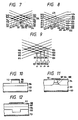
- FIGUREs 10, 11 and 12 respectively shows examples of specific optical waveguide structures of loaded type, BH type and CSP type.
- the reference numeral 114 in FIGURE 11 denotes a buried layer (region) which is a semiconductor (InP or the like) region for confining the light propagated through the waveguide region 104 and the injected current within the mesa region in the center.
- a semiconductor InP or the like
- III-V group semiconductor materials such as GaAlAs, InGaAlAs, etc. and II-VI group semiconductor materials.
- FIGURE 7 one embodiment of the optical switch array according to the present invention will be explained.
- 16 semiconductor optical switches of the type shown in FIGURE 1A were integrated to produce a complete lattice-type 4 x 4 optical switch array having 4 inputs and 4 outputs, as shown in the figure. Since the bypass waveguide that is part of the slip of the single or double slip structure type optical switch according to the present invention has a function by which only an optical signal which is to be exchanged passes therethrough, which is unavailable in the conventional optical switches, it is possible to realize an optical exchange function which is not present in the prior art.
- the output ends 831, 832, 833 and 834 to which optical signals input from the input ends 811, 812, 813 and 814 are to be output depend on which ones of the switch units disposed at the lattice points in the optical switch array turn ON, and since the path, length, etc. of the waveguides differ depending upon each particular connecting condition, if the optical amplifiers 821, 822, 823 and 824 disposed at the input or output ends are operated under a constant condition, it is impossible to adjust variations in loss due to the connecting condition.
- optical signals from the input ends 811, 812, 813 and 814 are output to the output end 831 when the switch units 411, 421, 431 and 441 turn on, respectively. Since the length and condition of the waveguides differ for each path, the loss value differs for each path, as a matter of course.
- the optical switch array shown in FIGURE 7 that comprises semiconductor optical switches of the present invention enables adjustment loss variations due to the difference in path, length, etc. of the waveguides depending upon the connecting condition since a switch unit disposed at each lattice point has each individual optical amplification function.
- the path from an input end to an output end is uniformly determined by which one(s) of the switch units at the lattice points turn ON, it suffices to unconditionally determine an amplification degree at each lattice point in accordance with the loss in this path.
- the optical amplification degrees of four switch units 311, 312, 313 and 314 in the arrangement shown in FIGURE 7 were individually adjusted so that the optical signal input from the input end 711 was output to the output ends 731, 732, 733 and 734 with the same light intensity and so that the insertion loss was 5 dB.
- the values of the current required were 200, 220, 230 and 260 mA, respectively.
- the optical amplification degrees of the remaining 12 switch units 321, 322, 323, 324, 331, 332, 333, 334, 341, 342, 343 and 344 were individually adjusted so that the optical signals input from the input ends 712, 713 and 714 were output to the output ends 731, 732, 733 and 734 with the same light intensity and so that the insertion loss was 5 dB.
- an optical signal input from any input end is output to any output end with the same light intensity.
- FIGURE 9 one embodiment of an optical exchange that utilizes the optical signal monitor function of the present invention will be explained.
- An optical signal input from the input end 911 was monitored on the basis of a change in the terminal voltage in the optical amplification portion of each of the switch units 311, 312, 313 and 314 (in the figure, the reference numerals 921 to 924 denote optical switch unit driving power supplies having a voltage monitor circuit and therefore serving also as monitor means), thereby reading the header portion in the optical signal to discriminate an output end to be connected from the others.
- the corresponding switch unit 312 was turned ON so that the signal would be output to the corresponding output end 932.
Landscapes
- Physics & Mathematics (AREA)
- Nonlinear Science (AREA)
- General Physics & Mathematics (AREA)
- Optics & Photonics (AREA)
- Condensed Matter Physics & Semiconductors (AREA)
- Electromagnetism (AREA)
- Engineering & Computer Science (AREA)
- Computer Networks & Wireless Communication (AREA)
- Optical Integrated Circuits (AREA)
- Optical Modulation, Optical Deflection, Nonlinear Optics, Optical Demodulation, Optical Logic Elements (AREA)
- Semiconductor Lasers (AREA)
Applications Claiming Priority (2)
| Application Number | Priority Date | Filing Date | Title |
|---|---|---|---|
| JP17604/89 | 1989-01-30 | ||
| JP1017604A JP2656598B2 (ja) | 1989-01-30 | 1989-01-30 | 半導体光スイッチ及び半導体光スイッチアレイ |
Publications (3)
| Publication Number | Publication Date |
|---|---|
| EP0380983A2 true EP0380983A2 (fr) | 1990-08-08 |
| EP0380983A3 EP0380983A3 (fr) | 1991-06-19 |
| EP0380983B1 EP0380983B1 (fr) | 1995-09-13 |
Family
ID=11948486
Family Applications (1)
| Application Number | Title | Priority Date | Filing Date |
|---|---|---|---|
| EP90101120A Expired - Lifetime EP0380983B1 (fr) | 1989-01-30 | 1990-01-19 | Commutateur à semi-conducteur optique et réseau avec de tels commutateurs |
Country Status (5)
| Country | Link |
|---|---|
| US (2) | US5044745A (fr) |
| EP (1) | EP0380983B1 (fr) |
| JP (1) | JP2656598B2 (fr) |
| CA (1) | CA2007747C (fr) |
| DE (1) | DE69022257T2 (fr) |
Cited By (4)
| Publication number | Priority date | Publication date | Assignee | Title |
|---|---|---|---|---|
| WO1993022708A1 (fr) * | 1992-05-05 | 1993-11-11 | British Telecommunications Public Limited Company | Dispositif de commutation optique |
| EP0615390A3 (en) * | 1993-03-09 | 1995-10-25 | Hitachi Ltd | Optical switch, optical matrix switch system and method of optimizing system connectivity. |
| EP0857996A1 (fr) * | 1997-02-10 | 1998-08-12 | Lucent Technologies Inc. | Commutateur optique numérique intégré à diaphonie réduite |
| US6915032B1 (en) | 1999-03-31 | 2005-07-05 | University Of Bristol | Optical crosspoint switch using vertically coupled waveguide structure |
Families Citing this family (20)
| Publication number | Priority date | Publication date | Assignee | Title |
|---|---|---|---|---|
| US5422967A (en) * | 1989-01-30 | 1995-06-06 | Hitachi, Ltd. | Self-routing optical switch and optical switch array |
| US5394491A (en) * | 1989-01-30 | 1995-02-28 | Hitachi, Ltd. | Semiconductor optical switch and array of the same |
| US5247592A (en) * | 1989-01-30 | 1993-09-21 | Hitachi, Ltd. | Semiconductor optical device and array of the same |
| US5453874A (en) * | 1991-11-22 | 1995-09-26 | The Furukawa Electric Co., Ltd. | Semiconductor optical component and manufacturing method therefor |
| US5233453A (en) * | 1992-04-29 | 1993-08-03 | International Business Machines Corporation | Space-division switched waveguide array filter and method using same |
| US5208880A (en) * | 1992-04-30 | 1993-05-04 | General Electric Company | Microdynamical fiber-optic switch and method of switching using same |
| JPH0720506A (ja) * | 1993-06-30 | 1995-01-24 | Mitsubishi Electric Corp | 光スイッチ及びその製造方法 |
| US5367585A (en) * | 1993-10-27 | 1994-11-22 | General Electric Company | Integrated microelectromechanical polymeric photonic switch |
| JP3386930B2 (ja) * | 1995-06-22 | 2003-03-17 | 株式会社日立製作所 | 光スイッチ装置 |
| US5943223A (en) * | 1997-10-15 | 1999-08-24 | Reliance Electric Industrial Company | Electric switches for reducing on-state power loss |
| US6163634A (en) * | 1999-06-24 | 2000-12-19 | Trw Inc. | Optical switch |
| US6363183B1 (en) * | 2000-01-04 | 2002-03-26 | Seungug Koh | Reconfigurable and scalable intergrated optic waveguide add/drop multiplexing element using micro-opto-electro-mechanical systems and methods of fabricating thereof |
| DE10064579B4 (de) * | 2000-12-18 | 2004-11-11 | Infineon Technologies Ag | Wellenleiterkreuzung und Anordnung zur Überwachung einer Mehrzahl integriert-optischer Wellenleiter |
| US7120338B2 (en) * | 2001-09-10 | 2006-10-10 | California Institute Of Technology | Tuning the index of a waveguide structure |
| US7082235B2 (en) * | 2001-09-10 | 2006-07-25 | California Institute Of Technology | Structure and method for coupling light between dissimilar waveguides |
| US6917727B2 (en) * | 2001-09-10 | 2005-07-12 | California Institute Of Technology | Strip loaded waveguide integrated with electronics components |
| US6901911B2 (en) * | 2002-07-31 | 2005-06-07 | Caterpillar Inc | Pump and hydraulic system with low pressure priming and over pressurization avoidance features |
| JP2005064051A (ja) * | 2003-08-14 | 2005-03-10 | Fibest Ltd | 光モジュールおよび光通信システム |
| US7315679B2 (en) * | 2004-06-07 | 2008-01-01 | California Institute Of Technology | Segmented waveguide structures |
| US7826688B1 (en) | 2005-10-21 | 2010-11-02 | Luxtera, Inc. | Enhancing the sensitivity of resonant optical modulating and switching devices |
Family Cites Families (17)
| Publication number | Priority date | Publication date | Assignee | Title |
|---|---|---|---|---|
| NL185118C (nl) * | 1979-06-07 | 1990-01-16 | Philips Nv | Halfgeleiderschakelinrichting voor het geleiden en versterken van straling. |
| DE3210980C2 (de) * | 1981-04-01 | 1986-11-20 | Nippon Telegraph And Telephone Corp., Tokio/Tokyo | Optisches Schaltelement und optische Schaltmatrix |
| JPS5895715A (ja) * | 1981-12-03 | 1983-06-07 | Nippon Telegr & Teleph Corp <Ntt> | 光スイツチ |
| US4618210A (en) * | 1982-06-09 | 1986-10-21 | Nec Corporation | Optical switch of switched directional coupler type |
| JPH0721593B2 (ja) * | 1984-02-21 | 1995-03-08 | 日本電信電話株式会社 | 光マトリックス・スイッチ |
| JPS6191623A (ja) * | 1984-10-12 | 1986-05-09 | Nippon Telegr & Teleph Corp <Ntt> | 光スイツチ素子 |
| SE455969B (sv) * | 1984-11-19 | 1988-08-22 | Ericsson Telefon Ab L M | Optisk riktkopplare |
| US4725844A (en) * | 1985-06-27 | 1988-02-16 | Trw Inc. | Fiber optical discrete phase modulation system |
| US4693546A (en) * | 1986-02-24 | 1987-09-15 | The United States Of America As Represented By The Secretary Of The Air Force | Guided-wave optical power divider |
| GB8605862D0 (en) * | 1986-03-10 | 1986-04-16 | British Telecomm | Opto-electronic directional switch |
| JP2539381B2 (ja) * | 1986-06-18 | 1996-10-02 | 株式会社日立製作所 | 光スイツチ |
| JPS6348535A (ja) * | 1986-08-19 | 1988-03-01 | Nippon Telegr & Teleph Corp <Ntt> | 光スイツチ |
| JPH0721594B2 (ja) * | 1987-01-19 | 1995-03-08 | 国際電信電話株式会社 | 光スイツチ |
| JPS649414A (en) * | 1987-07-02 | 1989-01-12 | Kokusai Denshin Denwa Co Ltd | Wavelength variable optical multiplexer and demultiplexer |
| JP2666844B2 (ja) * | 1987-09-17 | 1997-10-22 | 日本電気株式会社 | 波長多重弁別型半導体受光素子 |
| JP2928532B2 (ja) * | 1988-05-06 | 1999-08-03 | 株式会社日立製作所 | 量子干渉光素子 |
| US5004447A (en) * | 1989-09-06 | 1991-04-02 | The United States Of America As Represented By The Secretary Of The Air Force | Low loss semiconductor directional coupler switches including gain method of switching light using same |
-
1989
- 1989-01-30 JP JP1017604A patent/JP2656598B2/ja not_active Expired - Lifetime
-
1990
- 1990-01-12 US US07/464,192 patent/US5044745A/en not_active Expired - Lifetime
- 1990-01-15 CA CA002007747A patent/CA2007747C/fr not_active Expired - Fee Related
- 1990-01-19 DE DE69022257T patent/DE69022257T2/de not_active Expired - Fee Related
- 1990-01-19 EP EP90101120A patent/EP0380983B1/fr not_active Expired - Lifetime
-
1991
- 1991-04-12 US US07/684,378 patent/US5146513A/en not_active Expired - Lifetime
Cited By (5)
| Publication number | Priority date | Publication date | Assignee | Title |
|---|---|---|---|---|
| WO1993022708A1 (fr) * | 1992-05-05 | 1993-11-11 | British Telecommunications Public Limited Company | Dispositif de commutation optique |
| EP0615390A3 (en) * | 1993-03-09 | 1995-10-25 | Hitachi Ltd | Optical switch, optical matrix switch system and method of optimizing system connectivity. |
| EP0857996A1 (fr) * | 1997-02-10 | 1998-08-12 | Lucent Technologies Inc. | Commutateur optique numérique intégré à diaphonie réduite |
| US5889898A (en) * | 1997-02-10 | 1999-03-30 | Lucent Technologies Inc. | Crosstalk-reduced integrated digital optical switch |
| US6915032B1 (en) | 1999-03-31 | 2005-07-05 | University Of Bristol | Optical crosspoint switch using vertically coupled waveguide structure |
Also Published As
| Publication number | Publication date |
|---|---|
| DE69022257D1 (de) | 1995-10-19 |
| EP0380983B1 (fr) | 1995-09-13 |
| US5146513A (en) | 1992-09-08 |
| JP2656598B2 (ja) | 1997-09-24 |
| EP0380983A3 (fr) | 1991-06-19 |
| CA2007747A1 (fr) | 1990-07-30 |
| CA2007747C (fr) | 1994-03-22 |
| US5044745A (en) | 1991-09-03 |
| DE69022257T2 (de) | 1996-05-02 |
| JPH02199430A (ja) | 1990-08-07 |
Similar Documents
| Publication | Publication Date | Title |
|---|---|---|
| EP0380983B1 (fr) | Commutateur à semi-conducteur optique et réseau avec de tels commutateurs | |
| US5013113A (en) | Lossless non-interferometric electro-optic III-V index-guided-wave switches and switching arrays | |
| US4737003A (en) | Optical switching device utilizing multiple quantum well structures between intersecting waveguides | |
| US5801872A (en) | Semiconductor optical modulation device | |
| CA2367828C (fr) | Dispositif de commutation pour point de connexion optique mettant en oeuvre une structure de guides d'onde couples verticalement | |
| EP1308772A2 (fr) | Dispositif à interférence multimode (MMI) | |
| EP1831743B1 (fr) | Modulateurs a electroabsorption reutilisant le gain | |
| US4950044A (en) | Optical semiconductor device for demultiplexing wavelength multiplexed lights | |
| JPH06186598A (ja) | 光交換機 | |
| JPH07230066A (ja) | 半導体光変調器 | |
| US6753996B2 (en) | Light-controlled light modulator | |
| US5991475A (en) | Tightly curved digital optical switches | |
| US5247592A (en) | Semiconductor optical device and array of the same | |
| US5394491A (en) | Semiconductor optical switch and array of the same | |
| EP1507166B1 (fr) | Module optique intégré pour l'amplification et commutation à base de semi-conducteur | |
| US7064891B2 (en) | Optical wavelength converter with a semiconductor optical amplifier | |
| US5490226A (en) | Zero holding power digital optical switches | |
| US5537497A (en) | Optimized electrode geometries for digital optical switches | |
| CA2267018C (fr) | Convertisseur de longueurs d'ondes optique avec guide d'ondes actif | |
| EP1314333B1 (fr) | Routeur optique integre et matrice de conversion de longueur d'onde | |
| JPH08248363A (ja) | 導波形多重量子井戸光制御素子 | |
| JP3147386B2 (ja) | 偏光無依存型半導体光スイッチ | |
| JP2910218B2 (ja) | 半導体光モードスプリッタ | |
| JP2676942B2 (ja) | 光変調器 | |
| JPH06148699A (ja) | 光閉じ込め変調型半導体光スイッチ装置とその製造方法 |
Legal Events
| Date | Code | Title | Description |
|---|---|---|---|
| PUAI | Public reference made under article 153(3) epc to a published international application that has entered the european phase |
Free format text: ORIGINAL CODE: 0009012 |
|
| AK | Designated contracting states |
Kind code of ref document: A2 Designated state(s): DE GB |
|
| 17P | Request for examination filed |
Effective date: 19901220 |
|
| PUAL | Search report despatched |
Free format text: ORIGINAL CODE: 0009013 |
|
| AK | Designated contracting states |
Kind code of ref document: A3 Designated state(s): DE GB |
|
| RHK1 | Main classification (correction) |
Ipc: G02F 1/313 |
|
| 17Q | First examination report despatched |
Effective date: 19930716 |
|
| GRAA | (expected) grant |
Free format text: ORIGINAL CODE: 0009210 |
|
| AK | Designated contracting states |
Kind code of ref document: B1 Designated state(s): DE GB |
|
| REF | Corresponds to: |
Ref document number: 69022257 Country of ref document: DE Date of ref document: 19951019 |
|
| PLBE | No opposition filed within time limit |
Free format text: ORIGINAL CODE: 0009261 |
|
| STAA | Information on the status of an ep patent application or granted ep patent |
Free format text: STATUS: NO OPPOSITION FILED WITHIN TIME LIMIT |
|
| 26N | No opposition filed | ||
| PGFP | Annual fee paid to national office [announced via postgrant information from national office to epo] |
Ref country code: GB Payment date: 19981224 Year of fee payment: 10 |
|
| PGFP | Annual fee paid to national office [announced via postgrant information from national office to epo] |
Ref country code: DE Payment date: 19990329 Year of fee payment: 10 |
|
| PG25 | Lapsed in a contracting state [announced via postgrant information from national office to epo] |
Ref country code: GB Free format text: LAPSE BECAUSE OF NON-PAYMENT OF DUE FEES Effective date: 20000119 |
|
| GBPC | Gb: european patent ceased through non-payment of renewal fee |
Effective date: 20000119 |
|
| PG25 | Lapsed in a contracting state [announced via postgrant information from national office to epo] |
Ref country code: DE Free format text: LAPSE BECAUSE OF NON-PAYMENT OF DUE FEES Effective date: 20001101 |