EP0381268A1 - Dispositif semi-conducteur à effet de champ - Google Patents
Dispositif semi-conducteur à effet de champ Download PDFInfo
- Publication number
- EP0381268A1 EP0381268A1 EP90200175A EP90200175A EP0381268A1 EP 0381268 A1 EP0381268 A1 EP 0381268A1 EP 90200175 A EP90200175 A EP 90200175A EP 90200175 A EP90200175 A EP 90200175A EP 0381268 A1 EP0381268 A1 EP 0381268A1
- Authority
- EP
- European Patent Office
- Prior art keywords
- region
- given surface
- channel area
- adjacent
- grooves
- Prior art date
- Legal status (The legal status is an assumption and is not a legal conclusion. Google has not performed a legal analysis and makes no representation as to the accuracy of the status listed.)
- Withdrawn
Links
- 239000004065 semiconductor Substances 0.000 title claims abstract description 39
- 230000005669 field effect Effects 0.000 title claims abstract description 15
- 238000000034 method Methods 0.000 claims description 13
- 238000005530 etching Methods 0.000 claims description 11
- 238000001465 metallisation Methods 0.000 description 9
- 230000015572 biosynthetic process Effects 0.000 description 8
- 239000012535 impurity Substances 0.000 description 8
- 230000003071 parasitic effect Effects 0.000 description 5
- 238000001020 plasma etching Methods 0.000 description 4
- KWYUFKZDYYNOTN-UHFFFAOYSA-M Potassium hydroxide Chemical compound [OH-].[K+] KWYUFKZDYYNOTN-UHFFFAOYSA-M 0.000 description 3
- 238000004140 cleaning Methods 0.000 description 3
- 238000004519 manufacturing process Methods 0.000 description 3
- 239000000463 material Substances 0.000 description 3
- 230000004048 modification Effects 0.000 description 3
- 238000012986 modification Methods 0.000 description 3
- OAKJQQAXSVQMHS-UHFFFAOYSA-N Hydrazine Chemical compound NN OAKJQQAXSVQMHS-UHFFFAOYSA-N 0.000 description 2
- XUIMIQQOPSSXEZ-UHFFFAOYSA-N Silicon Chemical compound [Si] XUIMIQQOPSSXEZ-UHFFFAOYSA-N 0.000 description 2
- 238000009825 accumulation Methods 0.000 description 2
- 229910052796 boron Inorganic materials 0.000 description 2
- -1 boron ions Chemical class 0.000 description 2
- 239000013078 crystal Substances 0.000 description 2
- 239000000203 mixture Substances 0.000 description 2
- 229910052710 silicon Inorganic materials 0.000 description 2
- 239000010703 silicon Substances 0.000 description 2
- 239000000758 substrate Substances 0.000 description 2
- VZGDMQKNWNREIO-UHFFFAOYSA-N tetrachloromethane Chemical compound ClC(Cl)(Cl)Cl VZGDMQKNWNREIO-UHFFFAOYSA-N 0.000 description 2
- JBRZTFJDHDCESZ-UHFFFAOYSA-N AsGa Chemical compound [As]#[Ga] JBRZTFJDHDCESZ-UHFFFAOYSA-N 0.000 description 1
- PIICEJLVQHRZGT-UHFFFAOYSA-N Ethylenediamine Chemical compound NCCN PIICEJLVQHRZGT-UHFFFAOYSA-N 0.000 description 1
- 229910001218 Gallium arsenide Inorganic materials 0.000 description 1
- GRYLNZFGIOXLOG-UHFFFAOYSA-N Nitric acid Chemical compound O[N+]([O-])=O GRYLNZFGIOXLOG-UHFFFAOYSA-N 0.000 description 1
- OAICVXFJPJFONN-UHFFFAOYSA-N Phosphorus Chemical compound [P] OAICVXFJPJFONN-UHFFFAOYSA-N 0.000 description 1
- VYPSYNLAJGMNEJ-UHFFFAOYSA-N Silicium dioxide Chemical compound O=[Si]=O VYPSYNLAJGMNEJ-UHFFFAOYSA-N 0.000 description 1
- 229910052785 arsenic Inorganic materials 0.000 description 1
- RQNWIZPPADIBDY-UHFFFAOYSA-N arsenic atom Chemical compound [As] RQNWIZPPADIBDY-UHFFFAOYSA-N 0.000 description 1
- 210000000746 body region Anatomy 0.000 description 1
- 239000000969 carrier Substances 0.000 description 1
- 238000009792 diffusion process Methods 0.000 description 1
- 230000000694 effects Effects 0.000 description 1
- 230000002401 inhibitory effect Effects 0.000 description 1
- 150000002500 ions Chemical class 0.000 description 1
- 230000000873 masking effect Effects 0.000 description 1
- 239000011159 matrix material Substances 0.000 description 1
- 229910021421 monocrystalline silicon Inorganic materials 0.000 description 1
- 229910017604 nitric acid Inorganic materials 0.000 description 1
- 229910052698 phosphorus Inorganic materials 0.000 description 1
- 239000011574 phosphorus Substances 0.000 description 1
- 229910021420 polycrystalline silicon Inorganic materials 0.000 description 1
- 238000002360 preparation method Methods 0.000 description 1
- 229910052814 silicon oxide Inorganic materials 0.000 description 1
- 238000001039 wet etching Methods 0.000 description 1
Images


Classifications
-
- H—ELECTRICITY
- H10—SEMICONDUCTOR DEVICES; ELECTRIC SOLID-STATE DEVICES NOT OTHERWISE PROVIDED FOR
- H10D—INORGANIC ELECTRIC SEMICONDUCTOR DEVICES
- H10D30/00—Field-effect transistors [FET]
- H10D30/60—Insulated-gate field-effect transistors [IGFET]
- H10D30/64—Double-diffused metal-oxide semiconductor [DMOS] FETs
- H10D30/66—Vertical DMOS [VDMOS] FETs
- H10D30/668—Vertical DMOS [VDMOS] FETs having trench gate electrodes, e.g. UMOS transistors
-
- H—ELECTRICITY
- H10—SEMICONDUCTOR DEVICES; ELECTRIC SOLID-STATE DEVICES NOT OTHERWISE PROVIDED FOR
- H10D—INORGANIC ELECTRIC SEMICONDUCTOR DEVICES
- H10D30/00—Field-effect transistors [FET]
- H10D30/60—Insulated-gate field-effect transistors [IGFET]
- H10D30/791—Arrangements for exerting mechanical stress on the crystal lattice of the channel regions
- H10D30/798—Arrangements for exerting mechanical stress on the crystal lattice of the channel regions being provided in or under the channel regions
-
- H—ELECTRICITY
- H10—SEMICONDUCTOR DEVICES; ELECTRIC SOLID-STATE DEVICES NOT OTHERWISE PROVIDED FOR
- H10D—INORGANIC ELECTRIC SEMICONDUCTOR DEVICES
- H10D30/00—Field-effect transistors [FET]
- H10D30/60—Insulated-gate field-effect transistors [IGFET]
- H10D30/64—Double-diffused metal-oxide semiconductor [DMOS] FETs
- H10D30/66—Vertical DMOS [VDMOS] FETs
- H10D30/665—Vertical DMOS [VDMOS] FETs having edge termination structures
-
- H—ELECTRICITY
- H10—SEMICONDUCTOR DEVICES; ELECTRIC SOLID-STATE DEVICES NOT OTHERWISE PROVIDED FOR
- H10D—INORGANIC ELECTRIC SEMICONDUCTOR DEVICES
- H10D62/00—Semiconductor bodies, or regions thereof, of devices having potential barriers
- H10D62/10—Shapes, relative sizes or dispositions of the regions of the semiconductor bodies; Shapes of the semiconductor bodies
- H10D62/124—Shapes, relative sizes or dispositions of the regions of semiconductor bodies or of junctions between the regions
- H10D62/126—Top-view geometrical layouts of the regions or the junctions
- H10D62/127—Top-view geometrical layouts of the regions or the junctions of cellular field-effect devices, e.g. multicellular DMOS transistors or IGBTs
-
- H—ELECTRICITY
- H10—SEMICONDUCTOR DEVICES; ELECTRIC SOLID-STATE DEVICES NOT OTHERWISE PROVIDED FOR
- H10D—INORGANIC ELECTRIC SEMICONDUCTOR DEVICES
- H10D84/00—Integrated devices formed in or on semiconductor substrates that comprise only semiconducting layers, e.g. on Si wafers or on GaAs-on-Si wafers
- H10D84/01—Manufacture or treatment
- H10D84/0123—Integrating together multiple components covered by H10D12/00 or H10D30/00, e.g. integrating multiple IGBTs
- H10D84/0126—Integrating together multiple components covered by H10D12/00 or H10D30/00, e.g. integrating multiple IGBTs the components including insulated gates, e.g. IGFETs
- H10D84/0144—Manufacturing their gate insulating layers
-
- H—ELECTRICITY
- H10—SEMICONDUCTOR DEVICES; ELECTRIC SOLID-STATE DEVICES NOT OTHERWISE PROVIDED FOR
- H10D—INORGANIC ELECTRIC SEMICONDUCTOR DEVICES
- H10D64/00—Electrodes of devices having potential barriers
- H10D64/20—Electrodes characterised by their shapes, relative sizes or dispositions
- H10D64/27—Electrodes not carrying the current to be rectified, amplified, oscillated or switched, e.g. gates
- H10D64/311—Gate electrodes for field-effect devices
- H10D64/411—Gate electrodes for field-effect devices for FETs
- H10D64/511—Gate electrodes for field-effect devices for FETs for IGFETs
- H10D64/512—Disposition of the gate electrodes, e.g. buried gates
- H10D64/513—Disposition of the gate electrodes, e.g. buried gates within recesses in the substrate, e.g. trench gates, groove gates or buried gates
Definitions
- This invention relates to a field effect semiconductor device comprising a semiconductor body having a first region of one conductivity type adjacent a given surface of the body, a second region of the opposite conductivity type provided within the first region adjacent the given surface, a third region of the one conductivity type provided in the second region adjacent the given surface and an insulated gate provided on the given surface overlying a channel area of the second region for defining a gateable conductive path along the length of the channel area between the third and first regions.
- the field effect semiconductor device may be, for example, a MOSFET where the channel area is defined by a DMOS (double-diffused MOS) process, that is where the insulated gate is used as a mask for the introduction of the impurities to form the second region and the third region, which in this case forms the source region of the device, so that the channel length is defined by the difference in the lateral diffusion beneath the insulated gate of the impurities forming the second and source regions.
- DMOS double-diffused MOS
- a reduction in dimensions enables more devices or chips to be produced from a single semiconductor wafer which results in a reduction in costs and, for example in the case of a device such as a vertical DMOSFET which comprises a large number of parallel-connected source cells with a common drain, reducing dimensions enables the density of source cells in a device or chip to be increased which in addition to reducing costs should reduce the on-resistance of the MOSFET.
- reducing the dimensions of a field effect semiconductor device results in a reduction in the width of the channel area which may detrimentally increase the on resistance.
- the present invention aims at providing a field effect semiconductor device which enables the dimensions to be reduced as described above whilst avoiding or at least reducing problems which may arise from a reduction in the width of the channel area.
- a field effect semiconductor device comprising a semiconductor body having a first region of one conductivity type adjacent a given surface of the body, a second region of the opposite conductivity type provided within the first region adjacent the given surface, a third region of the one conductivity type provided in the second region adjacent the given surface and an insulated gate provided on the given surface overlying a channel area of the second region for defining a gateable conductive path along the length of the channel area between the third and first regions, characterised in that the given surface is profiled in the region of the channel area in a direction extending transversely of the length of the channel area so as to increase the effective width of the channel area.
- the width of the channel area can be increased beyond that of a comparable conventional channel area without having to increase dimensions along the surface so that, for example, the dimensions of the second and third regions and the insulated gate may be made small to reduce the area of the wafer occupied by the device without the necessity for a similar scale reduction in the width of the channel area.
- the given surface may be profiled in the region of the channel area by causing the given surface to undulate. This may be achieved relatively simply and easily by defining one or more grooves in the said region of the given surface extending along the length of the channel area.
- the or each groove may have a smoothly varying profile in cross-section or may be formed by an anisotropic etching process which etches preferentially on planes parallel to the given surface.
- the device may be a vertical device so that the first region provides a conductive path from the third region via the gateable conductive path to an anode or drain adjacent a surface of the semiconductor body opposed to the given surface.
- the device may be a vertical DMOSFET or insulated gate bipolar transistor where the semiconductor body has a plurality of second regions disposed spaced apart within the first region adjacent the given surface with a respective third region being provided in each second region and a respective insulated gate being provided on the given surface overlying a channel area of the associated second region and the first region provides a conductive path from each third region via the associated gateable conductive path to a common anode or drain adjacent the surface of the semiconductor body opposed to the given surface.
- adjacent second regions may be separated at the given surface by one or more further grooves extending into the given surface so that the insulated gate extends over and follows the further grooves.
- the further grooves act to inhibit pinch-off of the parasitic JFET (junction FET) defined by adjacent second regions and should also assist in reducing the on-resistance of the device because in operation of the device an accumulation layer forms at the surface of the grooves to provide a relatively high mobility conductive path into the first region.
- a field effect semiconductor device comprises a semiconductor body 1 having a first region 2 of one conductivity type adjacent a given surface 3 of the body 1, a second region 4 of the opposite conductivity type provided within the first region 2 adjacent the given surface 3, a third region 5 of the one conductivity type provided in the second region 4 adjacent the given surface 3 and an insulated gate 6 provided on the given surface 3 overlying a channel area 7 of the second region 4 for defining a gateable conductive path along the length 1 of the channel area 7 between the third 5 and first regions 2.
- the given surface 3 is profiled in the region of the channel area 7 in a direction extending transversely of the length 1 of the channel area so as to increase the effective width w of the channel area 7.
- the given surface 3 may be profiled by causing the given surface 3 to undulate in the region of the channel area 7 in a direction transverse to the conductive path.
- one or more grooves 8 may be defined extending along the length 1 of the channel area 7.
- FIG. 1 there is shown a vertical DMOSFET embodying the invention.
- the vertical DMOSFET comprises many hundreds of parallel-connected source cells 10 (only four of which are shown completely in Figure 1) with a common drain region provided by the semiconductor body 1.
- the semiconductor body 1 comprises a monocrystalline silicon substrate 9 which is highly doped with impurities of the one conductivity type (n+ conductivity type in this example, where the plus sign indicates relatively high doping) onto which a layer of silicon relatively lowly doped with impurities of the one conductivity type (n- conductivity type in this example, where the minus sign indicates relatively low doping) has been epitaxially grown to form the first region 2 which will provide a common drain drift region of the vertical DMOSFET.
- the semiconductor body 1 is arranged so that the given surface 3 and the opposed surface 11 of the semiconductor body lie along (100) crystal planes.
- each source cell 10 comprises a second or body region 4 of the opposite conductivity type (p conductivity type in this example) within which the third region 5 of the one conductivity type (n+ conductivity type in this example) forming the source region of the source cell 10 is provided so that the channel area 7 surrounds the source region 5 as can be seen most clearly from Figure 1 where the source and second regions 5 and 4 are indicated in dashed lines.
- each second region 4 comprises a relatively lowly doped relatively shallow outer subsidiary region 4a and a relatively highly doped relatively deep central subsidiary region 4b so that, as is conventional in the art, the channel area 7 is defined by the outer subsidiary region 4a and the central subsidiary region 4b being highly doped assists in preventing conduction of the inherent parasitic bipolar transistor.
- the insulated gate 6 overlying the channel area 7 forms a border around the source cell 10.
- the insulated gates 6 of adjacent source cells 10 meet over the area 3′ of the given surface 3 where the first region 2 meets the given surface 3 between adjacent source cells 10 so that there is a single continuous insulated gate layer 60.
- the edges of the gate layer are depicted by thicker lines. It is, of course, possible that the portion of the insulated gate layer 60 overlying the said areas 3′ where the first region 2 meets the given surface 3 could be omitted in which case there would be a separate insulated gate 6 surrounding each source cell 10.
- the source cells 10 when viewed in plan may have any desired conventional geometry and layout.
- the source cells 10 are square (in practice the corners of the squares will be rounded off so as to avoid excessively high fields at the corners), that is the second and source regions 4 and 5 of a source cell are formed so as to have concentric square outlines so that the channel area 7 of a source cell 10 has four connected channel regions 7a each associated with a respective side 10a of the source cell.
- the square outline source cells 10 are arranged in a square or rectangular pattern matrix although of course the source cells 10 could be arranged in an offset pattern.
- the source cells 10 may have a circular outline or may have a polygonal, for example, hexagonal outline in which case the source cells 10 may be arranged in a hexagonal array.
- the given surface 3 is profiled in the region 3b of the channel area 7 of each source cell 10 in a direction extending transversely of the length 1 of the channel area 7 so that the width w of the channel area 7 is increased in comparison to what the width would have been if the region 3b were still flat, that is in this particular example, if the region 3b still lay in the (100) plane of the surface 3.
- the regions 3b of the surface 3 are profiled by defining undulations in the form of the grooves 8 which extend along the length 1 of the channel area 7.
- the grooves 8 may be rectangular in plan and extend transversely, as shown perpendicularly, of the edges 10a of the square outline source cells 10.
- each groove 8 is associated with two source cells 10, that is each groove 8 extends along the length of the region 7a of the channel area 7 at a side edge 10a of one source cell and continues across the area 3′ of the first region 2 between adjacent source cells 10 and along the length of the channel region 7a of the channel area 7 at the opposed side edge 10a of the adjacent source cell 10 so that the grooves 8 associated with a given source cell 10 define a cross-like pattern.
- more grooves 8 may be provided and the number of grooves 8 used will depend on the particular design requirements.
- the grooves 8 are defined first, after the usual cleaning and preparation of the given surface 3 of the semiconductor body 1. Any suitable technique may be used to form the grooves.
- the grooves 8 may be etched through an appropriate mask using a conventional isotropic wet etching technique, for example HF, which will result, as shown in Figures 2 and 3, in round bottomed grooves 8.
- an anisotropic etching process which selectively etches more quickly along certain crystal planes, that is which etches more quickly along (100) planes than along (111) planes where the given surface 3 lies in a (100) plane may be used to form a V groove where the side walls of the groove are defined by (111) planes or, by terminating the anisotropic etching early, to form a flat-bottomed V groove.
- Such selective etching may be carried out using any suitable conventional etchant, for example aqueous potassium hydroxide, hydrazine or ethylene diamine. The details of these selective etching processes are well documented and will not be described here.
- a reactive ion etching (RIE) process may be used to etch the grooves 8 as rectangular trenches.
- RIE reactive ion etching
- a gas mixture of CCl4+SF6+HCl may be used for the reactive ion etching.
- a short subsequent isotropic wet etch in, for example, an HF/HNO3 mixture maybe used to ensure that the walls of the grooves 8 slope to some degree to facilitate formation of the subsequent gate oxide layer.
- each groove 8 may have, for example, a width (that is the dimension in the direction of the width w of the channel) of 2 micrometres, a length along the channel length 1 of 10 micrometres and a depth (at the deepest part) into the semiconductor body of about 0.75 to 1 micrometres.
- Two grooves 8 may be provided per side of each source cell 10 as shown in Figure 1, although it would be possible for many more grooves 8 to be provided.
- a thin, for example 800 Angstrom, layer 6a of gate oxide is grown.
- a layer of doped polycrystalline silicon, in this example is then provided on the gate oxide layer 6a to form the conductive layer 6b of the insulated gate layer and the two layers then patterned using conventional photolithographic and etching techniques to define the insulated gate layer 60 shown by thicker lines in Figure 1.
- the edges of the insulated gates 6 may be tapered as described in, for example, an article by G. Bell and W. Ladenhauf published in Siemens Anlagens-und Engineerings - Berichte Bd 9 (1980) Nr. 4 at pages 190 to 194.
- impurities to form the relatively shallow outer subsidiary regions 4a of the second regions 4 and impurities to form the source regions 5 are implanted and/or diffused into the semiconductor body 1 using the insulated gate layer 60 as a mask as is conventional in the art.
- boron ions may be used to form the p conductivity type second regions 4 and arsenic (or phosphorus) ions to form the source regions 5.
- the relatively deep central subsidiary regions 4b may be formed by introducing and at least partially driving-in the appropriate impurities, in this example boron ions, prior to formation of the insulated gate layer 60 and possibly also prior to formation of the grooves 8 so as to avoid the grooves 8 effecting the profile of the relatively deep relatively highly doped central subsidiary regions 4b.
- the grooves 8 may be dimensioned so that they terminate short of the relatively deep highly doped central subsdiary regions 4b.
- a layer 14 of relatively thick silicon oxide is deposited over the insulated gate layer 60 and then patterned to define windows for enabling the subsequent source metallisation 13 ( Figure 3) and gate metallisation (not shown) to contact the source regions 5 and insulated gate layer 60, respectively.
- the source metallisation 13 is arranged to short each source region 5 to the associated second region 4. This may be accomplished by conventional means for example, as shown in Figure 3, by etching an opening through a central part of each source region 5 or by masking a central portion of each source cell 10 from the impurities for forming the source regions 5.
- Metallisation 12 to provide the drain contact is deposited on the opposed surface 11 of the semiconductor body 10 in conventional manner.
- the provision of the grooves 8 in the channel areas 7 increases, as indicated above, the width w of the channel areas 7 resulting in a reduction in the on-resistance of a vertical DMOSFET in accordance with the invention in comparison to the same vertical DMOSFET formed without the grooves 8.
- This reduction in the on resistance should enable the dimensions of the source cells 10 to be reduced still further so that the source cell density can be increased enabling a reduction in the overall dimension of a DMOSFET chip and enabling more chips to be fabricated from a single wafer.
- the use of a DMOSFET technology in combination with the formation of the grooves 8 results in profiling or contouring of the source regions 5 to follow the profile of the surface regions 3b.
- the extent and degree of curvature produced by such profiling can be controlled by, for example, controlling and/or adjusting the cross-sectional profile of the grooves and/or by controlling and/or adjusting the number and depth of the grooves for the particular voltage rating desired.
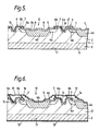
- Figures 4 to 6 illustrate a modified version of the vertical DMOSFET shown in Figures 1 to 3.
- the vertical DMOSFET shown in Figures 4 to 6 differs mainly from that shown in Figures 1 to 3 by the provision of additional or further grooves 15.
- the further grooves 15 effectively provide a boundary around each source cell 10 and extend across the grooves 8.
- the insulated gate layer 60 extends across and follows the grooves 15.
- both the grooves 8 and the further grooves 15 are formed as flat-bottomed V grooves by a selective anisotropic etching technique, although any of the etching techniques mentioned above in relation to the formation of the grooves 8 may be used. It should, of course, be appreciated that in the interests of clarity the plan view of Figure 4 does not show the bottom edges of the side walls of the further grooves 15 which would of course be visible as the further grooves 15 have a frusto-conical shape.
- the further grooves 15 are both wider and deeper than the grooves 8 with the depth of the further grooves 15 being comparable to or greater than the depth of the outer subsidiary regions 4a of the second regions 4.
- the further grooves 15 will be formed as a first step and the gate oxide provided over the further grooves 15, after any necessary cleaning, so that, as shown in Figures 5 and 6, the insulated gates 6 follow the contours of the further grooves 15.
- the further grooves 15 may have a depth (at the deepest part) of about 2 micrometres and a width of about 4 micrometres.
- the further grooves 15 may have a depth of about 4 micrometres and a width of about 6 micrometres.
- an accumulation layer forms at the surface 3′ and the surface of the grooves 15 beneath the insulated gate layer 60 which provides a relatively high mobility Conduction channel for carriers into the first region 2 so inhibiting pinch-off of the parasitic JFET and also facilitating a reduction in the on-resistance of the vertical MOSFET.
- the further grooves 15 thus act to inhibit pinch-off of the parasitic JFET (Junction FET) defined by adjacent source cells 10 which enables adjacent source cells 10 to be placed closer together so facilitating an increase in the source cell density.
- JFET parasitic JFET
- the conductivity types given above could be reversed and moreover that although the devices described above are enhancement-mode (normally off) devices, by appropriate doping of the channel areas 7 depletion-mode (normally on) devices could be formed.
- the present invention may be applied to other MOS-gated devices, for example the devices shown in Figures 1 to 6 and described above could, by replacing the substrate 9 with opposite conductivity type material, be formed as insulated gate bipolar transistors as described in, for example, GB-A-2088631 and GB-A-2072422.
- inventions 1 to 3 may be adapted to a lateral MOS-gated device, that is to a device where the main conduction path is parallel to the given surface, for example in the case of a MOSFET, where the source and drain contacts are both at the given surface.
- a field effect semiconductor device embodying the invention may be formed using other semiconductor materials, for example a III-V semiconductor material such as gallium arsenide with appropriate conventional modification of the processing technology.
Landscapes
- Junction Field-Effect Transistors (AREA)
- Insulated Gate Type Field-Effect Transistor (AREA)
Applications Claiming Priority (2)
| Application Number | Priority Date | Filing Date | Title |
|---|---|---|---|
| GB8901999A GB2227604A (en) | 1989-01-30 | 1989-01-30 | A field effect semiconductor device |
| GB8901999 | 1989-01-30 |
Publications (1)
| Publication Number | Publication Date |
|---|---|
| EP0381268A1 true EP0381268A1 (fr) | 1990-08-08 |
Family
ID=10650829
Family Applications (1)
| Application Number | Title | Priority Date | Filing Date |
|---|---|---|---|
| EP90200175A Withdrawn EP0381268A1 (fr) | 1989-01-30 | 1990-01-24 | Dispositif semi-conducteur à effet de champ |
Country Status (4)
| Country | Link |
|---|---|
| EP (1) | EP0381268A1 (fr) |
| JP (1) | JPH02238634A (fr) |
| KR (1) | KR900012376A (fr) |
| GB (1) | GB2227604A (fr) |
Cited By (2)
| Publication number | Priority date | Publication date | Assignee | Title |
|---|---|---|---|---|
| FR2692402A1 (fr) * | 1992-06-12 | 1993-12-17 | Mitsubishi Electric Corp | Dispositif à semiconducteurs comportant des couches semiconductrices de différents types de conductivité et procédé de fabrication. |
| EP1041638A1 (fr) * | 1999-04-01 | 2000-10-04 | Intersil Corporation | Dispositif à grille MOS à haute densité et son procédé de fabrication |
Citations (1)
| Publication number | Priority date | Publication date | Assignee | Title |
|---|---|---|---|---|
| US4393391A (en) * | 1980-06-16 | 1983-07-12 | Supertex, Inc. | Power MOS transistor with a plurality of longitudinal grooves to increase channel conducting area |
Family Cites Families (2)
| Publication number | Priority date | Publication date | Assignee | Title |
|---|---|---|---|---|
| JPS5242078A (en) * | 1975-09-30 | 1977-04-01 | Sanken Electric Co Ltd | Insulated gate tupe field effect transistor |
| JPS59231862A (ja) * | 1983-06-13 | 1984-12-26 | Nissan Motor Co Ltd | 縦型mosトランジスタ |
-
1989
- 1989-01-30 GB GB8901999A patent/GB2227604A/en not_active Withdrawn
-
1990
- 1990-01-24 EP EP90200175A patent/EP0381268A1/fr not_active Withdrawn
- 1990-01-29 KR KR1019900000933A patent/KR900012376A/ko not_active Withdrawn
- 1990-01-29 JP JP2016285A patent/JPH02238634A/ja active Pending
Patent Citations (1)
| Publication number | Priority date | Publication date | Assignee | Title |
|---|---|---|---|---|
| US4393391A (en) * | 1980-06-16 | 1983-07-12 | Supertex, Inc. | Power MOS transistor with a plurality of longitudinal grooves to increase channel conducting area |
Non-Patent Citations (1)
| Title |
|---|
| IEEE TRANSACTIONS ON ELECTRON DEVICES, vol. ED-31, no. 11, November 1984, pages 1570-1591, IEEE, New York, US; M.S. ADLER et al.: "The evolution of power device technology" * |
Cited By (4)
| Publication number | Priority date | Publication date | Assignee | Title |
|---|---|---|---|---|
| FR2692402A1 (fr) * | 1992-06-12 | 1993-12-17 | Mitsubishi Electric Corp | Dispositif à semiconducteurs comportant des couches semiconductrices de différents types de conductivité et procédé de fabrication. |
| US5541430A (en) * | 1992-06-12 | 1996-07-30 | Mitsubishi Denki Kabushiki Kaisha | VDMOS semiconductor device |
| EP1041638A1 (fr) * | 1999-04-01 | 2000-10-04 | Intersil Corporation | Dispositif à grille MOS à haute densité et son procédé de fabrication |
| US6188105B1 (en) | 1999-04-01 | 2001-02-13 | Intersil Corporation | High density MOS-gated power device and process for forming same |
Also Published As
| Publication number | Publication date |
|---|---|
| GB8901999D0 (en) | 1989-03-22 |
| GB2227604A (en) | 1990-08-01 |
| JPH02238634A (ja) | 1990-09-20 |
| KR900012376A (ko) | 1990-08-04 |
Similar Documents
| Publication | Publication Date | Title |
|---|---|---|
| US6916712B2 (en) | MOS-gated device having a buried gate and process for forming same | |
| EP0616372B1 (fr) | Transistor DMOS à canal court avec tranchée | |
| KR100256903B1 (ko) | 전계효과 트랜지스터 | |
| EP0633611B1 (fr) | Dispositif semi-conducteur comprenant un dispositif bipolaire à effet de champ à grille isolée | |
| US8237195B2 (en) | Power MOSFET having a strained channel in a semiconductor heterostructure on metal substrate | |
| US7645661B2 (en) | Semiconductor device | |
| US7405452B2 (en) | Semiconductor device containing dielectrically isolated PN junction for enhanced breakdown characteristics | |
| EP1286399B1 (fr) | Transistors LDMOS à effet de champ | |
| US7019360B2 (en) | High voltage power mosfet having a voltage sustaining region that includes doped columns formed by trench etching using an etchant gas that is also a doping source | |
| US5838042A (en) | DMOS device structure, and related manufacturing process | |
| EP0345380A2 (fr) | Procédé de fabrication d'un dispositif semi-conducteur | |
| US6534823B2 (en) | Semiconductor device | |
| US20070126055A1 (en) | Trench insulated gate field effect transistor | |
| US20080087952A1 (en) | Semiconductor component having a transition region | |
| US5661312A (en) | Silicon carbide MOSFET | |
| TWM516231U (zh) | 具有平面狀通道的垂直功率金氧半場效電晶體 | |
| JP2025515379A (ja) | 炭化ケイ素プレーナーmosfet素子及びその製造方法 | |
| US20220384578A1 (en) | Semiconductor device | |
| KR20170107396A (ko) | 반도체 트랜지스터 및 그 제조 방법 | |
| US5391908A (en) | Lateral insulated gate field effect semiconductor | |
| US7063975B2 (en) | Shallow trench power MOSFET and IGBT | |
| GB2227604A (en) | A field effect semiconductor device | |
| US20250241037A1 (en) | Self-aligned source contact for sic switch utilizing oxidation rate difference between poly-si and sic | |
| GB2227605A (en) | A vertical field effect semiconductor device | |
| US20240030307A1 (en) | A method of manufacturing a vertical oriented semiconductor device as well as a corresponding vertical oriented semiconductor device obtained by such a method |
Legal Events
| Date | Code | Title | Description |
|---|---|---|---|
| PUAI | Public reference made under article 153(3) epc to a published international application that has entered the european phase |
Free format text: ORIGINAL CODE: 0009012 |
|
| AK | Designated contracting states |
Kind code of ref document: A1 Designated state(s): DE FR GB IT NL |
|
| STAA | Information on the status of an ep patent application or granted ep patent |
Free format text: STATUS: THE APPLICATION IS DEEMED TO BE WITHDRAWN |
|
| 18D | Application deemed to be withdrawn |
Effective date: 19910209 |