EP0381332A2 - Simulation de circuits ayant des parties analogiques et des parties numériques - Google Patents
Simulation de circuits ayant des parties analogiques et des parties numériques Download PDFInfo
- Publication number
- EP0381332A2 EP0381332A2 EP90300469A EP90300469A EP0381332A2 EP 0381332 A2 EP0381332 A2 EP 0381332A2 EP 90300469 A EP90300469 A EP 90300469A EP 90300469 A EP90300469 A EP 90300469A EP 0381332 A2 EP0381332 A2 EP 0381332A2
- Authority
- EP
- European Patent Office
- Prior art keywords
- circuit
- analogue
- digital
- value
- input signal
- Prior art date
- Legal status (The legal status is an assumption and is not a legal conclusion. Google has not performed a legal analysis and makes no representation as to the accuracy of the status listed.)
- Granted
Links
Images
Classifications
-
- G—PHYSICS
- G06—COMPUTING OR CALCULATING; COUNTING
- G06J—HYBRID COMPUTING ARRANGEMENTS
- G06J1/00—Hybrid computing arrangements
-
- G—PHYSICS
- G06—COMPUTING OR CALCULATING; COUNTING
- G06F—ELECTRIC DIGITAL DATA PROCESSING
- G06F30/00—Computer-aided design [CAD]
- G06F30/30—Circuit design
- G06F30/36—Circuit design at the analogue level
- G06F30/367—Design verification, e.g. using simulation, simulation program with integrated circuit emphasis [SPICE], direct methods or relaxation methods
Definitions
- the present invention relates to the simulation of the operation of a circuit having both analogue circuit parts and digital circuit parts connected together.
- circuit level simulators Simulators which simulate systems through analysis of the currents and voltages in the lowest level components are termed "circuit level” simulators. Although such simulators are usually quite accurate and can simulate both analogue and digital circuit blocks, they operate very slowly so that a long period of time is required to obtain a full simulation of the behaviour of the overall system.
- Another kind of simulator operates by utilising the behavioural description of the functional building blocks, such as for example logic gates, operational amplifiers, filters, etc.
- a simulator When such a simulator is used to simulate the operation of digital circuits it is known as a "logic simulator" and uses digital logic values as the signals to provide the interaction between the blocks.
- Logic simulators cannot simulate the operation of analogue circuits because of the continuously variable nature of the signals to be fed from one circuit block to another.
- logic simulators can simulate the operation of digital circuits quite quickly and can readily be programmed to provide a reasonable simulation of a digital system in a relatively short period of time.
- event-driven logic simulator There are two common types of logic simulators; event-driven and levelised compiled code simulators.
- event-driven logic simulator the response of a circuit is only evaluated when its inputs are changed, and the simulator must employ an event queue in order to maintain the changes at different parts of the circuit in step. The servicing of the event queue requires a lot of processing to be done by the computer, and consequently slows down the operation of the simulator.
- levelised compiled code logic simulator the inputs to a circuit are set up and maintained at those values while each logic element is evaluated in the order of signal flow through the circuit. The sequential nature of the analysis makes evaluation much simpler and therefore faster than in the case of an event-driven simulator.
- Enhancements of event-driven logic simulators have been proposed to enable them to cope with analogue circuit blocks and these have relied upon the use of real numbers indicating the actual values of voltage signals at sampling instants in the operation of both analogue and digital circuits.
- Such enhancements of logic simulators tend to slow down their operation so that a longer period of time is required to simulate the operation of digital circuits than is possible when only digital logic values are transmitted between the blocks.
- a method of simulating by means of a digital computer the operation of a circuit including analogue circuit blocks the circuit composed of analogue circuit blocks being represented by a computer program in which each analogue circuit block is represented by a procedure call including details of input signal name(s) and value(s), output signal name(s) and value(s), the operational parameters of the block and the sampling instant for the evaluation of each output signal value, each connection between the blocks is represented by the use of the same signal name for an output signal and an input signal, and real numbers are used to indicate the actual values of the input and output signals, each sampling instant for the evaluation of an output signal value being the time at which that value has changed by a predetermined amount since the previous sampling instant, wherein the values of the output signals from the procedure calls representing analogue circuit blocks are evaluated at sampling times common to all the procedure calls, each common sampling time being selected as the earliest of the sampling instants provided by the procedure calls of all the analogue circuit blocks included in the circuit.
- the invention also includes apparatus for carrying out the method.
- the simulation of the operation of a circuit composed of analogue circuit blocks may be combined with a logic simulator of event-driven or levelised compiled code type modelling the operation of a circuit composed of digital circuit blocks so as to provide a model of a circuit including an analogue sub-system and a digital sub-system.
- the logic simulator may be a commercially available one, in which case the analogue sub-system model will include an analogue/digital interface to produce digital input signals for the logic simulator and to receive digital output signals from the logic simulator to represent the interconnections between the two sub-systems.
- the sub-system model may include at least one one-bit digital-to-analogue converter responsive to a digital logic value received as an input from the digital sub-system model and/or at least one one-bit analogue-to-digital converter responsive to an analogue signal value to produce an output digital logic value transmitted to the digital sub-system model.
- the analogue sub-system model may be a levelised compiled code model. Because the signals occurring in analogue are continuous functions of time and the digital computer requires numbers to process, it is necessary to sample the analogue signals at discrete time points and process the values obtained. In a procedure call modelling an analogue electrical circuit block the sampling instants are to be set when by the change in an output signal of the block since the previous sampling instant is a predetermined voltage or current step. An example of a voltage step would be 1% of the maximum possible variation in the output signal voltage. Such a procedure for setting the sampling instant when applied to all the analogue circuit blocks in the sub-system could give rise to several different sampling instants.
- the model of the analogue sub-system is of the levelised compiled code type it is necessary to use the same sampling instants in all the analogue circuit blocks in the sub-system and this is achieved by each time selecting the earliest sampling instant among all the analogue circuit blocks in the sub-system and using that instant in all the analogue circuit blocks. In that way the accuracy of the analogue simulation is at least as good as that set by the user when he defined the voltage steps.
- the value of the output voltage of the block(s) at the sampling instant must be represented by a number which can be transmitted to the next block(s) in the circuit.
- the time scale in the analogue circuit sub-system model will not, in general, correspond to real time but it must match the time scale used in the logic simulator for the digital circuit blocks.
- the analogue circuit sub-system may include a feedback path so that an input to part of the circuit is derived from an output of that part.
- the levelised compiled code simulation of the analogue sub-system may be arranged to model the operation of the feedback path.
- the response of the circuit may be determined by a process of progressive adjustments of the fed back input resulting from taking into account the previous adjustment of that input, whilst any external inputs to the circuit are held constant. The adjustment is repeated a number of times until a stable fed back input and a stable output are obtained. While the adjustments are being calculated the signal values in parts outside the feedback loop, both analogue and digital, do not change. Two or more unconnected feedback circuits can be processed at the same time.
- each cell contains the name or source of the, or each, input signal to the particular block; the name or destination of the, or each, output signal from the particular block, and some representation of the signal processing properties of the particular block from which the value of the output signal(s) generated by the block in response to the input signal(s) can be derived.
- the externally originating signals which form the inputs, analogue and/or digital, to the circuit are set to the required initial values, and are then changed in the same way as they would in the operation of the circuit itself.
- the input signals to the digital part of the circuit have digital logic values, such as "high” and “low” or "0" and "1".
- An input signal to the analogue part of the circuit are samples taken from a continuous signal which is a continuous function of time at given sampling instants.
- the changes in the two types of input signal, analogue and digital must be kept in synchronism and may take place at a slower rate than real time to allow time for the model of the circuit to respond to the changes.
- the processing speed of the computer is high enough or the digit rate of the digital input signals and the frequency content of the analogue input signals are low enough, the model may operate on samples in real time.
- the procedure calls representing blocks receiving the input signals from outside the circuit are processed by the computer to determine what output signals they will produce, and the resulting signals are applied as inputs to other procedure calls.
- the signals received by these other procedure calls are processed, resulting in other signals being generated and applied to further procedure calls, and so on.
- the processing of the procedure calls follows the various signal paths through the circuit with the final result that one or more output signals are generated.
- the computer is arranged to display the output signals to the user as the response of the model of the circuit to the input signals.
- the computer may also display the values of the intermediate signals to aid the understanding of the operation of the circuit model. Facilities may be provided for changing the parameters of some procedure calls representing circuit blocks so that the user can see the effect of changing component values or performance characteristics on the operation of the circuit.
- the simulation program of the computer is divided into two distinct parts, a first part providing a model of the digital blocks in the circuit and a second part providing a model of the analogue blocks in the circuit.
- the first part of the program that providing the model of the digital blocks in the circuit, is a conventional logic simulator program.
- the second part of the program, that providing the model of the analogue blocks in the circuit not only handles the transmission of the signals between the analogue blocks but it also provides the conversion of the analogue signal values to digital logic values for signals which are applied to a digital block from an analogue block, and the conversion of digital logic values to analogue signal values for signals which are received by an analogue block from a digital block.
- the analogue to digital conversion will involve the production of a "1” if the analogue voltage is above a threshold value and the production of a "0" if it is below that value.
- the digital to analogue conversion may result in a first voltage (say, 5 volts) being produced in response to a "1” and a second voltage (say, 0 volts) being produced in response to a "0".
- the input and output signals of the analogue circuit blocks are usually measured in terms of voltage, there are forms of analogue circuit system component where some other electrical or mechanical variable forms the input and/or output signal, such other forms of component can also be modelled by the procedure calls.
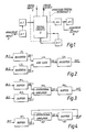
- FIG. 1 shows a hypothetical circuit having digital circuits D and analogue circuit blocks A1, A2, A3, A4 and A5.
- the blocks A2 and A3 are connected to apply input signals to the digital circuits D
- the blocks A3 and A4 are connected to receive input signals from the digital circuits D.
- the analogue/digital interface is represented by the broken line I; this interface represents the conversion of analogue signals to digital logic signals for signals which are being applied to the digital circuits D from the analogue blocks A1 - A5, and the conversion of digital logic signals to analogue signals for signals received by the analogue blocks A1 - A5 from the digital circuits D.
- Digital logic input signals from an external source are applied to the digital circuits D along an input E.
- Digital logic output signals from the digital circuits D are applied to an external circuit along an output F.
- Analogue signals in the form of sampled values are applied as inputs to the analogue block A1 along an input G.
- Analogue output signals from the analogue block A4 appear on an output H, again in the form of sampled values.
- the logic simulator When simulating the operation of the circuit shown in Figure 1, the first part of the program, the logic simulator, provides a model of the digital circuits D and the second part of the program provides a model of the analogue circuit blocks A1, ..., A5 as well as the analogue/digital interface I.
- program is not limited to simulating the operation of the circuit shown in Figure 1, but can simulate the operation of any circuit.
- An advantage of separating the analogue circuit blocks from the digital ones in the simulation by providing separate simulation programs for the analogue part and the digital part of the circuit is that is necessary to transmit analogue signal values only in the analogue part, because the digital part need transmit only digital logic values.
- Figure 2 shows an example of a digital circuit having two inverters L1 and L2 to which input signals IN1 and IN2 are respectively applied.
- the outputs of the inverters L1 and L2 which are SIG1 and SIG2 respectively are applied to the inputs of an AND-gate L3.
- a further inverter L4 receives the output SIG3 and the AND-gate L3 to produce the output signal.
- the logic simulator includes a library of logic elements including an inverter and an AND-gate and the information in the library includes the fact that an inverter has one input signal and one output signal, and the fact that an AND-gate has two input signals and one output signal.
- the order of the procedure calls in the program is critical because the statements are executed sequentially and it is necessary for the values of SIG1 and SIG2 to be worked out before the output SIG3 of the AND-gate is derived from the values of SIG1 and SIG2.
- the signals IN1, IN2, SIG1, SIG2, SIG3 and OUT can assume only logic values such as 0 and 1 or high and low.
- Figure 3 shows an example of an analogue circuit having buffers M1 and M2 to which input signals IN1 and IN2 are respectively applied.
- the outputs of the buffers M1, M2, which are named SIG1 and SIG2 are applied to the non-inverting and inverting inputs respectively of an operational amplifier M3.
- the output signal of the operational amplifier M3 is named SIG3 and is applied through a buffer M4 to produce the output signal OUT.
- the library records the parameters that determine the performance of the circuit elements.
- the program it is necessary for the program to provide a mechanism for handling circuit evaluation times.
- the signals in the model are evaluated whenever one of the inputs of the circuit changes, this being possible because the change from one state to another of the input and output signals is assumed to be instantaneous.
- the program For an analogue circuit model the program must determine the times of evaluation of the input and output signals because the values of these signals can be varying all the time and it is possible for an output value of a circuit to be varying even though the inputs to that circuit are constant.
- the program determines the evaluation times by reference to a voltage step.
- This voltage step is an increment or decrement in the voltage concerned and may be an absolute value, such as, for example, 1 millivolt.
- the program provides an opportunity for the user to define a voltage step appropriate to each analogue circuit element.
- the program calculates the future time, relative to the present time at which the specified voltage step will be reached in the output value of the circuit on the basis of the parameters specified for that circuit in the library.
- the future times for all of the circuit elements in the circuit are then compared and the earliest of these is selected by the program for use by all the circuit elements in the circuit.
- the interval between the present and future times is termed the "retrigger time" and can vary throughout the period of operation of the circuit.
- the value of the retrigger time is initially set at an arbitrarily high level, but after the program has worked through all of the circuit elements the retrigger time will have the value required by the element having the tightest timing requirement.
- the resulting program structure for the circuit shown in Figure 3 is as follows:- Procedure (arguments) Buffer (M1, IN1, SIG1, ... parameters ..., Max_voltage_step, retrigger_time); Buffer (M2, IN2, SIG2, ... parameters ..., Max_voltage_step, retrigger_time); OPAMP (M3, SIG1, SIG2, SIG3, ... parameters ..., Max_voltage_step, retrigger_time); Buffer (M4, SIG3, OUT, ... parameters ..., Max_voltage_step, retrigger_time).
- Each cell includes the reference number - M1, M2, etc., of the circuit element which is used as a pointer to memory locations where previous state values may be recorded for use in the modelling algorithms.
- the circuit parameters are not required for digital devices because the logical operation performed by any such device is determined by its name. In the case of analogue circuit elements there could, for example, be operational amplifiers having different gains and different slew rates.
- a third difference is in the provision of the maximum voltage step and the retriggering time which are used as described above.
- the model is also evaluated when an input to the analogue circuit as a whole is changed, for example, in response to a change in a digital logic signal applied to the analogue sub-system. This means that each model of a circuit element must have the ability to evaluate its output at any time and not simply at the specified voltage steps.
- the program inserts one-bit analogue-to-digital converters or digital-to-analogue converters for carrying out the conversion between digital logic values and analogue signal values.
- Analogue circuits and hence the models representing them, sometimes contain feedback where the output of a block in a circuit is fed back to its own input or that of an earlier block in the circuit. In this situation it is impossible to work through the circuit from input to output to determine the signal levels at each block, but if the feedback loop is broken, it can be done, although there will remain a feedback signal which must be taken into account.
- Figure 4 shows an example of a circuit with feedback.
- An input signal IN2 is applied as an input to a buffer N1, the output, SIG2, of which is applied to the non-inverting input of an operational amplifier N2.
- the output signal, SIG3, of the amplifier N2 is applied as the input to a buffer N3 the output of which forms the output signal OUT of the circuit.
- the signal OUT is also fed back to be applied to the inverting input of the amplifier N2.
- the model program compiled by the simulators follows the principles outlined above with reference to Figure 3 except that it contains a loop for calculating the feedback signal.
- the program to model that circuit is as follows;-
- the second program provides a method of feedback management which may be summarised as follows. First some terminology will be clarified. The model is invoked at various instants, and following each instant a number of iterations round the feedback loop(s) are made to establish the correct value of the feedback signal(s). It is in this context that the terms "iteration” and “invocation” are used in the following description.
- the program includes a procedure which is applied to a signal that is fed back. At each invocation this procedure estimates the value that the feedback signal should have at that instant.
- Several iterations are made of a program loop for evaluating the feedback signal. The iterations are terminated when the difference between the value of the feedback signal and an estimated value derived from previous values of the feedback signal becomes sufficiently small, for example, a predetermined fraction of the voltage step allocated to the circuit block.
- Some circuit blocks require a memory of past state information, and these actually have two copies of that information.
- One is known as the master copy, and the other as the working copy.
- the master copy of the past state information is copied into the working copy of the past state information, and it is the working copy that is used to calculate the model output. This procedure is followed so that each iteration within an invocation is calculated on the basis of correct past information - if this were not done then each iteration would update the past state information, which is required to be the past state at the previous retrigger time and therefore must be fixed until the next retrigger time.
- the working copy of the information is what should be the master copy for the next retrigger time and so, after each invocation of the model, the pointers indicating the working and master copies are swapped over.
- the initial value used for the feedback signal is actually the value of that signal generated on the previous invocation. As that value was generated at an earlier time instant it is not correct for the present time instant.
- the output signals of the circuit blocks are evaluated and then the procedure for estimating the value of the feedback signal is called and the difference between the estimated value and the obtained value is measured. This difference is recorded as a criterion as to whether or not the feedback signal estimate is good enough; if the difference between estimated value and the obtained value on a subsequent iteration is smaller than a given fraction of the first difference (e.g. by a factor of 20), then the estimate is deemed good enough.
- the first difference is dependent on the voltage step size of the immediately preceding block, and what is required is to make sure that the error in estimating the feedback value is small relative to that voltage step size.
- the procedure for estimating the value of the feedback signal will modify that value in preparation for the second iteration.
- the latest estimated value is a small fraction of the way from the last estimated value towards the last obtained value. In a stable system, moving the estimated value towards the obtained value will always cause the next obtained value to move in the direction towards the estimated value. A small change only is made on the second iteration, in order that the sensitivity to changes in the estimated value of the obtained value can be measured on the next iteration.
- the procedure for estimating the value of the feedback signal can evaluate that sensitivity, and can forecast the next estimated value based on that sensitivity in such a way that in a purely linear system the two values will coincide.
- a further algorithm is applied. This measures the present difference between the estimated value and the obtained value, and moves the estimated value by a small fraction of that difference (e.g. 1/8). If this fails the amount of movement is doubled on successive iterations. In the event of overshoot a small fraction of the last increment of the estimate is applied in the opposite direction. Essentially the algorithm applied is one of moving the estimate towards the obtained values in increasing jumps, until an overshoot occurs, in which case the search is taken back in the other direction with the jump size scaled down by a small fraction (for example, 1/8). The result (or consequence) is that searching for the correct estimated value is done to increasingly finer resolution. This is therefore inherently stable, and is flexible enough to permit several feedback signals to be modified at the same time.
- the parameters of the cell may include the transfer function in the form of a Laplace transform or a Z-transform, and the program may be arranged to calculate the output signal value from the current input signal value and stored previous signal values taking into account the time scale.
Landscapes
- Engineering & Computer Science (AREA)
- Computer Hardware Design (AREA)
- Theoretical Computer Science (AREA)
- Physics & Mathematics (AREA)
- Evolutionary Computation (AREA)
- General Physics & Mathematics (AREA)
- General Engineering & Computer Science (AREA)
- Geometry (AREA)
- Microelectronics & Electronic Packaging (AREA)
- Mathematical Physics (AREA)
- Automation & Control Theory (AREA)
- Fuzzy Systems (AREA)
- Software Systems (AREA)
- Tests Of Electronic Circuits (AREA)
- Test And Diagnosis Of Digital Computers (AREA)
Applications Claiming Priority (2)
| Application Number | Priority Date | Filing Date | Title |
|---|---|---|---|
| GB8902464 | 1989-02-03 | ||
| GB898902464A GB8902464D0 (en) | 1989-02-03 | 1989-02-03 | Improvements in or relating to the simulation of circuits having analogue parts and digital parts |
Publications (3)
| Publication Number | Publication Date |
|---|---|
| EP0381332A2 true EP0381332A2 (fr) | 1990-08-08 |
| EP0381332A3 EP0381332A3 (fr) | 1991-09-25 |
| EP0381332B1 EP0381332B1 (fr) | 1997-11-05 |
Family
ID=10651098
Family Applications (1)
| Application Number | Title | Priority Date | Filing Date |
|---|---|---|---|
| EP90300469A Expired - Lifetime EP0381332B1 (fr) | 1989-02-03 | 1990-01-17 | Simulation de circuits ayant des parties analogiques et des parties numériques |
Country Status (4)
| Country | Link |
|---|---|
| EP (1) | EP0381332B1 (fr) |
| JP (1) | JPH02242375A (fr) |
| DE (1) | DE69031661T2 (fr) |
| GB (1) | GB8902464D0 (fr) |
Cited By (2)
| Publication number | Priority date | Publication date | Assignee | Title |
|---|---|---|---|---|
| EP0481117A1 (fr) * | 1990-10-18 | 1992-04-22 | Siemens Aktiengesellschaft | Méthode pour accélérer la simulation lors de la conception assistée par ordinateur de circuits électroniques et systèmes |
| EP0762303A3 (fr) * | 1995-08-30 | 2000-08-02 | Sun Microsystems, Inc. | Simulateur à réflux |
Families Citing this family (1)
| Publication number | Priority date | Publication date | Assignee | Title |
|---|---|---|---|---|
| CN101339409B (zh) * | 2008-08-14 | 2010-04-14 | 上海交通大学 | 基于等效模型变换的数模与模数转换卡辨识方法 |
Family Cites Families (1)
| Publication number | Priority date | Publication date | Assignee | Title |
|---|---|---|---|---|
| CA1300265C (fr) * | 1987-06-22 | 1992-05-05 | William Curtis Newman | Simulateur de diagrammes synoptiques |
-
1989
- 1989-02-03 GB GB898902464A patent/GB8902464D0/en active Pending
-
1990
- 1990-01-17 EP EP90300469A patent/EP0381332B1/fr not_active Expired - Lifetime
- 1990-01-17 DE DE69031661T patent/DE69031661T2/de not_active Expired - Fee Related
- 1990-02-02 JP JP2024282A patent/JPH02242375A/ja active Pending
Cited By (2)
| Publication number | Priority date | Publication date | Assignee | Title |
|---|---|---|---|---|
| EP0481117A1 (fr) * | 1990-10-18 | 1992-04-22 | Siemens Aktiengesellschaft | Méthode pour accélérer la simulation lors de la conception assistée par ordinateur de circuits électroniques et systèmes |
| EP0762303A3 (fr) * | 1995-08-30 | 2000-08-02 | Sun Microsystems, Inc. | Simulateur à réflux |
Also Published As
| Publication number | Publication date |
|---|---|
| DE69031661T2 (de) | 1998-03-12 |
| JPH02242375A (ja) | 1990-09-26 |
| DE69031661D1 (de) | 1997-12-11 |
| EP0381332A3 (fr) | 1991-09-25 |
| GB8902464D0 (en) | 1989-03-22 |
| EP0381332B1 (fr) | 1997-11-05 |
Similar Documents
| Publication | Publication Date | Title |
|---|---|---|
| US5105373A (en) | Method of simulating the operation of a circuit having analog and digital circuit parts | |
| US5406497A (en) | Methods of operating cell libraries and of realizing large scale integrated circuits using a programmed compiler including a cell library | |
| Kalman | Design of a self-optimizing control system | |
| US6321363B1 (en) | Incremental simulation using previous simulation results and knowledge of changes to simulation model to achieve fast simulation time | |
| US7203632B2 (en) | HDL co-simulation in a high-level modeling system | |
| US5359535A (en) | Method for optimization of digital circuit delays | |
| Woodward et al. | An application of Bayesian methods in SPC | |
| US5650946A (en) | Logic simulator which can maintain, store and use historical event records | |
| CN115083546B (zh) | 一种基于从头算分子动力学方法计算材料离位阈能的方法 | |
| US20130125074A1 (en) | System and method for designing digital circuitry with an activity sensor | |
| KR100267362B1 (ko) | 예견제어장치 | |
| EP0381332A2 (fr) | Simulation de circuits ayant des parties analogiques et des parties numériques | |
| JP2005071370A (ja) | 回路設計のアクティビティファクタを決定するためのシステムおよび方法 | |
| Koksal et al. | A program for the design of linear time invariant control systems: CDMCAD | |
| EP0507535B1 (fr) | Un système pour déterminer le fonctionnement d'un circuit intégré | |
| US5461575A (en) | Simulation of sequential circuits for calculating timing characteristics to design/manufacture a logic network | |
| Parkinson | Simulated variance optimization for robust design | |
| JPH03269736A (ja) | 計算機システム | |
| CN121389946B (zh) | 刚性电路的步长确定方法、仿真方法、电子设备及产品 | |
| Kushner et al. | A versatile method for the Monte Carlo optimization of stochastic systems | |
| JPH07334070A (ja) | プロセスシミュレータ | |
| Lindemann | Employing the randomization technique for solving stochastic Petri net models | |
| Juan-Chico et al. | AUTODDM: AUTOmatic characterization tool for the Delay Degradation Model | |
| JPH1049555A (ja) | 回路設計におけるタイミング解析方法 | |
| Fu | Modeling and analysis of discrete tandem production lines using continuous flow models |
Legal Events
| Date | Code | Title | Description |
|---|---|---|---|
| PUAI | Public reference made under article 153(3) epc to a published international application that has entered the european phase |
Free format text: ORIGINAL CODE: 0009012 |
|
| AK | Designated contracting states |
Kind code of ref document: A2 Designated state(s): DE FR GB IT NL |
|
| PUAL | Search report despatched |
Free format text: ORIGINAL CODE: 0009013 |
|
| AK | Designated contracting states |
Kind code of ref document: A3 Designated state(s): DE FR GB IT NL |
|
| 17P | Request for examination filed |
Effective date: 19920324 |
|
| 17Q | First examination report despatched |
Effective date: 19950202 |
|
| GRAG | Despatch of communication of intention to grant |
Free format text: ORIGINAL CODE: EPIDOS AGRA |
|
| GRAH | Despatch of communication of intention to grant a patent |
Free format text: ORIGINAL CODE: EPIDOS IGRA |
|
| GRAH | Despatch of communication of intention to grant a patent |
Free format text: ORIGINAL CODE: EPIDOS IGRA |
|
| GRAA | (expected) grant |
Free format text: ORIGINAL CODE: 0009210 |
|
| ITF | It: translation for a ep patent filed | ||
| AK | Designated contracting states |
Kind code of ref document: B1 Designated state(s): DE FR GB IT NL |
|
| REF | Corresponds to: |
Ref document number: 69031661 Country of ref document: DE Date of ref document: 19971211 |
|
| ET | Fr: translation filed | ||
| PLBE | No opposition filed within time limit |
Free format text: ORIGINAL CODE: 0009261 |
|
| STAA | Information on the status of an ep patent application or granted ep patent |
Free format text: STATUS: NO OPPOSITION FILED WITHIN TIME LIMIT |
|
| 26N | No opposition filed | ||
| REG | Reference to a national code |
Ref country code: GB Ref legal event code: IF02 |
|
| PGFP | Annual fee paid to national office [announced via postgrant information from national office to epo] |
Ref country code: GB Payment date: 20061213 Year of fee payment: 18 |
|
| PGFP | Annual fee paid to national office [announced via postgrant information from national office to epo] |
Ref country code: DE Payment date: 20070131 Year of fee payment: 18 |
|
| PGFP | Annual fee paid to national office [announced via postgrant information from national office to epo] |
Ref country code: IT Payment date: 20070627 Year of fee payment: 18 |
|
| PGFP | Annual fee paid to national office [announced via postgrant information from national office to epo] |
Ref country code: FR Payment date: 20070103 Year of fee payment: 18 |
|
| PGFP | Annual fee paid to national office [announced via postgrant information from national office to epo] |
Ref country code: NL Payment date: 20071219 Year of fee payment: 19 |
|
| GBPC | Gb: european patent ceased through non-payment of renewal fee |
Effective date: 20080117 |
|
| PG25 | Lapsed in a contracting state [announced via postgrant information from national office to epo] |
Ref country code: DE Free format text: LAPSE BECAUSE OF NON-PAYMENT OF DUE FEES Effective date: 20080801 |
|
| REG | Reference to a national code |
Ref country code: FR Ref legal event code: ST Effective date: 20081029 |
|
| PG25 | Lapsed in a contracting state [announced via postgrant information from national office to epo] |
Ref country code: GB Free format text: LAPSE BECAUSE OF NON-PAYMENT OF DUE FEES Effective date: 20080117 |
|
| PG25 | Lapsed in a contracting state [announced via postgrant information from national office to epo] |
Ref country code: FR Free format text: LAPSE BECAUSE OF NON-PAYMENT OF DUE FEES Effective date: 20080131 |
|
| PG25 | Lapsed in a contracting state [announced via postgrant information from national office to epo] |
Ref country code: IT Free format text: LAPSE BECAUSE OF NON-PAYMENT OF DUE FEES Effective date: 20080117 |
|
| NLV4 | Nl: lapsed or anulled due to non-payment of the annual fee |
Effective date: 20090801 |
|
| PG25 | Lapsed in a contracting state [announced via postgrant information from national office to epo] |
Ref country code: NL Free format text: LAPSE BECAUSE OF NON-PAYMENT OF DUE FEES Effective date: 20090801 |