EP0481117A1 - Méthode pour accélérer la simulation lors de la conception assistée par ordinateur de circuits électroniques et systèmes - Google Patents
Méthode pour accélérer la simulation lors de la conception assistée par ordinateur de circuits électroniques et systèmes Download PDFInfo
- Publication number
- EP0481117A1 EP0481117A1 EP90120006A EP90120006A EP0481117A1 EP 0481117 A1 EP0481117 A1 EP 0481117A1 EP 90120006 A EP90120006 A EP 90120006A EP 90120006 A EP90120006 A EP 90120006A EP 0481117 A1 EP0481117 A1 EP 0481117A1
- Authority
- EP
- European Patent Office
- Prior art keywords
- simulation
- circuit
- analog
- event
- simulated
- Prior art date
- Legal status (The legal status is an assumption and is not a legal conclusion. Google has not performed a legal analysis and makes no representation as to the accuracy of the status listed.)
- Withdrawn
Links
Images


Classifications
-
- G—PHYSICS
- G06—COMPUTING OR CALCULATING; COUNTING
- G06F—ELECTRIC DIGITAL DATA PROCESSING
- G06F30/00—Computer-aided design [CAD]
- G06F30/30—Circuit design
- G06F30/36—Circuit design at the analogue level
- G06F30/367—Design verification, e.g. using simulation, simulation program with integrated circuit emphasis [SPICE], direct methods or relaxation methods
Definitions
- register transfer simulation is carried out at the block level or register transfer level.
- the circuit is broken down into block functions and the interaction of the blocks is simulated.
- the description is also made using HLL constructs or using functional blocks e.g. RAM, ALU, ROM.
- functional blocks e.g. RAM, ALU, ROM.
- the functional description of the input / output behavior is created with discrete and specified time conditions.
- circuits at gate or logic level takes place by means of functional blocks, e.g. RAM, ROM, or gates, e.g. NAND, AND, OR, NOT.
- the logical description of these blocks or gates contains Boolean equations and delay times. Discrete values (Boolean variables and discrete states 0, 1, U, X %) are used.
- the simulation of the timing behavior of logic circuits is made possible by assigning delay times to gates.
- the so-called switch level is particularly suitable for the treatment of MOS circuits.
- a circuit model at this level is described using transistors as switches.
- the transistors are described using simple algebraic equations and difference equations. For the transistors, only the states conductive, blocked and open input are taken into account. This corresponds to the discrete signal values 0, 1 and X at the nodes.
- different signal strengths and specific MOS properties can also be treated in the form of further discrete states.
- the timing simulation is only used for MOS circuits with low feedback circuit stages. Gates (function and delay) or rough models for transistors are used to describe a circuit model at this level. The description is made using network equations, Boolean equations and a time grid with discrete values. Network equations are only solved approximately.
- the circuit is described by electrical components (resistors, capacitors, transistors ...) and their combination.
- the behavior is described using time-dependent, continuous physical variables, e.g. l (t), U (t), Q (t).
- Different equivalent circuits can be selected as the transistor model, which means that different levels of accuracy can be achieved in the simulation. The differences lie in the idealization of the characteristic equations, the neglect of the coupling capacities and the simplification of the returns.
- the mathematical description of the electrical components consists of a set of differential equations that take Kirchhoff's laws into account. In the simulation, a network analysis with continuous values for signals is carried out.
- process simulation is used to examine technological conditions in the manufacture of integrated circuits.
- This simulation level forms the lower end of the hierarchy of simulation levels. Diffusion, implantation, etching, lacquer profiles and multidimensional effects are described with the equations of semiconductor physics.
- numerical models and methods are used.
- the described simulation levels each belong to one of two categories, which are referred to as digital or analog simulation.
- the digital simulation extends over the system, register transfer and logic level. Switch and timing levels can be assigned to both digital simulation and analog simulation (see Table 1).
- the user can design his logic, i.e. verify the conformity of the circuit function with predetermined Boolean functions.
- signal profiles are processed using discrete states e.g. 0 and 1 and idealized edges are taken into account. Edge uncertainties are marked in state X (undefined).
- Compliance with fan-in / fan-out conditions can be simulated using load factors.
- time conditions can be taken into account in the timing level, whereby, in contrast to static simulation, the functionality of the overall circuit can be verified with given delay times of subcircuits.
- the developer can carry out different analyzes, e.g. Perform worst case path analysis or minimax path analysis.
- the analog simulation which is also called electrical simulation, extends over the circuit, device and process level.
- the circuit developer understands analog simulation primarily to mean simulation at the circuit level and possibly at the switch and timing level (see Table 1).
- digital simulation the user can use analog simulation to perform both the function of the circuit design, i.e. verify the correspondence of the logic circuit function with the aid of predetermined Boolean functions as well as the timing of the circuit design.
- the signals are assigned continuous or very finely graduated discrete numerical values in the analog simulation, which is why edge steepness and level values can be read from the analog signals shown in this way. Time delays and phase shifts can also be read directly from the analog time functions.
- the digital and the analog simulation types can be connected to one another in different ways. Therefore, depending on the degree of coverage of the different simulation levels during a simulation run, a distinction is made between the simulation types single-level simulation (simple simulation), multi-level simulation (multi-level simulation) and mixed-mode simulation.
- the circuit to be simulated which can also be structured hierarchically, is mapped to a simulation model in a simulation level.
- the entire circuit is described throughout on a single circuit description level.
- the simulator only works on this one simulation level for the one-level simulation. Because of the restriction to a circuit description level and a simulation level, only one library is required for the one-level simulation.
- the circuit to be simulated, also hierarchically structured is optionally mapped to different simulation models, which can comprise one or more levels.
- the simulator works with exactly one description language, with which the circuit can be described on one or more related levels.
- the simulation run moves in one or more levels related to the description language. For example, using a description language, a circuit can be described and simulated both at the register transfer level and at the logic level.
- mixed-mode simulation a circuit to be simulated, also hierarchically structured, is finally mapped onto simulation models at different levels. Different circuit parts can be assigned to different simulation levels. These circuit parts can be hierarchical or e.g. follow a critical path.
- the simulator works on all levels simultaneously. Mixed mode simulation is always a combination of logic and circuit simulation. Within a simulation run, individual circuit parts are modeled with different accuracy and described on different circuit description levels. For this reason, several libraries are used side by side for the different circuit description and simulation levels.
- the sequence control and the calculation of the element functions are also important for the characterization of a simulator.
- those times are particularly important at which a change in the signal state occurs or is to be expected. All of these times form either a heterogeneous or a homogeneous time grid. In the case of a heterogeneous time grid, the time intervals between two successive grid points are different, but they are the same for the homogeneous time grid.
- the complete model is calculated for every possible point in time.
- An element of the simulation model is always calculated regardless of the signal curve if all inputs are supplied with valid values.
- the complete data record must be built up and buffered for each point in time.
- event control In contrast to the rather complex methods of time control and data flow control, so-called event control only calculates the element functions of those elements that are relevant for the time in question, i.e. at the inputs there is a change in the input signals.
- the invention is based on the object of specifying a method for mixed mode simulation of electrical circuits which is as efficient as possible on the basis of event control. This object is achieved by a method for simulating electronic circuits and systems with features according to claim 1.
- the design of circuits and their verification is carried out with the help of simulations on the model levels summarized in Table 2.
- the system level represents the highest level of abstraction fe and the circuit level represent the deepest level of abstraction of the hierarchy.
- the aim of the simulation on the model levels mentioned is to know the behavior of a circuit to be examined depending on input variables (stimuli, circuit parameters) and (below the system level) on time.
- An important distinguishing feature between the model levels is the type of time handling:
- the register transfer level and in particular the logic level is generally based on a fixed, discrete time grid, over which the possible changes in state are considered, while the timing level and the circuit level reproduce possible status changes as functions over the continuous time axis. To describe the preferred exemplary embodiment, the circuit level and the logic level are therefore described as representative of the types of time treatment mentioned.
- D1 and D2 must first be loaded (S1) and then starting from X2 with S4, S5, S6, S2 to generate the start assignment of the EVENTLIST event list system.
- An event cycle always has its starting point at X1.
- the event cycles (S2, S3, S4, S5, S6) are then generated dynamically (that is, depending on the activity profile of the circuit system to be simulated) and processed according to a partial order of the events represented by the event list system EVENTLIST.
- t n + 1 already be determined as the current point in time of the approximate solution. Furthermore, the approximate solutions x0, ... xn at the times t0, ... tn are assumed to be known.
- the interpolation polynomials P (t; k, n + 1) and P (t; k + 1, n + 1) must also be defined in an analogous manner.
- the Newton method is then used to solve the system (5) in the second step with the starting solution applied.
- the interpolation polynomial P (t; k, n) thus serves as a predictor formula for x n + 1 .
- the system (6) then represents a sequence of linear systems of equations, which are solved with direct methods (e.g. with the LU decomposition) until an abort criterion of the form is satisfied; then it will set.
- step 5 from Figure (2) can only then be an approximate solution With deliver if at least one of the input parameters had undergone a significant change, ie Analogous to the definition of Fin (1), the three iterations from FIG. (2) now define those partial initial value problems for which the approximate solution of the Ith partial initial value problem just generated in step 5 forms an input parameter.
- step 5 from FIG. (2) provides approximate solutions of subsystems depending on changes in those input parameters which are determined by the partitioning of the given initial value problem on which waveform relaxation is based, as well as the interpretation of step 4 from Figure (2) as a process of approximate solutions of subsystems by polynomial extrapolation the solution that was obtained on the preceding time interval leads naturally to the concept of the event.
- events are identified with the (in comparison to step 4) complex implementation of step 5 from FIG. (2), step 5 being carried out only if the coupling properties of the corresponding subsystem require it. Otherwise, it is only necessary to apply step 4.
- Such events are given unique identifications by the three iteration parameters ⁇ h , r, and I from FIG. (2), which serve as keys for an event scheduling that efficiently replaces the three iterations from FIG.
- a formal definition of the term event can be obtained through a (sub-program) of the following type.
- the basic logic values are overlaid with suitably defined signal strengths and the tristate value (high-resistance) is also added to them.
- a digital sequence of states is now understood to mean an equidistant time grid on a globally specified basis Function defined for the time axis (0, 00)
- the two conditions (41a) and (41b) define two opposite processing directions for status sequences which characterize the signal flow in a system of networked gates; The following notation is used for this:
- a network (circuit system) is then through given, where G # denotes a set of networked gates and N # the associated network list of the form With represents.
- a formal definition of the term event can be obtained from a program of the following type.
- the parameter K is called the event identifier
- the program section A is called the event evaluation.
- approach A (especially when taking into account transit times (td> 0 in (34)) provides a more efficient simulation method at gate level than approach B.
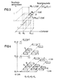
- Coupling elements are provided for adapting the interface between digitally simulated or analogically simulated circuit parts, which carry out a signal transformation between digitally simulated or analogically simulated circuit parts. Each line or signal is implemented separately. Within the model description, the user defines the desired interfaces (possibly by specifying technology parameters). When preparing the simulation, suitable coupling elements are then inserted at all interfaces between analog simulated or digitally simulated circuit parts, which contain the descriptions of the respective conversion functions.
- FIG. 5 shows the insertion of a coupling element KE between a digitally simulated circuit element D and an analogously simulated circuit element A.
- a certain type of coupling element is necessary.
- the two types required are called generators or comparators.
- digital input conditions are applied to a generator at every event.
- Such digital input conditions are state transitions, eg transitions between 1, 0 or X with corresponding signal strengths.
- an analog output signal is generated in this way, which would have been generated by the digitally simulated circuit element D if it had been simulated analog.
- the generator is preferably used as a controllable voltage source E with a controllable internal resistance R ; modeled.
- the voltage E and the internal resistance R result from the digital signal itself, the signal strengths and the technology parameters specified by the user (signal amplitude, potential position, edge steepness).
- FIG. 7 shows the mode of operation of a comparator, that is to say a coupling element for the reverse process of adapting the interface between the output of an analog simulated circuit element and the input of a digitally simulated circuit element.
- the comparator evaluates an analog signal function and generates state transitions, eg transitions between 1, 0 and X and event times when defined comparator thresholds are exceeded or undershot by defined signal strengths.
- the comparator is provided on the input side with a controllable load resistor R L connected in parallel, the resistance value of which results from the signal strengths.
- the comparator thresholds that is to say those analog signal values at which the comparator generates state transitions, are technology-dependent parameters and are specified by the user.
- the output stage described in analog form forms the line termination for the subsequent analog circuit description and at the same time represents the internal resistance of the generator.
- the ideal edges of the digital signal are transformed to standardized edges, which are element-typical (eg power gate) and technology-specific (eg TTL) are.
- the input stage described in analog form forms the line termination for the preceding analog circuit description and at the same time represents the load resistance of the comparator. If the conditions of the comparator points are met, the ideal edge is generated for the respective state transition. Specific comparator thresholds, specific load resistances and possible dependencies on other states must be defined for each state to be evaluated.
- Discrete components or substitute values for the resistance and capacitance coating of connecting lines can be arranged on the connection between a digital element D and an analog element A.
- the coupling elements KE are then always inserted in such a way that the discrete components are always added to the side with an analog description (FIG. 8).
- FIGS. 9 and 10 show the branches typical of a digital-analog transition or an analog-digital transition. Since the analog description always has greater accuracy, the element-related coupling elements are advantageously always arranged such that the analog circuit parts are always "see" the entire pipeline network. This ensures that the analog circuit parts do not behave differently in the simulation in the overall circuit than if the overall circuit were simulated in an analog manner because there is no error with regard to the fan-in or fan-out balance.
Landscapes
- Engineering & Computer Science (AREA)
- Computer Hardware Design (AREA)
- Physics & Mathematics (AREA)
- Theoretical Computer Science (AREA)
- Microelectronics & Electronic Packaging (AREA)
- Evolutionary Computation (AREA)
- Geometry (AREA)
- General Engineering & Computer Science (AREA)
- General Physics & Mathematics (AREA)
- Management, Administration, Business Operations System, And Electronic Commerce (AREA)
Priority Applications (1)
| Application Number | Priority Date | Filing Date | Title |
|---|---|---|---|
| EP90120006A EP0481117A1 (fr) | 1990-10-18 | 1990-10-18 | Méthode pour accélérer la simulation lors de la conception assistée par ordinateur de circuits électroniques et systèmes |
Applications Claiming Priority (1)
| Application Number | Priority Date | Filing Date | Title |
|---|---|---|---|
| EP90120006A EP0481117A1 (fr) | 1990-10-18 | 1990-10-18 | Méthode pour accélérer la simulation lors de la conception assistée par ordinateur de circuits électroniques et systèmes |
Publications (1)
| Publication Number | Publication Date |
|---|---|
| EP0481117A1 true EP0481117A1 (fr) | 1992-04-22 |
Family
ID=8204628
Family Applications (1)
| Application Number | Title | Priority Date | Filing Date |
|---|---|---|---|
| EP90120006A Withdrawn EP0481117A1 (fr) | 1990-10-18 | 1990-10-18 | Méthode pour accélérer la simulation lors de la conception assistée par ordinateur de circuits électroniques et systèmes |
Country Status (1)
| Country | Link |
|---|---|
| EP (1) | EP0481117A1 (fr) |
Cited By (5)
| Publication number | Priority date | Publication date | Assignee | Title |
|---|---|---|---|---|
| EP0855662A1 (fr) | 1997-01-24 | 1998-07-29 | Sgs-Thomson Microelectronics Gmbh | Analyse électrique des circuits integrés |
| EP0986015A1 (fr) * | 1998-09-09 | 2000-03-15 | STMicroelectronics S.r.l. | Procédé pour la simulation dynamique electrique des circuits VLSI |
| DE10043905A1 (de) * | 2000-09-06 | 2002-03-14 | Infineon Technologies Ag | Stromkopplung bei der gemischten Simulation von Schaltungen |
| US6529065B2 (en) | 1999-09-23 | 2003-03-04 | Infineon Technologies Ag | Circuit configuration for controlling the operating point of a power amplifier |
| EP1136898A3 (fr) * | 2000-03-24 | 2004-03-03 | General Electric Company | Processus d'analyse d'ingénieurie intégré avec retour de solution |
Citations (1)
| Publication number | Priority date | Publication date | Assignee | Title |
|---|---|---|---|---|
| EP0381332A2 (fr) * | 1989-02-03 | 1990-08-08 | Texas Instruments Incorporated | Simulation de circuits ayant des parties analogiques et des parties numériques |
-
1990
- 1990-10-18 EP EP90120006A patent/EP0481117A1/fr not_active Withdrawn
Patent Citations (1)
| Publication number | Priority date | Publication date | Assignee | Title |
|---|---|---|---|---|
| EP0381332A2 (fr) * | 1989-02-03 | 1990-08-08 | Texas Instruments Incorporated | Simulation de circuits ayant des parties analogiques et des parties numériques |
Non-Patent Citations (3)
| Title |
|---|
| COMPUTER DESIGN, Band 27, Nr. 3, Februar 1988, Seiten 57-65, Littleton, MA, US; R. GOERING: "A full range of solutions emerge to handle mixed-mode simulation" * |
| IEEE INTERNATIONAL CONFERENCE ON COMPUTER-AIDED DESIGN, ICCCAD-87, Santa Clara, CA, 9. - 12. November 1987, Seiten 488-481; C.M. DYSON et al.: "A pipelined event-driven mixed-mode simulator" * |
| PROCEEDINGS 1988 INTERNATIONAL CONFERENCE ON COMPUTER DESIGN: VLSI IN COMPUTERS AND PROCESSORS, ICCD'88, New York, 3. - 5. Oktober 1988, Seiten 120-123; A.C.J. STROUCKEN et al.: "MILES: A mixed level simulator for analog/digital design" * |
Cited By (7)
| Publication number | Priority date | Publication date | Assignee | Title |
|---|---|---|---|---|
| EP0855662A1 (fr) | 1997-01-24 | 1998-07-29 | Sgs-Thomson Microelectronics Gmbh | Analyse électrique des circuits integrés |
| US6237126B1 (en) | 1997-01-24 | 2001-05-22 | Stmicroelectronics Gmbh | Electrical analysis of integrated circuits |
| EP0986015A1 (fr) * | 1998-09-09 | 2000-03-15 | STMicroelectronics S.r.l. | Procédé pour la simulation dynamique electrique des circuits VLSI |
| US6539346B1 (en) | 1998-09-09 | 2003-03-25 | Stmicroelectronics S.R.L. | Method for the electric dynamic simulation of VLSI circuits |
| US6529065B2 (en) | 1999-09-23 | 2003-03-04 | Infineon Technologies Ag | Circuit configuration for controlling the operating point of a power amplifier |
| EP1136898A3 (fr) * | 2000-03-24 | 2004-03-03 | General Electric Company | Processus d'analyse d'ingénieurie intégré avec retour de solution |
| DE10043905A1 (de) * | 2000-09-06 | 2002-03-14 | Infineon Technologies Ag | Stromkopplung bei der gemischten Simulation von Schaltungen |
Similar Documents
| Publication | Publication Date | Title |
|---|---|---|
| DE69838835T2 (de) | Verfahren zur Prüfung und zur Darstellung einer Hardware durch Zerlegung und Aufteilung | |
| DE69616416T2 (de) | Verfahren zur Simulation einer Schaltung | |
| DE60005670T2 (de) | Aktualisierung der platzierung während der technologieabbildung | |
| DE69225527T2 (de) | Verfahren und System zur automatischen Bestimmung der logischen Funktion einer Schaltung | |
| DE69326072T2 (de) | Verfahren zur Prüfung eines sequentiellen endlichen Automaten | |
| EP0580663B1 (fr) | Procede pour la verification de systemes traitant des donnees | |
| WO2000026824A1 (fr) | Procede et dispositif pour la comparaison d'une premiere caracteristique avec des caracteristiques predeterminees d'un systeme technique | |
| DE10043905A1 (de) | Stromkopplung bei der gemischten Simulation von Schaltungen | |
| DE102004036813A1 (de) | Verfahren zum Erzeugen eines Schaltungsmodells | |
| Bandler et al. | Yield-driven electromagnetic optimization via multilevel multidimensional models | |
| EP1062604B1 (fr) | Procede et dispositif pour determiner une defaillance d'un systeme technique | |
| EP0481117A1 (fr) | Méthode pour accélérer la simulation lors de la conception assistée par ordinateur de circuits électroniques et systèmes | |
| Hui et al. | Discrete transform technique for solving coupled integro-differential equations in digital computers | |
| DE19626984C1 (de) | Verfahren zur rechnergestützten Ermittlung einer Systemzusammenhangsfunktion | |
| EP1061464A1 (fr) | Classification de variables dans un système d'équations simultanées décrit par des langages de description de matériel | |
| Zhou et al. | A distributed-RCL model for MCM layout | |
| DE69524721T2 (de) | Signalgenerator zur modellierung des dynamischen verhaltens eines systems | |
| DE69811469T2 (de) | Verfahren zur Leistungsbewertung von VLSI-Schaltungen | |
| DE10200833A1 (de) | Gerät und Verfahren für eine Teststimuliverdichtung | |
| Striebel et al. | A charge oriented mixed multirate method for a special class of index-1 network equations in chip design | |
| Tyssedal et al. | Autoregressive processes with a time dependent variance | |
| Lin et al. | Signal delay in general RC networks with application to timing simulation of digital integrated circuits | |
| EP1068580B1 (fr) | Procede de comparaison de circuits electriques | |
| Zhou et al. | A fast wavelet collocation method for high-speed VLSI circuit simulation | |
| Dacka | On the controllability of nonlinear systems with time-variable delays |
Legal Events
| Date | Code | Title | Description |
|---|---|---|---|
| PUAI | Public reference made under article 153(3) epc to a published international application that has entered the european phase |
Free format text: ORIGINAL CODE: 0009012 |
|
| 17P | Request for examination filed |
Effective date: 19901205 |
|
| AK | Designated contracting states |
Kind code of ref document: A1 Designated state(s): AT BE CH DE DK ES FR GB GR IT LI LU NL SE |
|
| STAA | Information on the status of an ep patent application or granted ep patent |
Free format text: STATUS: THE APPLICATION HAS BEEN WITHDRAWN |
|
| RBV | Designated contracting states (corrected) |
Designated state(s): DE FR GB IT NL |
|
| 18W | Application withdrawn |
Withdrawal date: 19920509 |
|
| R18W | Application withdrawn (corrected) |
Effective date: 19920509 |