EP0381448A2 - Vorrichtung und Verfahren zum Frequenzwechsel - Google Patents
Vorrichtung und Verfahren zum Frequenzwechsel Download PDFInfo
- Publication number
- EP0381448A2 EP0381448A2 EP90300956A EP90300956A EP0381448A2 EP 0381448 A2 EP0381448 A2 EP 0381448A2 EP 90300956 A EP90300956 A EP 90300956A EP 90300956 A EP90300956 A EP 90300956A EP 0381448 A2 EP0381448 A2 EP 0381448A2
- Authority
- EP
- European Patent Office
- Prior art keywords
- microprocessor
- frequency
- memory
- frequencies
- coupled
- Prior art date
- Legal status (The legal status is an assumption and is not a legal conclusion. Google has not performed a legal analysis and makes no representation as to the accuracy of the status listed.)
- Granted
Links
Images


Classifications
-
- G—PHYSICS
- G06—COMPUTING OR CALCULATING; COUNTING
- G06F—ELECTRIC DIGITAL DATA PROCESSING
- G06F1/00—Details not covered by groups G06F3/00 - G06F13/00 and G06F21/00
- G06F1/04—Generating or distributing clock signals or signals derived directly therefrom
- G06F1/08—Clock generators with changeable or programmable clock frequency
-
- G—PHYSICS
- G01—MEASURING; TESTING
- G01R—MEASURING ELECTRIC VARIABLES; MEASURING MAGNETIC VARIABLES
- G01R31/00—Arrangements for testing electric properties; Arrangements for locating electric faults; Arrangements for electrical testing characterised by what is being tested not provided for elsewhere
- G01R31/28—Testing of electronic circuits, e.g. by signal tracer
- G01R31/317—Testing of digital circuits
- G01R31/3181—Functional testing
- G01R31/319—Tester hardware, i.e. output processing circuits
- G01R31/31917—Stimuli generation or application of test patterns to the device under test [DUT]
Definitions
- frequency control apparatus for providing a selected one of two frequencies to a microprocessor, characterized by: first frequency generating means capable of generating a signal having a first frequency; second frequency generating means capable of generating a signal having a second frequency; a microprocessor to which signals of said first frequency or said second frequency are selectively applied; logic circuit means adapted to selectively gate a signal from either said first frequency generating means or said second frequency generating means to said microprocessor; flip-flop means adapted to control said logic circuit means and having a data input coupled to an output of said microprocessor; address decoder means controlled by said microprocessor and coupled to a clock input of said flip-flop means; memory means coupled to said microprocessor to provide data to said microprocessor for control thereof; and reset means controlled by said address decoder means and coupled to said microprocessor for resetting said microprocessor.
- a process for providing a selected one of two different frequencies from two frequency generating means through logic means to a microprocessor having memory means characterized by the following steps: (a) determining whether a data pattern in the microprocessor memory is identical to a first reference pattern associated with a first of two frequencies; (b) if said patterns are identical, controlling said logic means to cause a first of the two frequencies to be provided to the microprocessor from a first frequency generating means; (c) if said patterns are not identical, determining whether the data pattern in the microprocessor memory is identical to a second reference pattern associated with a second of the two frequencies; (d) if said data pattern and said second reference pattern are identical, controlling said logic means to cause a second of the two frequencies to be provided to the microprocessor from a second frequency generating means; (e) if said data pattern and said second reference pattern are not identical, determining which of the two frequencies is required; (f) writing a reference pattern associated with the selected one of the two frequencies
- the apparatus and method for changing frequencies of the present invention are capable of being used in a number of different applications.
- One such application is in a testing device which may be used in testing various elements of a data processing system. It is common for the owner of such a system to select various elements of the system from different manufacturers in order to achieve the precise combination desired.
- a first type of business terminal employed in such a system might be purchased from one manufacturer, while a second type of business terminal might be purchased from a second manufacturer. It is entirely possible that these two terminals would operate on different basic frequencies.
- test device can provide the necessary plurality of frequencies.
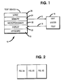
- a test device 10 is coupled by paths 12 and 14 to a unit under test 16.
- the test device 10 may include a keyboard 18, a display 20, a microprocessor 22, a memory 24 and appropriate logic circuitry 26.
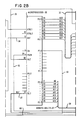
- Figs. 2A, 2B and 2C when combined in the manner depicted in Fig. 2, is a circuit comprising those elements of the test device 10 which cooperate to provide the plurality of frequencies desired, and to further provide the capability for changing from one frequency to another. Included in these elements is a microprocessor 30, which may be of type 80C31, manufactured by Intel Corporation, Santa Clara, California.
- Positions P0.0-P0.7 inclusive of the microprocessor 30 are coupled by a data address bus 32 to positions D1-D8 inclusive of an address latch 34, which may be of type 74HC373, manufactured by Texas Instruments Incorporated, Dallas, Texas, and to positions 00-07 of a memory such as a read-only memory (ROM) 36 which may be of type I2764 manufactured by Intel Corporation.
- the address latch 34 is used to hold the least significant eight bits of the address for the ROM 36. These bits are stored in a first cycle of the microprocessor 30 and are combined in a subsequent cycle with the remaining necessary address bits, which are provided by positions P2.0-P2.4 of the microprocessor 30.
- Position ALE of the microprocessor 30 is connected by a conductor 33 to position CEN of the address latch 34.
- Position PSEN of the microprocessor 30 is connected by a conductor 35 to position OE of the ROM avoid the inconvenience and expense of having to employ a number of different testing devices. Since various elements of the system may require the application of different frequencies for the necessary testing, it is advantageous if the test device can provide the necessary plurality of frequencies.
- a test device 10 is coupled by paths 12 and 14 to a unit under test 16.
- the test device 10 may include a keyboard 18, a display 20, a microprocessor 22, a memory 24 and appropriate logic circuitry 26.
- Figs. 2A, 2B and 2C when combined in the manner depicted in Fig. 2, is a circuit comprising those elements of the test device 10 which cooperate to provide the plurality of frequencies desired, and to further provide the capability for changing from one frequency to another. Included in these elements is a microprocessor 30, which may be of type 80C31, manufactured by Intel Corporation, Santa Clara, California.
- Positions P0.0-P0.7 inclusive of the microprocessor 30 are coupled by a data address bus 32 to positions D1-D8 inclusive of an address latch 34, which may be of type 74HC373, manufactured by Texas Instruments Incorporated, Dallas, Texas, and to positions 00-07 of a memory such as a read-only memory (ROM) 36 which may be of type I2764 manufactured by Intel Corporation.
- the address latch 34 is used to hold the least significant eight bits of the address for the ROM 36. These bits are stored in a first cycle of the microprocessor 30 and are combined in a subsequent cycle with the remaining necessary address bits, which are provided by positions P2.0-P2.4 of the microprocessor 30.
- Position ALE of the microprocessor 30 is connected by a conductor 33 to position CEN of the address latch 34.
- Position PSEN of the microprocessor 30 is connected by a conductor 35 to position OE of the ROM 36.
- Positions Q1-Q8 inclusive of the address latch 34 are coupled to address positions A0-A7 inclusive of the ROM 36 and positions P2.0-P2.4 of the microprocessor 30 are coupled to positions A8-A12 of the ROM 36 by means of an address bus 38.
- Positions 00-07 of the ROM 36 are coupled via the data address bus 32 to positions P0.0-P0.7 of the microprocessor 30.
- Positions P2.4-P2.7 of the microprocessor 30 are coupled by the address bus 38 to positions A, B, C and G1 of an address decoder 40, which may be of type 74LS138, manufactured by Texas Instruments Incorporated.
- Position P3.7 of the microprocessor 30 is connected by a conductor 37 to position G2A of the address decoder 40.
- the two basic frequencies to be provided by the test device 10 are generated, in the illustrated embodiment, by two crystal oscillators X1 and X2 (Fig. 2A).
- oscillator X1 provides a frequency of 14.7456 MHZ and oscillator X2 provides a frequency of 12.000 MHZ.
- different types of frequency generators could be employed and different frequencies could be provided.
- Each of the crystal oscillators X1 and X2 is connected at one side to a source of potential designated V CC and to ground through pin 7.
- the other side of the oscillator X1 is connected to one input of a NOR gate 48, which may be of type 74HC02, manufactured by Texas Instruments Incorporated.
- the other side of the oscillator X2 is also connected to one input of a NOR gate 46, which may also be of type 74HC02.
- the outputs of the NOR gates 46 and 48 are connected to the inputs of a two-input NOR gate 50, which may also be of type 74HC02.
- the output of the NOR gate 50 is connected to the XTAL1 position of the microprocessor 30.
- the other inputs of the NOR gates 46 and 48 are connected, respectively, to the Q and Q/ outputs of a flip-flop 52, which may be of type 74HC74, manufactured by Texas Instruments Incorporated.
- the PRE and CLR inputs of the flip-flop 52 are connected through nodes 54 and 56 to the potential source V CC .
- the clock input of said flip-flop is connected through a node 57, a 4,700-ohm resistor 58 and the node 54 to the source V CC , and is also connected through the node 57 and a conductor 60 to a node 82, which in turn is connected to one input of a NOR gate 80, which may be of type 74HC02.
- the node 82 is also connected by the conductor 60 to the output of an inverter 62 (Fig. 2C), which may be of type 7406, manufactured by Texas Instruments Incorporated, having its input connected in turn to position Y3 of the address decoder 40.
- the D input of the flip-flop 52 is connected by a conductor 53 to an output position P1.0 of the microprocessor 30.
- a second input of the NOR gate 80 is connected via a conductor 66 to a node 68.
- a 10-microfarad capacitor 70 is connected between the node 68 and the node 56, to which is connected the potential source V CC .
- a further branch from the node 68 extends through an 8,200-ohm resistor 72 and a node 74 to a ground connection.
- a diode 76 connects the node 74 to a node 78 on the conductor 66.
- the node 78 is connected to one input of a NOR gate 80, which may be of type 74HC02.
- the other input of the NOR gate 80 is connected by a node 82 on the conductor 60 to the output of the inverter 62 (Fig. 2C).
- the output of the NOR gate 80 is connected to the TR input of a timer 84, which may be of type LM555, manufactured by Texas Instruments Incorporated, and which is configured as a monostable multivibrator.
- the CV input of the timer 84 is connected through a 0.01-microfarad capacitor 86 to ground.
- the R input of the timer 84 is connected through a node 88 to the potential source V CC .
- a path extends from the node 88 through a one-megohm resistor 90, two nodes 92 and 94, and a 0.047-microfarad capacitor 96 to ground.
- the nodes 92 and 94 are connected, respectively, to the DIS and THR positions of the timer 84.
- the Q output of the timer 84 is connected by a conductor 98 to the reset position RST of the microprocessor 30.
- the operation of the circuit of Figs. 2A-2C inclusive is as follows. Upon initial power-up of the circuit, the outputs of the flip-flop 52 are in a random order. If the Q output of the flip-flop 52 and the input of corresponding NOR gate 46 are in a high state (+5 volts), the oscillator X2 is disabled because the output of NOR gate 46 assumes a low level (0 volts). The Q/ output of the flip-flop 52 and the corresponding input of NOR gate 48 will then have a low level. Because of the low level on said input of NOR gate 48, the oscillator X1 is enabled and the signal from said oscillator is passed through the NOR gate 50 and is applied to the XTAL1 input of the microprocessor 30. If the output levels of the flip-flop 52 were reversed at the time of power-up of the circuit, then the oscillator X2 would be enabled and the oscillator X1 would be disabled.
- NOR gate 80 On the same power-up sequence, a high level is present at the input of NOR gate 80 which is connected to node 78 because of the RC time constant of the resistor 72 and the capacitor 70. As time passes (approximately 100 milliseconds with the values shown), the voltage level at said input of the NOR gate 80 will fall to zero volts. However, at the time that said input of the gate 80 is at a high level, the output of the gate 80 is at a low level.
- This low level signal is applied to the TR position of the timer 84, and causes the Q output of said timer to go to a high level for the time specified by the RC time constant of resistor 90 and capacitor 96 (approximately 50 milliseconds for the values shown), and then to return to a low level.
- This high-level pulse is applied over conductor 98 to the RST position of the microprocessor 30 and causes said microprocessor to be reset.
- the random access memory contained therein has random data written throughout it.
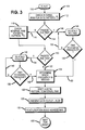
- the firmware program contained in the ROM 36 causes the system to perform a routine that first checks the contents of the random access memory (RAM) of the microprocessor 30 against specific byte patterns representing the available frequencies as generated by the oscillators X1 and X2.
- This routine or program 108 commences from a start condition, represented by block 110.
- the internal RAM of microprocessor 30 is checked to see if its contents match byte pattern no. 1 stored in ROM 36, corresponding to oscillator X1, and a determination is made (decision block 114) as to whether such a match exists. Since the data stored in the RAM at this point is random, because this is the initial power-up of the unit, and not a self-induced reset, the test will not be passed, and the process continues over path 116 to block 118, in which the internal RAM is checked to see if its contents match byte pattern no.
- the determination as to desired frequency referred to in block 124 may be made in any one of several ways. For example, this could be accomplished by elements of the system in accordance with an overall testing program, or could be accomplished by a human operator in response to a "display prompt" appearing on the screen of the test device 10. Such a "display prompt” could take the form of a message on the screen instructing the operator to the effect that if the terminal being tested is "brand A", to depress the "zero” key on the keyboard 18, and if the terminal being tested is "brand B", to depress the "one” key on the keyboard 18. The appropriate frequency for the indicated brand of terminal would then be selected.
- the first step in causing the microprocessor 30 to be provided with the desired frequency is to cause the appropriate byte pattern (in this case, byte pattern no. 2) to be written from the ROM 36 to the internal RAM, as indicated in block 126.
- the microprocessor 30 is then caused to provide a low level signal from position P1.0 via the conductor 53 to the D position of the flip-flop 52, as represented by block 128.
- the microprocessor 30 fetches the next instruction from the ROM 36, which tells the microprocessor to do an external read operation at location B000, as represented in block 130. This means that positions P2.4-P2.7 of the microprocessor are set. These signals are carried over address bus 38 to positions A, B, C and G1 in the address decoder 40.
- the microprocessor 30 then causes a low-level pulse of approximately 400-500 nanoseconds to appear at position P3.7.
- This pulse is carried over conductor 37 to position G2A of the address decoder 40, which in turn causes a low-level pulse of approximately 400-500 nanoseconds duration to occur at position 12 of the address decoder 40 and at the input of the inverter 62.
- This pulse is inverted by the inverter 62 and is carried over the conductor 60 and the node 82 to an input of the gate 80 and over the node 57 to the CLK input of the flip-flop 52.
- the flip-flop 52 On the rising edge of this pulse, applied to the CLK input, the flip-flop 52 provides a low level Q output and a high-level Q/ output.
- the process continues to block 132 where an instruction in the ROM 36 causes the microprocessor 30 to remain in an infinite loop routine, to await a reset operation.
- the high level on the input of the NOR gate 80 causes a low level signal to be applied to the TR position of the timer 84, which in turn causes another reset pulse to be transmitted via the conductor 98 to the RST position of the microprocessor 30, so that the microprocessor then goes through another reset sequence.
- the program 108 then returns to the start block 110, where a check is again made of the internal RAM for byte pattern no. 1 (block 112). Since the internal RAM now contains byte pattern no. 2, this test is not passed (block 114) and the program continues to block 118, where the internal RAM contents are compared with byte pattern no. 2. This time, the test is passed (block 120), and the program continues over path 134 to block 136, in which the program routine associated with the selected frequency is performed. At the completion of performance of that routine, an inquiry is made (block 138) as to whether the frequency should be changed. This can be determined by the human operator or by a controlling program. If the frequency is not to be changed, the program returns over path 140 and the routine is repeated. If the frequency is to be changed, the program continues over path 142 to the previously-discussed block 124.
- CMOS parts have been used in the circuit of Figs. 2A-2C
- other types of circuitry such as TTL circuitry
- a microprocessor of type 8031 manufactured by Intel Corporation
- the output of the NOR gate 50 would be connected to the XTAL2 position of the microprocessor of type 8031, and the XTAL1 position of said microprocessor would be connected to ground.
- oscillators with frequencies other than the values given above can be used so long as the frequency does not exceed the maximum frequency specification of the microprocessor 30 or the gates 46, 48 and 50.
Landscapes
- Engineering & Computer Science (AREA)
- Theoretical Computer Science (AREA)
- Physics & Mathematics (AREA)
- General Engineering & Computer Science (AREA)
- General Physics & Mathematics (AREA)
- Tests Of Electronic Circuits (AREA)
- Test And Diagnosis Of Digital Computers (AREA)
- Stabilization Of Oscillater, Synchronisation, Frequency Synthesizers (AREA)
Applications Claiming Priority (2)
| Application Number | Priority Date | Filing Date | Title |
|---|---|---|---|
| US07/304,050 US4958309A (en) | 1989-01-30 | 1989-01-30 | Apparatus and method for changing frequencies |
| US304050 | 1994-09-12 |
Publications (3)
| Publication Number | Publication Date |
|---|---|
| EP0381448A2 true EP0381448A2 (de) | 1990-08-08 |
| EP0381448A3 EP0381448A3 (de) | 1991-12-04 |
| EP0381448B1 EP0381448B1 (de) | 1996-06-26 |
Family
ID=23174840
Family Applications (1)
| Application Number | Title | Priority Date | Filing Date |
|---|---|---|---|
| EP90300956A Expired - Lifetime EP0381448B1 (de) | 1989-01-30 | 1990-01-30 | Vorrichtung und Verfahren zum Frequenzwechsel |
Country Status (4)
| Country | Link |
|---|---|
| US (1) | US4958309A (de) |
| EP (1) | EP0381448B1 (de) |
| JP (1) | JPH02240711A (de) |
| DE (1) | DE69027545T2 (de) |
Cited By (6)
| Publication number | Priority date | Publication date | Assignee | Title |
|---|---|---|---|---|
| EP0510241A3 (en) * | 1991-04-22 | 1993-01-13 | Acer Incorporated | Upgradeable/downgradeable computer |
| US5455927A (en) * | 1991-08-22 | 1995-10-03 | Acer Incorporated | Dual socket upgradeable computer motherboard with automatic detection and enablement of inserted upgrade CPU chip |
| US5490279A (en) * | 1993-05-21 | 1996-02-06 | Intel Corporation | Method and apparatus for operating a single CPU computer system as a multiprocessor system |
| US5551012A (en) * | 1991-04-22 | 1996-08-27 | Acer Incorporated | Single socket upgradeable computer motherboard with automatic detection and socket reconfiguration for inserted CPU chip |
| US5761479A (en) * | 1991-04-22 | 1998-06-02 | Acer Incorporated | Upgradeable/downgradeable central processing unit chip computer systems |
| US5931930A (en) * | 1994-06-29 | 1999-08-03 | Intel Corporation | Processor that indicates system bus ownership in an upgradable multiprocessor computer system |
Families Citing this family (3)
| Publication number | Priority date | Publication date | Assignee | Title |
|---|---|---|---|---|
| US5197126A (en) * | 1988-09-15 | 1993-03-23 | Silicon Graphics, Inc. | Clock switching circuit for asynchronous clocks of graphics generation apparatus |
| US5485594A (en) * | 1992-07-17 | 1996-01-16 | International Business Machines Corporation | Apparatus and method using an atomic fetch and add for establishing temporary ownership of a common system resource in a multiprocessor data processing system |
| US5513152A (en) * | 1994-06-22 | 1996-04-30 | At&T Global Information Solutions Company | Circuit and method for determining the operating performance of an integrated circuit |
Family Cites Families (16)
| Publication number | Priority date | Publication date | Assignee | Title |
|---|---|---|---|---|
| NL7207216A (de) * | 1972-05-27 | 1973-11-29 | ||
| US3980993A (en) * | 1974-10-17 | 1976-09-14 | Burroughs Corporation | High-speed/low-speed interface for data processing systems |
| US4050096A (en) * | 1974-10-30 | 1977-09-20 | Motorola, Inc. | Pulse expanding system for microprocessor systems with slow memory |
| JPS5266346A (en) * | 1975-11-29 | 1977-06-01 | Tokyo Electric Co Ltd | Synch. clock control of microcomputer system |
| GB1561961A (en) * | 1977-04-20 | 1980-03-05 | Int Computers Ltd | Data processing units |
| US4191998A (en) * | 1978-03-29 | 1980-03-04 | Honeywell Inc. | Variable symmetry multiphase clock generator |
| US4254475A (en) * | 1979-03-12 | 1981-03-03 | Raytheon Company | Microprocessor having dual frequency clock |
| US4458308A (en) * | 1980-10-06 | 1984-07-03 | Honeywell Information Systems Inc. | Microprocessor controlled communications controller having a stretched clock cycle |
| JPS57101957A (en) * | 1980-12-17 | 1982-06-24 | Hitachi Ltd | Storage control device |
| US4398155A (en) * | 1981-06-15 | 1983-08-09 | Motorola, Inc. | Multiple clock switching circuit |
| US4509120A (en) * | 1982-09-30 | 1985-04-02 | Bell Telephone Laboratories, Inc. | Variable cycle-time microcomputer |
| US4748417A (en) * | 1985-02-05 | 1988-05-31 | Siemens Aktiengesellschaft | Method and circuit arrangement for switching a clock-controlled device having a plurality of operating statuses |
| JPS62166419A (ja) * | 1986-01-17 | 1987-07-22 | インタ−ナショナル ビジネス マシ−ンズ コ−ポレ−ション | 多周波クロック発生装置 |
| US4837764A (en) * | 1987-03-26 | 1989-06-06 | Bunker Ramo Corporation | Programmable apparatus and method for testing computer peripherals |
| US4813005A (en) * | 1987-06-24 | 1989-03-14 | Hewlett-Packard Company | Device for synchronizing the output pulses of a circuit with an input clock |
| US4855616A (en) * | 1987-12-22 | 1989-08-08 | Amdahl Corporation | Apparatus for synchronously switching frequency source |
-
1989
- 1989-01-30 US US07/304,050 patent/US4958309A/en not_active Expired - Lifetime
-
1990
- 1990-01-26 JP JP2015167A patent/JPH02240711A/ja active Pending
- 1990-01-30 EP EP90300956A patent/EP0381448B1/de not_active Expired - Lifetime
- 1990-01-30 DE DE69027545T patent/DE69027545T2/de not_active Expired - Fee Related
Cited By (7)
| Publication number | Priority date | Publication date | Assignee | Title |
|---|---|---|---|---|
| EP0510241A3 (en) * | 1991-04-22 | 1993-01-13 | Acer Incorporated | Upgradeable/downgradeable computer |
| US5546563A (en) * | 1991-04-22 | 1996-08-13 | Acer Incorporated | Single chip replacement upgradeable computer motherboard with enablement of inserted upgrade CPU chip |
| US5551012A (en) * | 1991-04-22 | 1996-08-27 | Acer Incorporated | Single socket upgradeable computer motherboard with automatic detection and socket reconfiguration for inserted CPU chip |
| US5761479A (en) * | 1991-04-22 | 1998-06-02 | Acer Incorporated | Upgradeable/downgradeable central processing unit chip computer systems |
| US5455927A (en) * | 1991-08-22 | 1995-10-03 | Acer Incorporated | Dual socket upgradeable computer motherboard with automatic detection and enablement of inserted upgrade CPU chip |
| US5490279A (en) * | 1993-05-21 | 1996-02-06 | Intel Corporation | Method and apparatus for operating a single CPU computer system as a multiprocessor system |
| US5931930A (en) * | 1994-06-29 | 1999-08-03 | Intel Corporation | Processor that indicates system bus ownership in an upgradable multiprocessor computer system |
Also Published As
| Publication number | Publication date |
|---|---|
| DE69027545T2 (de) | 1997-01-23 |
| EP0381448A3 (de) | 1991-12-04 |
| EP0381448B1 (de) | 1996-06-26 |
| US4958309A (en) | 1990-09-18 |
| DE69027545D1 (de) | 1996-08-01 |
| JPH02240711A (ja) | 1990-09-25 |
Similar Documents
| Publication | Publication Date | Title |
|---|---|---|
| US4433413A (en) | Built-in apparatus and method for testing a microprocessor system | |
| US4785416A (en) | Microprocessor timing emulator having a "Wait" state | |
| US5291495A (en) | Method for designing a scan path for a logic circuit and testing of the same | |
| US3470542A (en) | Modular system design | |
| EP0135864A2 (de) | System und Verfahren zum automatischen Prüfen von in integrierter Schaltung aufgebauter Speichermatrix auf verschiedenen Speichermatrixprüfern | |
| EP0381448B1 (de) | Vorrichtung und Verfahren zum Frequenzwechsel | |
| US4922445A (en) | Logic circuit simulation method | |
| JP2002123562A (ja) | テスタ構築データの生成方法およびテスタの構築方法並びにテスト回路 | |
| US4611281A (en) | Apparatus for analyzing microprocessor operation | |
| JP2540069B2 (ja) | ユ―ザ・インタフェ―ス装置 | |
| JP2001101017A (ja) | 追加のハードウェア無しにpcカード上のfpgaをプログラムする方法及びシステム | |
| EP0303662A1 (de) | Dynamisches testverfahren für eine ausrüstung | |
| JPH04215316A (ja) | 逐次有限状態マシン回路とそのような回路を具える集積回路 | |
| KR19980064006A (ko) | 범용 입력 데이터 샘플링장치 및 방법 | |
| EP0166575A2 (de) | System für die Prüfung funktioneller elektronischer Schaltungen | |
| US6237117B1 (en) | Method for testing circuit design using exhaustive test vector sequence | |
| EP0363465B1 (de) | GERäT ZUR RECHNERGESTÜTZEN ERZEUGUNG VON PRÜFPROGRAMMEN FÜR DIGITALE SCHALTUNGEN | |
| JPH085714A (ja) | 集積回路検査方法及び集積回路配置 | |
| KR100263030B1 (ko) | 중앙처리장치 구동 주파수 자동 선택 장치 및 그 제어방법 | |
| GB2099618A (en) | Algorithmic word generator | |
| EP0166220A2 (de) | Digitaldatenverarbeitungseinrichtung mit Adressenzuordnungsvorrichtung | |
| US5910901A (en) | Logic simulator | |
| EP0135009A2 (de) | Die Erfindung bezieht sich auf eine Anordnung und ein Verfahren zum Prüfen eines Mikroprozessorsystem | |
| JP2824853B2 (ja) | パターンデータ書込み方式 | |
| KR200153410Y1 (ko) | 테스트 메시지 출력장치 |
Legal Events
| Date | Code | Title | Description |
|---|---|---|---|
| PUAI | Public reference made under article 153(3) epc to a published international application that has entered the european phase |
Free format text: ORIGINAL CODE: 0009012 |
|
| AK | Designated contracting states |
Kind code of ref document: A2 Designated state(s): DE FR GB |
|
| PUAL | Search report despatched |
Free format text: ORIGINAL CODE: 0009013 |
|
| AK | Designated contracting states |
Kind code of ref document: A3 Designated state(s): DE FR GB |
|
| 17P | Request for examination filed |
Effective date: 19920513 |
|
| RAP1 | Party data changed (applicant data changed or rights of an application transferred) |
Owner name: NCR INTERNATIONAL INC. |
|
| RAP1 | Party data changed (applicant data changed or rights of an application transferred) |
Owner name: AT&T GLOBAL INFORMATION SOLUTIONS INTERNATIONAL IN |
|
| 17Q | First examination report despatched |
Effective date: 19950718 |
|
| GRAH | Despatch of communication of intention to grant a patent |
Free format text: ORIGINAL CODE: EPIDOS IGRA |
|
| GRAH | Despatch of communication of intention to grant a patent |
Free format text: ORIGINAL CODE: EPIDOS IGRA |
|
| RAP1 | Party data changed (applicant data changed or rights of an application transferred) |
Owner name: NCR INTERNATIONAL INC. |
|
| GRAA | (expected) grant |
Free format text: ORIGINAL CODE: 0009210 |
|
| AK | Designated contracting states |
Kind code of ref document: B1 Designated state(s): DE FR GB |
|
| REF | Corresponds to: |
Ref document number: 69027545 Country of ref document: DE Date of ref document: 19960801 |
|
| ET | Fr: translation filed | ||
| PLBE | No opposition filed within time limit |
Free format text: ORIGINAL CODE: 0009261 |
|
| STAA | Information on the status of an ep patent application or granted ep patent |
Free format text: STATUS: NO OPPOSITION FILED WITHIN TIME LIMIT |
|
| 26N | No opposition filed | ||
| PGFP | Annual fee paid to national office [announced via postgrant information from national office to epo] |
Ref country code: GB Payment date: 19990108 Year of fee payment: 10 |
|
| PGFP | Annual fee paid to national office [announced via postgrant information from national office to epo] |
Ref country code: FR Payment date: 19990112 Year of fee payment: 10 |
|
| PGFP | Annual fee paid to national office [announced via postgrant information from national office to epo] |
Ref country code: DE Payment date: 19990127 Year of fee payment: 10 |
|
| PG25 | Lapsed in a contracting state [announced via postgrant information from national office to epo] |
Ref country code: GB Free format text: LAPSE BECAUSE OF NON-PAYMENT OF DUE FEES Effective date: 20000130 |
|
| GBPC | Gb: european patent ceased through non-payment of renewal fee |
Effective date: 20000130 |
|
| PG25 | Lapsed in a contracting state [announced via postgrant information from national office to epo] |
Ref country code: FR Free format text: LAPSE BECAUSE OF NON-PAYMENT OF DUE FEES Effective date: 20000929 |
|
| PG25 | Lapsed in a contracting state [announced via postgrant information from national office to epo] |
Ref country code: DE Free format text: LAPSE BECAUSE OF NON-PAYMENT OF DUE FEES Effective date: 20001101 |
|
| REG | Reference to a national code |
Ref country code: FR Ref legal event code: ST |