EP0382929A2 - Spannungsreglerschaltung - Google Patents
Spannungsreglerschaltung Download PDFInfo
- Publication number
- EP0382929A2 EP0382929A2 EP89123228A EP89123228A EP0382929A2 EP 0382929 A2 EP0382929 A2 EP 0382929A2 EP 89123228 A EP89123228 A EP 89123228A EP 89123228 A EP89123228 A EP 89123228A EP 0382929 A2 EP0382929 A2 EP 0382929A2
- Authority
- EP
- European Patent Office
- Prior art keywords
- voltage
- voltage regulator
- channel mos
- regulator circuit
- charge pump
- Prior art date
- Legal status (The legal status is an assumption and is not a legal conclusion. Google has not performed a legal analysis and makes no representation as to the accuracy of the status listed.)
- Granted
Links
Images


Classifications
-
- G—PHYSICS
- G05—CONTROLLING; REGULATING
- G05F—SYSTEMS FOR REGULATING ELECTRIC OR MAGNETIC VARIABLES
- G05F3/00—Non-retroactive systems for regulating electric variables by using an uncontrolled element, or an uncontrolled combination of elements, such element or such combination having self-regulating properties
- G05F3/02—Regulating voltage or current
- G05F3/08—Regulating voltage or current wherein the variable is DC
- G05F3/10—Regulating voltage or current wherein the variable is DC using uncontrolled devices with non-linear characteristics
- G05F3/16—Regulating voltage or current wherein the variable is DC using uncontrolled devices with non-linear characteristics being semiconductor devices
- G05F3/20—Regulating voltage or current wherein the variable is DC using uncontrolled devices with non-linear characteristics being semiconductor devices using diode- transistor combinations
- G05F3/205—Substrate bias-voltage generators
-
- G—PHYSICS
- G11—INFORMATION STORAGE
- G11C—STATIC STORES
- G11C5/00—Details of stores covered by group G11C11/00
- G11C5/14—Power supply arrangements, e.g. power down, chip selection or deselection, layout of wirings or power grids, or multiple supply levels
- G11C5/147—Voltage reference generators, voltage or current regulators; Internally lowered supply levels; Compensation for voltage drops
-
- G—PHYSICS
- G05—CONTROLLING; REGULATING
- G05F—SYSTEMS FOR REGULATING ELECTRIC OR MAGNETIC VARIABLES
- G05F3/00—Non-retroactive systems for regulating electric variables by using an uncontrolled element, or an uncontrolled combination of elements, such element or such combination having self-regulating properties
- G05F3/02—Regulating voltage or current
- G05F3/08—Regulating voltage or current wherein the variable is DC
- G05F3/10—Regulating voltage or current wherein the variable is DC using uncontrolled devices with non-linear characteristics
- G05F3/16—Regulating voltage or current wherein the variable is DC using uncontrolled devices with non-linear characteristics being semiconductor devices
- G05F3/20—Regulating voltage or current wherein the variable is DC using uncontrolled devices with non-linear characteristics being semiconductor devices using diode- transistor combinations
- G05F3/24—Regulating voltage or current wherein the variable is DC using uncontrolled devices with non-linear characteristics being semiconductor devices using diode- transistor combinations wherein the transistors are of the field-effect type only
-
- G—PHYSICS
- G11—INFORMATION STORAGE
- G11C—STATIC STORES
- G11C16/00—Erasable programmable read-only memories
- G11C16/02—Erasable programmable read-only memories electrically programmable
- G11C16/06—Auxiliary circuits, e.g. for writing into memory
- G11C16/30—Power supply circuits
-
- G—PHYSICS
- G11—INFORMATION STORAGE
- G11C—STATIC STORES
- G11C5/00—Details of stores covered by group G11C11/00
- G11C5/14—Power supply arrangements, e.g. power down, chip selection or deselection, layout of wirings or power grids, or multiple supply levels
- G11C5/145—Applications of charge pumps; Boosted voltage circuits; Clamp circuits therefor
-
- H—ELECTRICITY
- H02—GENERATION; CONVERSION OR DISTRIBUTION OF ELECTRIC POWER
- H02M—APPARATUS FOR CONVERSION BETWEEN AC AND AC, BETWEEN AC AND DC, OR BETWEEN DC AND DC, AND FOR USE WITH MAINS OR SIMILAR POWER SUPPLY SYSTEMS; CONVERSION OF DC OR AC INPUT POWER INTO SURGE OUTPUT POWER; CONTROL OR REGULATION THEREOF
- H02M3/00—Conversion of DC power input into DC power output
- H02M3/02—Conversion of DC power input into DC power output without intermediate conversion into AC
- H02M3/04—Conversion of DC power input into DC power output without intermediate conversion into AC by static converters
- H02M3/06—Conversion of DC power input into DC power output without intermediate conversion into AC by static converters using resistors or capacitors, e.g. potential divider
- H02M3/07—Conversion of DC power input into DC power output without intermediate conversion into AC by static converters using resistors or capacitors, e.g. potential divider using capacitors charged and discharged alternately by semiconductor devices with control electrode, e.g. charge pumps
- H02M3/073—Charge pumps of the Schenkel-type
-
- H—ELECTRICITY
- H10—SEMICONDUCTOR DEVICES; ELECTRIC SOLID-STATE DEVICES NOT OTHERWISE PROVIDED FOR
- H10D—INORGANIC ELECTRIC SEMICONDUCTOR DEVICES
- H10D89/00—Aspects of integrated devices not covered by groups H10D84/00 - H10D88/00
- H10D89/60—Integrated devices comprising arrangements for electrical or thermal protection, e.g. protection circuits against electrostatic discharge [ESD]
- H10D89/601—Integrated devices comprising arrangements for electrical or thermal protection, e.g. protection circuits against electrostatic discharge [ESD] for devices having insulated gate electrodes, e.g. for IGFETs or IGBTs
- H10D89/811—Integrated devices comprising arrangements for electrical or thermal protection, e.g. protection circuits against electrostatic discharge [ESD] for devices having insulated gate electrodes, e.g. for IGFETs or IGBTs using FETs as protective elements
- H10D89/819—Bias arrangements for gate electrodes of FETs, e.g. RC networks or voltage partitioning circuits
Definitions
- the present invention relates to a voltage regulator circuit for holding an output voltage of a charge pump circuit in a semiconductor integrated circuit substantially constant.
- the voltage-regulating N-channel MOS transistors used in the third article have a wide variability of threshold voltage because of the effect of back-gate bias.
- the transistor may be short-circuited.
- the voltage-regulating property of the voltage regulator circuit would be deteriorated because of the N-channel MOS transistor.
- the voltage regulation would become impossible.
- An integrated circuit incorporating the voltage-regulating N-channel MOS transistors is thus low in reliability.
- a plurality of voltage-regulating P-channel MOS transistors are connected in series between an voltage output terminal and an voltage input terminal of a charge pump circuit in a semiconductor integrated circuit.
- Such a P-channel MOS transistor having its source and substrate connected to together and its gate and drain connected together is not very subject to the effect of back-gate bias. It is therefore easy to determine the number of P-channel MOS transistors to be connected in series for a desired voltage regulating property, improving the reliability of voltage regulating property.
- a charge pump circuit-voltage regulator circuit formed in a semiconductor integrated circuit comprises a voltage input terminal 1 for receiving a input voltage V1, a charge pump circuit 2 for producing a high output voltage Vout from the input voltage V1 at input terminal 1, a voltage regulator circuit 3 for regulating the output voltage Vout of charge pump circuit 2 to a substantially constant level and an inverter 4 for inverting an enable signal EN to apply an inverted enable signal EN to voltage regulator circuit 3.
- Charge pump circuit 2 comprises a clock generator OSC for producing nonoverlapping two-phase clock signals ⁇ 1 and ⁇ 2 when the enable signal EN is active (at a "High" level), boosting capacitors C each of which receives at one end the clock signal ⁇ 1 or ⁇ 2 and MOS transistors T connected to the other end of each of capacitors C, thereby to produce output voltage Vout boosted relative to input voltage V1.
- OSC clock generator for producing nonoverlapping two-phase clock signals ⁇ 1 and ⁇ 2 when the enable signal EN is active (at a "High” level)
- boosting capacitors C each of which receives at one end the clock signal ⁇ 1 or ⁇ 2
- MOS transistors T connected to the other end of each of capacitors C, thereby to produce output voltage Vout boosted relative to input voltage V1.
- a plurality of P-channel enhancement MOS transistors P2 - P(n-1), each of which has its source and substrate connected together and its gate and drain connected together, are connected in series between voltage output terminal 2a and voltage input terminal 1 of charge pump circuit 2.
- the source-drain path of a P-channel MOS transistor P1 with its source and substrate connected together and its gate supplied with inverted signal EN of enable signal EN is connected between voltage output terminal 2a of charge pump circuit 2 and one end of the series connection of P-channel MOS transistors P2 to P(n-1) (namely, the connection point of the source and substrate of P-channel MOS transistor P2).
- a P-channel MOS transistor Pn having its gate, drain and substrate connected together.
- the MOS transistor Pn may be replaced with a diode.
- Vout V1 + VF + (n-1)
- P-channel transistors P2 to P(n-1) each of which has its source and substrate connected together and its gate and drain connected together.
- P-channel transistors P2 to P(n-1) suffers such an effect of back-gate bias as shown in Fig. 4, which is not very serious. It is therefore easy to determine the number of P-channel MOS transistors for obtaining a desired voltage regulating property. The reliability of the voltage regulating property thus increases.
- Fig. 5 illustrates a sectional structure of P-channel MOS transistors Pn and P(n-1) which constitute part of voltage regulator circuit 3. That is, reference numeral 50 denotes a P-type semiconductor substrate, 51 an N well, 52 a P+ impurity region for the source, 53 a P+ type impurity region for the drain, 54 a gate electrode, 55 an N+ type well electrode and 56 wiring. As can be seen from the figure, because a PN junction diode 57 is formed between the source and the substrate in P-channel MOS transistor Pn which has its substrate (N well), gate and drain connected together, reverse current flow from voltage input terminal 1 can be avoided.
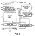
- Fig. 6 is a block diagram of a nonvolatile memory integrated circuit, for example, an EPROM integrated circuit, to which the present invention is applied.
- reference numeral 61 denotes an address buffer to which address data is applied, 62 an address decoder, 63 a memory cell array, 64 a sense amplifier, 65 an input/output buffer, 66 a read/write control circuit, 67 such a charge pump circuit-voltage regulator circuit as shown in Fig. 1, 68 a row drive voltage generator, and 69 a column drive voltage generator.
- Sense amplifier 64 is enabled by a read control signal READ from read/write control circuit 66. When supplied with the enable signal EN from read/write control circuit 66, charge pump circuit-voltage regulator circuit 67 produces a boosted voltage Vout regulated to a substantially constant level.
- Row drive voltage generator 68 applies the boosted voltage Vout from charge pump circuit-voltage regulator circuit 67 to a selected word line of memory cell array 63 in a write mode in which the generator 68 receives a write control signal WRITE from read/write control circuit 66.
- column drive voltage generator 69 is responsive to the write control signal WRITE from read/write control circuit 66 to apply the boosted voltage Vout from charge pump circuit-voltage regulator circuit 67 to a selected column line of memory cell array 63 according to input data from input/output buffer 65.
- the high boosted voltage Vout is applied to the gate and drain of a memory cell connected to the selected word line and column line of memory cell array 63 so that input data is written into the selected memory cell.
- the voltage regulator circuit of the present invention may be applied to E2PROM integrated circuits and logic integrated circuits incorporating nonvolatile memory cells.
Landscapes
- Engineering & Computer Science (AREA)
- Power Engineering (AREA)
- Physics & Mathematics (AREA)
- Microelectronics & Electronic Packaging (AREA)
- Nonlinear Science (AREA)
- Electromagnetism (AREA)
- General Physics & Mathematics (AREA)
- Radar, Positioning & Navigation (AREA)
- Automation & Control Theory (AREA)
- Semiconductor Integrated Circuits (AREA)
- Dram (AREA)
- Dc-Dc Converters (AREA)
Applications Claiming Priority (2)
| Application Number | Priority Date | Filing Date | Title |
|---|---|---|---|
| JP36479/89 | 1989-02-16 | ||
| JP1036479A JPH02215154A (ja) | 1989-02-16 | 1989-02-16 | 電圧制御回路 |
Publications (3)
| Publication Number | Publication Date |
|---|---|
| EP0382929A2 true EP0382929A2 (de) | 1990-08-22 |
| EP0382929A3 EP0382929A3 (en) | 1990-09-26 |
| EP0382929B1 EP0382929B1 (de) | 1994-08-31 |
Family
ID=12470952
Family Applications (1)
| Application Number | Title | Priority Date | Filing Date |
|---|---|---|---|
| EP89123228A Expired - Lifetime EP0382929B1 (de) | 1989-02-16 | 1989-12-15 | Spannungsreglerschaltung |
Country Status (5)
| Country | Link |
|---|---|
| US (1) | US5029282A (de) |
| EP (1) | EP0382929B1 (de) |
| JP (1) | JPH02215154A (de) |
| KR (1) | KR940001251B1 (de) |
| DE (1) | DE68917900T2 (de) |
Cited By (15)
| Publication number | Priority date | Publication date | Assignee | Title |
|---|---|---|---|---|
| FR2681180A1 (fr) * | 1991-09-05 | 1993-03-12 | Gemplus Card Int | Circuit de regulation de tension de programmation, pour memoires programmables. |
| EP0674252A1 (de) * | 1994-03-25 | 1995-09-27 | C.S.E.M. Centre Suisse D'electronique Et De Microtechnique Sa | Schaltung zur Steuerung von Spannungen zwischen Wanne und Source von Transistoren einer logischen MOS-Schaltung und Servosystem zu seiner Leistungsversorgung |
| EP0678802A1 (de) * | 1994-04-21 | 1995-10-25 | STMicroelectronics S.A. | Schaltungsanordnung zur Spannungsbegrenzung mit Hysteresiskomparator |
| EP0737643A1 (de) * | 1995-04-14 | 1996-10-16 | STMicroelectronics S.r.l. | Spannungserhöhungsschaltung zur Erzeugung eines annähernd konstanten Spannungspegels |
| WO1997040574A1 (en) * | 1996-04-25 | 1997-10-30 | Programmable Microelectronics Corporation | Charge pump |
| US5907484A (en) * | 1996-04-25 | 1999-05-25 | Programmable Microelectronics Corp. | Charge pump |
| RU2211478C2 (ru) * | 2001-04-25 | 2003-08-27 | Федеральный научно-производственный центр закрытое акционерное общество "Научно-производственный концерн (объединение) "ЭНЕРГИЯ" | Автономная система электропитания |
| WO2006020296A3 (en) * | 2004-07-26 | 2006-06-15 | Honeywell Int Inc | Precision, low drift, stacked voltage reference |
| WO2009076137A1 (en) * | 2007-12-12 | 2009-06-18 | Sandisk Corporation | Diode connected regulation of charge pumps |
| US7683700B2 (en) | 2008-06-25 | 2010-03-23 | Sandisk Corporation | Techniques of ripple reduction for charge pumps |
| US7795952B2 (en) | 2008-12-17 | 2010-09-14 | Sandisk Corporation | Regulation of recovery rates in charge pumps |
| US9520776B1 (en) | 2015-09-18 | 2016-12-13 | Sandisk Technologies Llc | Selective body bias for charge pump transfer switches |
| US9647536B2 (en) | 2015-07-28 | 2017-05-09 | Sandisk Technologies Llc | High voltage generation using low voltage devices |
| US9917507B2 (en) | 2015-05-28 | 2018-03-13 | Sandisk Technologies Llc | Dynamic clock period modulation scheme for variable charge pump load currents |
| US10060957B2 (en) | 2010-07-29 | 2018-08-28 | Power Monitors, Inc. | Method and apparatus for a cloud-based power quality monitor |
Families Citing this family (70)
| Publication number | Priority date | Publication date | Assignee | Title |
|---|---|---|---|---|
| JPH0470204A (ja) * | 1990-07-11 | 1992-03-05 | Sony Corp | バイアス電圧発生回路及び演算増幅器 |
| JPH04205994A (ja) * | 1990-11-30 | 1992-07-28 | Toshiba Corp | プリチャージ回路 |
| US5126590A (en) * | 1991-06-17 | 1992-06-30 | Micron Technology, Inc. | High efficiency charge pump |
| DE4130191C2 (de) * | 1991-09-30 | 1993-10-21 | Samsung Electronics Co Ltd | Konstantspannungsgenerator für eine Halbleitereinrichtung mit kaskadierter Auflade- bzw. Entladeschaltung |
| KR940005691B1 (ko) * | 1991-10-25 | 1994-06-22 | 삼성전자 주식회사 | 기판전압 발생 장치의 차아지 펌프회로 |
| CN1075690C (zh) * | 1991-11-07 | 2001-11-28 | 摩托罗拉公司 | 混合信号处理系统及其供电方法 |
| EP0954102A1 (de) * | 1991-12-09 | 1999-11-03 | Fujitsu Limited | Exklusiv-NOR-Gatter |
| US5260646A (en) * | 1991-12-23 | 1993-11-09 | Micron Technology, Inc. | Low power regulator for a voltage generator circuit |
| US5191232A (en) * | 1992-03-17 | 1993-03-02 | Silicon Storage Technology, Inc. | High frequency voltage multiplier for an electrically erasable and programmable memory device |
| US5291446A (en) * | 1992-10-22 | 1994-03-01 | Advanced Micro Devices, Inc. | VPP power supply having a regulator circuit for controlling a regulated positive potential |
| JP3420606B2 (ja) * | 1993-03-15 | 2003-06-30 | 株式会社東芝 | 高電圧発生装置 |
| JP3043201B2 (ja) * | 1993-04-22 | 2000-05-22 | 株式会社東芝 | 昇圧回路 |
| US5811990A (en) * | 1993-10-15 | 1998-09-22 | Micron Technology, Inc. | Voltage pump and a level translator circuit |
| US5642073A (en) | 1993-12-06 | 1997-06-24 | Micron Technology, Inc. | System powered with inter-coupled charge pumps |
| JP3159586B2 (ja) * | 1993-12-09 | 2001-04-23 | 株式会社東芝 | 昇圧回路装置 |
| TW271011B (de) * | 1994-04-20 | 1996-02-21 | Nippon Steel Corp | |
| US6140861A (en) * | 1994-06-27 | 2000-10-31 | Texas Instruments Incorporated | Bias pump arrangement including a signal-transition-detection circuit |
| US5513225A (en) * | 1994-08-31 | 1996-04-30 | International Business Machines Corporation | Resistorless phase locked loop circuit employing direct current injection |
| US5491439A (en) * | 1994-08-31 | 1996-02-13 | International Business Machines Corporation | Method and apparatus for reducing jitter in a phase locked loop circuit |
| US5495207A (en) * | 1994-08-31 | 1996-02-27 | International Business Machines Corporation | Differential current controlled oscillator with variable load |
| US5619161A (en) * | 1994-08-31 | 1997-04-08 | International Business Machines Corporation | Diffrential charge pump with integrated common mode control |
| US5525932A (en) * | 1994-08-31 | 1996-06-11 | International Business Machines Corporation | Lock indicator for phase locked loop circuit |
| JP2718375B2 (ja) * | 1994-09-30 | 1998-02-25 | 日本電気株式会社 | チャージポンプ回路 |
| US5694074A (en) * | 1994-10-31 | 1997-12-02 | Mitsubishi Denki Kabushiki Kaisha | Semiconductor integrated circuit being able to generate sufficient boost potential disregarding generation of noise |
| US5541551A (en) * | 1994-12-23 | 1996-07-30 | Advinced Micro Devices, Inc. | Analog voltage reference generator system |
| KR0149220B1 (ko) * | 1994-12-27 | 1998-12-01 | 김주용 | 챠지 펌프 회로 |
| FR2729014A1 (fr) * | 1994-12-29 | 1996-07-05 | Gec Alsthom Transport Sa | Dispositif electronique de conversion de l'energie electrique et installation d'alimentation en faisant usage |
| US5973956A (en) * | 1995-07-31 | 1999-10-26 | Information Storage Devices, Inc. | Non-volatile electrically alterable semiconductor memory for analog and digital storage |
| US5994948A (en) * | 1997-08-27 | 1999-11-30 | Sgs-Thomson Microelectronics S.R.L. | CMOS twin-tub negative voltage switching architecture |
| US6275097B1 (en) | 1999-04-02 | 2001-08-14 | S3 Incorporated, Inc. | Differential charge pump with low voltage common mode feedback circuit |
| US6636104B2 (en) * | 2000-06-13 | 2003-10-21 | Microsemi Corporation | Multiple output charge pump |
| US6556067B2 (en) * | 2000-06-13 | 2003-04-29 | Linfinity Microelectronics | Charge pump regulator with load current control |
| US7467379B2 (en) * | 2001-01-16 | 2008-12-16 | International Business Machines Corporation | System and method for incrementally executing a client/server application |
| US7057511B2 (en) | 2001-02-12 | 2006-06-06 | Symbol Technologies, Inc. | Method, system, and apparatus for communicating with a RFID tag population |
| US6804502B2 (en) | 2001-10-10 | 2004-10-12 | Peregrine Semiconductor Corporation | Switch circuit and method of switching radio frequency signals |
| US6720822B2 (en) * | 2001-10-31 | 2004-04-13 | Stmicroelectronics S.R.L. | Negative charge pump architecture with self-generated boosted phases |
| DE10157865A1 (de) * | 2001-11-26 | 2003-06-26 | Infineon Technologies Ag | Programmierbare Spannungspumpe mit Masse-Option |
| US6498737B1 (en) * | 2002-01-16 | 2002-12-24 | Taiwan Semiconductor Manufacturing Company | Voltage regulator with low sensitivity to body effect |
| US6788130B2 (en) * | 2002-09-25 | 2004-09-07 | Texas Instruments Incorporated | Efficient charge pump capable of high voltage operation |
| US7719343B2 (en) | 2003-09-08 | 2010-05-18 | Peregrine Semiconductor Corporation | Low noise charge pump method and apparatus |
| US7649402B1 (en) * | 2003-12-23 | 2010-01-19 | Tien-Min Chen | Feedback-controlled body-bias voltage source |
| US7119604B2 (en) * | 2004-06-17 | 2006-10-10 | Taiwan Semiconductor Manufacturing Company, Ltd. | Back-bias voltage regulator having temperature and process variation compensation and related method of regulating a back-bias voltage |
| JP4659826B2 (ja) | 2004-06-23 | 2011-03-30 | ペレグリン セミコンダクター コーポレーション | Rfフロントエンド集積回路 |
| FR2878986B1 (fr) * | 2004-12-08 | 2007-04-27 | Atmel Corp | Principe de regulation de puissance d'une sortie a haute tension dans des dispositifs de circuits integres |
| JP2006311731A (ja) * | 2005-04-28 | 2006-11-09 | Seiko Instruments Inc | 電子回路 |
| USRE48965E1 (en) | 2005-07-11 | 2022-03-08 | Psemi Corporation | Method and apparatus improving gate oxide reliability by controlling accumulated charge |
| US20080076371A1 (en) | 2005-07-11 | 2008-03-27 | Alexander Dribinsky | Circuit and method for controlling charge injection in radio frequency switches |
| US7890891B2 (en) | 2005-07-11 | 2011-02-15 | Peregrine Semiconductor Corporation | Method and apparatus improving gate oxide reliability by controlling accumulated charge |
| US9653601B2 (en) | 2005-07-11 | 2017-05-16 | Peregrine Semiconductor Corporation | Method and apparatus for use in improving linearity of MOSFETs using an accumulated charge sink-harmonic wrinkle reduction |
| US7910993B2 (en) | 2005-07-11 | 2011-03-22 | Peregrine Semiconductor Corporation | Method and apparatus for use in improving linearity of MOSFET's using an accumulated charge sink |
| US20070126494A1 (en) * | 2005-12-06 | 2007-06-07 | Sandisk Corporation | Charge pump having shunt diode for improved operating efficiency |
| US7372320B2 (en) * | 2005-12-16 | 2008-05-13 | Sandisk Corporation | Voltage regulation with active supplemental current for output stabilization |
| US20070139099A1 (en) * | 2005-12-16 | 2007-06-21 | Sandisk Corporation | Charge pump regulation control for improved power efficiency |
| US20070229149A1 (en) * | 2006-03-30 | 2007-10-04 | Sandisk Corporation | Voltage regulator having high voltage protection |
| US7554311B2 (en) * | 2006-07-31 | 2009-06-30 | Sandisk Corporation | Hybrid charge pump regulation |
| US7368979B2 (en) | 2006-09-19 | 2008-05-06 | Sandisk Corporation | Implementation of output floating scheme for hv charge pumps |
| CN104282086A (zh) | 2007-01-09 | 2015-01-14 | 功率监视器公司 | 用于智能电路断路器的方法和设备 |
| US7960772B2 (en) | 2007-04-26 | 2011-06-14 | Peregrine Semiconductor Corporation | Tuning capacitance to enhance FET stack voltage withstand |
| DE102007023652B4 (de) * | 2007-05-22 | 2013-08-14 | Austriamicrosystems Ag | Spannungsregler und Verfahren zur Spannungsregelung |
| US8169081B1 (en) | 2007-12-27 | 2012-05-01 | Volterra Semiconductor Corporation | Conductive routings in integrated circuits using under bump metallization |
| WO2009111386A2 (en) | 2008-03-04 | 2009-09-11 | Power Monitors, Inc. | Method and apparatus for a voice-prompted electrical hookup |
| US9660590B2 (en) | 2008-07-18 | 2017-05-23 | Peregrine Semiconductor Corporation | Low-noise high efficiency bias generation circuits and method |
| EP2330735A3 (de) * | 2008-07-18 | 2012-04-04 | Peregrine Semiconductor Corporation | Transkonduktanz-Operationsverstärker |
| JP5259505B2 (ja) * | 2009-06-26 | 2013-08-07 | 株式会社東芝 | 半導体記憶装置 |
| US8773108B2 (en) | 2009-11-10 | 2014-07-08 | Power Monitors, Inc. | System, method, and apparatus for a safe powerline communications instrumentation front-end |
| EP2413105B1 (de) | 2010-07-29 | 2017-07-05 | Power Monitors, Inc. | Verfahren und Vorrichtung für ein Nachfragemanagement-Überwachungssystem |
| US8686787B2 (en) | 2011-05-11 | 2014-04-01 | Peregrine Semiconductor Corporation | High voltage ring pump with inverter stages and voltage boosting stages |
| US9264053B2 (en) | 2011-01-18 | 2016-02-16 | Peregrine Semiconductor Corporation | Variable frequency charge pump |
| US20150236748A1 (en) | 2013-03-14 | 2015-08-20 | Peregrine Semiconductor Corporation | Devices and Methods for Duplexer Loss Reduction |
| CN105404346B (zh) * | 2015-12-22 | 2017-08-08 | 上海华虹宏力半导体制造有限公司 | 电压调整、高压产生和存储器电路 |
Family Cites Families (13)
| Publication number | Priority date | Publication date | Assignee | Title |
|---|---|---|---|---|
| JPS5421249A (en) * | 1977-07-19 | 1979-02-17 | Mitsubishi Electric Corp | Logic circuit |
| JPS5434044A (en) * | 1977-08-19 | 1979-03-13 | Seiko Instr & Electronics Ltd | Constant voltage circuit |
| JPS5632758A (en) * | 1979-08-27 | 1981-04-02 | Fujitsu Ltd | Substrate bias generating circuit |
| JPS5717227A (en) * | 1980-07-04 | 1982-01-28 | Hitachi Ltd | Integrated circuit device |
| US4439692A (en) * | 1981-12-07 | 1984-03-27 | Signetics Corporation | Feedback-controlled substrate bias generator |
| US4553047A (en) * | 1983-01-06 | 1985-11-12 | International Business Machines Corporation | Regulator for substrate voltage generator |
| US4631421A (en) * | 1984-08-14 | 1986-12-23 | Texas Instruments | CMOS substrate bias generator |
| JPS6159688A (ja) * | 1984-08-31 | 1986-03-27 | Hitachi Ltd | 半導体集積回路装置 |
| JPS6212148A (ja) * | 1985-07-10 | 1987-01-21 | Fujitsu Ltd | 半導体集積回路装置 |
| JPS62188255A (ja) * | 1986-02-13 | 1987-08-17 | Toshiba Corp | 基準電圧発生回路 |
| KR890005159B1 (ko) * | 1987-04-30 | 1989-12-14 | 삼성전자 주식회사 | 백 바이어스 전압 발생기 |
| US4837459A (en) * | 1987-07-13 | 1989-06-06 | International Business Machines Corp. | CMOS reference voltage generation |
| US4961167A (en) * | 1988-08-26 | 1990-10-02 | Mitsubishi Denki Kabushiki Kaisha | Substrate bias generator in a dynamic random access memory with auto/self refresh functions and a method of generating a substrate bias therein |
-
1989
- 1989-02-16 JP JP1036479A patent/JPH02215154A/ja active Pending
- 1989-12-14 US US07/450,569 patent/US5029282A/en not_active Expired - Lifetime
- 1989-12-15 EP EP89123228A patent/EP0382929B1/de not_active Expired - Lifetime
- 1989-12-15 DE DE68917900T patent/DE68917900T2/de not_active Expired - Fee Related
-
1990
- 1990-02-16 KR KR1019900001909A patent/KR940001251B1/ko not_active Expired - Fee Related
Cited By (24)
| Publication number | Priority date | Publication date | Assignee | Title |
|---|---|---|---|---|
| WO1993005513A1 (fr) * | 1991-09-05 | 1993-03-18 | Gemplus Card International | Circuit de regulation de tension de programmation, pour memoires programmables |
| FR2681180A1 (fr) * | 1991-09-05 | 1993-03-12 | Gemplus Card Int | Circuit de regulation de tension de programmation, pour memoires programmables. |
| EP0674252A1 (de) * | 1994-03-25 | 1995-09-27 | C.S.E.M. Centre Suisse D'electronique Et De Microtechnique Sa | Schaltung zur Steuerung von Spannungen zwischen Wanne und Source von Transistoren einer logischen MOS-Schaltung und Servosystem zu seiner Leistungsversorgung |
| FR2717918A1 (fr) * | 1994-03-25 | 1995-09-29 | Suisse Electronique Microtech | Circuit pour contrôler les tensions entre caisson et sources des transistors mos et système d'asservissement du rapport entre les courants dynamique et statique d'un circuit logique mos. |
| US5682118A (en) * | 1994-03-25 | 1997-10-28 | C.S.E.M. Centre Suisse D'electronique Et De Microtechnique S.A. | Circuit for controlling the voltages between well and sources of the transistors of and MOS logic circuit, and system for slaving the power supply to the latter including the application thereof |
| US5796285A (en) * | 1994-04-21 | 1998-08-18 | Sgs-Thompson Microelectronics S.A. | Voltage-limiting circuit with hysteresis comparator |
| EP0678802A1 (de) * | 1994-04-21 | 1995-10-25 | STMicroelectronics S.A. | Schaltungsanordnung zur Spannungsbegrenzung mit Hysteresiskomparator |
| FR2719135A1 (fr) * | 1994-04-21 | 1995-10-27 | Sgs Thomson Microelectronics | Circuit de limitation de tension avec comparateur à hystérésis. |
| US5640118A (en) * | 1994-04-21 | 1997-06-17 | Sgs-Thomson Microelectronics S.A. | Voltage-limiting circuit with hysteresis comparator |
| US5914867A (en) * | 1995-04-14 | 1999-06-22 | Sgs-Thomson Microelectronics S.R.L. | Voltage generator-booster for supplying a pulsating voltage having approximately constant voltage levels |
| EP0737643A1 (de) * | 1995-04-14 | 1996-10-16 | STMicroelectronics S.r.l. | Spannungserhöhungsschaltung zur Erzeugung eines annähernd konstanten Spannungspegels |
| WO1997040574A1 (en) * | 1996-04-25 | 1997-10-30 | Programmable Microelectronics Corporation | Charge pump |
| US5907484A (en) * | 1996-04-25 | 1999-05-25 | Programmable Microelectronics Corp. | Charge pump |
| RU2211478C2 (ru) * | 2001-04-25 | 2003-08-27 | Федеральный научно-производственный центр закрытое акционерное общество "Научно-производственный концерн (объединение) "ЭНЕРГИЯ" | Автономная система электропитания |
| WO2006020296A3 (en) * | 2004-07-26 | 2006-06-15 | Honeywell Int Inc | Precision, low drift, stacked voltage reference |
| US7372318B2 (en) | 2004-07-26 | 2008-05-13 | Honeywell International Inc. | Precision, low drift, stacked voltage reference |
| WO2009076137A1 (en) * | 2007-12-12 | 2009-06-18 | Sandisk Corporation | Diode connected regulation of charge pumps |
| US7586363B2 (en) | 2007-12-12 | 2009-09-08 | Sandisk Corporation | Diode connected regulation of charge pumps |
| US7683700B2 (en) | 2008-06-25 | 2010-03-23 | Sandisk Corporation | Techniques of ripple reduction for charge pumps |
| US7795952B2 (en) | 2008-12-17 | 2010-09-14 | Sandisk Corporation | Regulation of recovery rates in charge pumps |
| US10060957B2 (en) | 2010-07-29 | 2018-08-28 | Power Monitors, Inc. | Method and apparatus for a cloud-based power quality monitor |
| US9917507B2 (en) | 2015-05-28 | 2018-03-13 | Sandisk Technologies Llc | Dynamic clock period modulation scheme for variable charge pump load currents |
| US9647536B2 (en) | 2015-07-28 | 2017-05-09 | Sandisk Technologies Llc | High voltage generation using low voltage devices |
| US9520776B1 (en) | 2015-09-18 | 2016-12-13 | Sandisk Technologies Llc | Selective body bias for charge pump transfer switches |
Also Published As
| Publication number | Publication date |
|---|---|
| JPH02215154A (ja) | 1990-08-28 |
| KR900013380A (ko) | 1990-09-05 |
| EP0382929B1 (de) | 1994-08-31 |
| US5029282A (en) | 1991-07-02 |
| DE68917900D1 (de) | 1994-10-06 |
| EP0382929A3 (en) | 1990-09-26 |
| DE68917900T2 (de) | 1995-02-02 |
| KR940001251B1 (ko) | 1994-02-18 |
Similar Documents
| Publication | Publication Date | Title |
|---|---|---|
| EP0382929A2 (de) | Spannungsreglerschaltung | |
| US6041011A (en) | Booster circuit and semiconductor memory device having the same | |
| KR100427739B1 (ko) | 전원 회로 및 그 전원 회로를 구비한 반도체 기억 장치 | |
| KR960002826B1 (ko) | 챠지펌핑효율이 개선된 챠지펌프회로 | |
| US4967399A (en) | Erasable and programmable read-only memory system | |
| KR100254079B1 (ko) | 중간 전압 발생 회로 및 이것을 갖는 불휘발성 반도체 메모리 | |
| KR0155078B1 (ko) | 강전계용의 mos 회로를 갖춘 반도체 회로 | |
| US4704547A (en) | IGFET gating circuit having reduced electric field degradation | |
| US4874967A (en) | Low power voltage clamp circuit | |
| JPH0143464B2 (de) | ||
| US6266276B1 (en) | Non-volatile semiconductor memory device and internal operation method for said non-volatile semiconductor memory device | |
| KR940003409B1 (ko) | 반도체 메모리 장치의 센스앰프 제어회로 | |
| JPH0793022B2 (ja) | 半導体メモリ集積回路 | |
| KR100493599B1 (ko) | 워드선활성화전압의안정화회로를가지는반도체기억장치 | |
| US5631867A (en) | Semiconductor storage device requiring short time for program voltage to rise | |
| US6100744A (en) | Integrated circuit devices having improved internal voltage generators which reduce timing skew in buffer circuits therein | |
| US6735119B2 (en) | Nonvolatile semiconductor memory | |
| US5786719A (en) | Mode setting circuit and mode setting apparatus used to select a particular semiconductor function | |
| JP3392497B2 (ja) | テスト電位転送回路およびこれを用いた半導体記憶装置 | |
| KR100296612B1 (ko) | 출력버퍼의출력전류를크게할수있는반도체기억장치 | |
| US4716303A (en) | MOS IC pull-up circuit | |
| CA1252520A (en) | High reliability complementary logic | |
| US20020000840A1 (en) | Sense amplifier with extended supply voltage range | |
| KR0170286B1 (ko) | 반도체 메모리장치의 전압 승압회로 | |
| JPH09214316A (ja) | 出力回路、リーク電流を減少させるための回路、トランジスタを選択的にスイッチするための方法および半導体メモリ |
Legal Events
| Date | Code | Title | Description |
|---|---|---|---|
| PUAI | Public reference made under article 153(3) epc to a published international application that has entered the european phase |
Free format text: ORIGINAL CODE: 0009012 |
|
| PUAL | Search report despatched |
Free format text: ORIGINAL CODE: 0009013 |
|
| 17P | Request for examination filed |
Effective date: 19891215 |
|
| AK | Designated contracting states |
Kind code of ref document: A2 Designated state(s): DE FR GB |
|
| AK | Designated contracting states |
Kind code of ref document: A3 Designated state(s): DE FR GB |
|
| 17Q | First examination report despatched |
Effective date: 19930416 |
|
| GRAA | (expected) grant |
Free format text: ORIGINAL CODE: 0009210 |
|
| AK | Designated contracting states |
Kind code of ref document: B1 Designated state(s): DE FR GB |
|
| REF | Corresponds to: |
Ref document number: 68917900 Country of ref document: DE Date of ref document: 19941006 |
|
| ET | Fr: translation filed | ||
| PLBE | No opposition filed within time limit |
Free format text: ORIGINAL CODE: 0009261 |
|
| STAA | Information on the status of an ep patent application or granted ep patent |
Free format text: STATUS: NO OPPOSITION FILED WITHIN TIME LIMIT |
|
| 26N | No opposition filed | ||
| PGFP | Annual fee paid to national office [announced via postgrant information from national office to epo] |
Ref country code: FR Payment date: 19971209 Year of fee payment: 9 |
|
| PGFP | Annual fee paid to national office [announced via postgrant information from national office to epo] |
Ref country code: DE Payment date: 19971222 Year of fee payment: 9 |
|
| REG | Reference to a national code |
Ref country code: GB Ref legal event code: 746 Effective date: 19980929 |
|
| PG25 | Lapsed in a contracting state [announced via postgrant information from national office to epo] |
Ref country code: FR Free format text: LAPSE BECAUSE OF NON-PAYMENT OF DUE FEES Effective date: 19990831 |
|
| REG | Reference to a national code |
Ref country code: FR Ref legal event code: ST |
|
| PG25 | Lapsed in a contracting state [announced via postgrant information from national office to epo] |
Ref country code: DE Free format text: LAPSE BECAUSE OF NON-PAYMENT OF DUE FEES Effective date: 19991001 |
|
| REG | Reference to a national code |
Ref country code: GB Ref legal event code: IF02 |
|
| PGFP | Annual fee paid to national office [announced via postgrant information from national office to epo] |
Ref country code: GB Payment date: 20061213 Year of fee payment: 18 |
|
| GBPC | Gb: european patent ceased through non-payment of renewal fee |
Effective date: 20071215 |
|
| PG25 | Lapsed in a contracting state [announced via postgrant information from national office to epo] |
Ref country code: GB Free format text: LAPSE BECAUSE OF NON-PAYMENT OF DUE FEES Effective date: 20071215 |