EP0383326A2 - Digitaler Fir-Filter für Hochgeschwindigkeits-Kommunikationssysteme - Google Patents
Digitaler Fir-Filter für Hochgeschwindigkeits-Kommunikationssysteme Download PDFInfo
- Publication number
- EP0383326A2 EP0383326A2 EP90102963A EP90102963A EP0383326A2 EP 0383326 A2 EP0383326 A2 EP 0383326A2 EP 90102963 A EP90102963 A EP 90102963A EP 90102963 A EP90102963 A EP 90102963A EP 0383326 A2 EP0383326 A2 EP 0383326A2
- Authority
- EP
- European Patent Office
- Prior art keywords
- digital
- output
- samples
- delay
- tap weight
- Prior art date
- Legal status (The legal status is an assumption and is not a legal conclusion. Google has not performed a legal analysis and makes no representation as to the accuracy of the status listed.)
- Granted
Links
Images


Classifications
-
- H—ELECTRICITY
- H03—ELECTRONIC CIRCUITRY
- H03H—IMPEDANCE NETWORKS, e.g. RESONANT CIRCUITS; RESONATORS
- H03H17/00—Networks using digital techniques
- H03H17/02—Frequency selective networks
- H03H17/06—Non-recursive filters
Definitions
- the present invention relates generally to digital filters, and more specifically to a high-speed digital filter suitable for digital radio transmission systems.
- Digital filters are of two types, i.e., IIR (infinite impulse response) filter and FIR (finite impulse response) filter.
- IIR infinite impulse response
- FIR finite impulse response
- the shift registers that comprise a digital filter are the primary source of aliasing, or fold-over distortion noise, they are clocked at twice the symbol rate for oversampling the incoming signal. The clock rate of the shift registers thus determines the maximum operating speed of a digital filter. If higher transmission speed is desired for a system, the clock rate of the digital filters must be increased. However, the operating speed of a digital filter is limited to the maximum operating speed of the integrated circuit components that comprise the shift registers and other constituent parts of the filter.
- a finite impulse response digital filter for a digital communications system.
- the filter has (2n+1) successive virtual taps respectively having tap weight coefficients c j , where n is equal to or greater than 2 and j is in the range between 1 and 2n+1.
- the add-and-delay multiplier circuit comprises a plurality of tap weight multipliers, and a plurality of delay elements connected to the multipliers to define the physical taps, and a plurality of adders.
- a second delay-and-adder circuit which comprises a series of alternately series-connected delaying and summing elements, each of the delaying elements delaying each of the weighted output digital samples for interval T to produce successively delayed samples, and each of the last-mentioned summing elements summing the outputs of the multipliers and the last-mentioned delaying elements to produce a second group of output digital samples d k+1 ⁇ a i-k , d k ⁇ a i-(k-1) , owing d2 ⁇ a i-1 and d1 ⁇ a i as the second output sequence.
- j is in the range between 1 and 2n+1 for coefficients "c” and between 1 and 2m+1 for coefficients "d"
- the odd-numbered output digital samples can be represented by d j ⁇ a i + d j+1 ⁇ a i+1 + ⁇ + d 2m+1 ⁇ a 2m+1 and the even-numbered output digital sample is represented by d 2m+1 ⁇ a i + d 2m ⁇ a i+1 + ⁇ + d j+1 ⁇ a 2m + d j ⁇ a 2m+1 .
- the output of the digital filter is divided into first and second groups.
- first group output samples are sequentially multiplied by tap weights d1, d2 and d3 according to their order of occurrence
- second group output samples are sequentially multiplied by the tap weights in sequence which is opposite to the order of occurrence of the first group.
- An input digital sample a i at symbol rate f s is applied to an input terminal 10 to which are connected the input terminals of tap weight multipliers 1, 2 and 3 having tap weight coefficients d1, d2 and d3, respectively.
- first and second delay-and-adder circuits are provided.
- the first delay-and-adder circuit comprises a shift register 4, an adder 5, a shift register 6 and an adder 7.
- the output terminal of multiplier 1 is connected to the input of shift register 4 and to an input terminal of adder 11.
- Shift register 4 delays the input digital sample for a duration T equal to the reciprocal of the symbol rate f s and produces a digital output sample d1 ⁇ a i-1 which is supplied to an input of adder 5 to which the output of multiplier 2 is supplied. Therefore, adder 5 produces an output sample d1 ⁇ a i-1 + d2 ⁇ a i which is applied to and delayed for interval T by shift register 6 for introduction of a further delay, producing an output sample represented by d1 ⁇ a i-2 + d2 ⁇ a i-1 .
- Adder 7 sums the output of shift register 6 with the output of multiplier 3, generating an output A i represented by a sum of samples d1 ⁇ a i-2 + d2 ⁇ a i-1 + d3 ⁇ a i at one input of a switch 12.
- shift register 8 introduces a delay interval T to the output of multiplier 3 and applies a delayed output sample d3 ⁇ a i-1 to adder 9 which sums it with the output of multiplier 2, producing an output d3 ⁇ a i-1 + d2 ⁇ a1 at the input of shift register 10.
- Shift register 10 delays it for an additional interval T, presenting a delayed output sample d3 ⁇ a i-2 + d2 ⁇ a 1-1 which is summed by adder 11 with the output of multiplier 1 to produce an output sequence B i represented by d3 ⁇ a i-2 + d2 ⁇ a i-1 + d1 ⁇ a i at the other input of switch 12.
- the output sequence A i comprises a sum of d1 ⁇ a1, d2 ⁇ a2 and d3 ⁇ a3 and the output sequence B i comprises a sum of d3 ⁇ a1, d2 ⁇ a2 and d1 ⁇ a3.
- the output sequence A i comprises a sum of d1 ⁇ a2, d2 ⁇ a3 and d3 ⁇ a4 and the sequence B i comprises a sum of d3 ⁇ a2, d2 ⁇ a3 and d1 ⁇ a4.
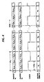
- Fig. 5 is an illustration of a modified form of the digital filter of the invention.
- shift registers 51 and 52 are connected in series from an input terminal 50 to define successive taps to which digital multipliers 53, 54 and 55 of a first set are connected, respectively, and digital multipliers 56 and 57 of a second set are connected to those taps to which multlpliers 53 and 55 are connected.
- Multipliers 53, 54 and 55 have tap weight coefficients d3, d2 and d1, respectively, and multipliers 56 and 57 have coefficients d1 and d3, respectively.
- the outputs of multipliers 53-55 are connected to a first adder 58 to produce the output sequence A i and the outputs of multipliers 16, 54 and 57 are connected to a second adder 59 to produce the second output sequence B i .
- Successively arriving incoming digital samples at symbol rate f s are therefore delayed by shift registers 51 and 52, producing samples a i , a i-1 and a i-2 which are multiplied respectively by multipliers 53-55, producing a weighted output sample d3 ⁇ a i from multiplier 53, a second output sample d2 ⁇ a i-1 from multiplier 54, and a third output sample d1 ⁇ a i-2 from multiplier 55.
- digital samples a i and a i-Z are further multiplied by multipliers 56 and 57, respectively, producing a first output sample d1 ⁇ a i from multiplier 56, a second output sample d2 ⁇ a i-1 from multiplier 54, and a third output sample d3 ⁇ a i-2 from multiplier 57.
Landscapes
- Physics & Mathematics (AREA)
- Engineering & Computer Science (AREA)
- Computer Hardware Design (AREA)
- Mathematical Physics (AREA)
- Filters That Use Time-Delay Elements (AREA)
- Digital Transmission Methods That Use Modulated Carrier Waves (AREA)
- Cable Transmission Systems, Equalization Of Radio And Reduction Of Echo (AREA)
- Transmission Systems Not Characterized By The Medium Used For Transmission (AREA)
Applications Claiming Priority (2)
| Application Number | Priority Date | Filing Date | Title |
|---|---|---|---|
| JP1037486A JPH0828649B2 (ja) | 1989-02-16 | 1989-02-16 | ディジタルフィルタ |
| JP37486/89 | 1989-02-16 |
Publications (3)
| Publication Number | Publication Date |
|---|---|
| EP0383326A2 true EP0383326A2 (de) | 1990-08-22 |
| EP0383326A3 EP0383326A3 (de) | 1991-01-30 |
| EP0383326B1 EP0383326B1 (de) | 1994-09-07 |
Family
ID=12498851
Family Applications (1)
| Application Number | Title | Priority Date | Filing Date |
|---|---|---|---|
| EP90102963A Expired - Lifetime EP0383326B1 (de) | 1989-02-16 | 1990-02-15 | Digitaler Fir-Filter für Hochgeschwindigkeits-Kommunikationssysteme |
Country Status (5)
| Country | Link |
|---|---|
| US (1) | US5031133A (de) |
| EP (1) | EP0383326B1 (de) |
| JP (1) | JPH0828649B2 (de) |
| AU (1) | AU624682B2 (de) |
| DE (1) | DE69012164T2 (de) |
Cited By (1)
| Publication number | Priority date | Publication date | Assignee | Title |
|---|---|---|---|---|
| EP2608401A1 (de) | 2011-12-21 | 2013-06-26 | EM Microelectronic-Marin SA | Übertragungsschaltkreis für RF-ASK-Signale mit Anpassung der Flanken der Datensignale |
Families Citing this family (21)
| Publication number | Priority date | Publication date | Assignee | Title |
|---|---|---|---|---|
| JPH0828649B2 (ja) | 1989-02-16 | 1996-03-21 | 日本電気株式会社 | ディジタルフィルタ |
| US6693951B1 (en) * | 1990-06-25 | 2004-02-17 | Qualcomm Incorporated | System and method for generating signal waveforms in a CDMA cellular telephone system |
| US5659569A (en) * | 1990-06-25 | 1997-08-19 | Qualcomm Incorporated | Data burst randomizer |
| JP2880580B2 (ja) * | 1991-03-22 | 1999-04-12 | シャープ株式会社 | 非巡回型デジタルフィルター回路 |
| JP3357956B2 (ja) * | 1992-08-06 | 2002-12-16 | 日本電気エンジニアリング株式会社 | 判定帰還形等化器 |
| US5561616A (en) * | 1992-08-13 | 1996-10-01 | Tektronix, Inc. | Fir filter based upon squaring |
| FI96256C (fi) * | 1993-04-05 | 1996-05-27 | Tapio Antero Saramaeki | Menetelmä ja järjestely transponoidussa digitaalisessa FIR-suodattimessa binäärisen sisääntulosignaalin kertomiseksi tappikertoimilla sekä menetelmä transponoidun digitaalisen suodattimen suunnittelemiseksi |
| JP2885121B2 (ja) * | 1995-03-06 | 1999-04-19 | 日本電気株式会社 | ディジタルフィルタ |
| US5923888A (en) * | 1997-12-15 | 1999-07-13 | Benschop; Nico Frits | Multiplier for the multiplication of at least two figures in an original format |
| EP0935342A3 (de) * | 1998-01-15 | 2001-05-16 | Texas Instruments Incorporated | Verbesserungen bei oder in Bezug auf Filtervorrichtungen |
| US6304591B1 (en) * | 1998-07-10 | 2001-10-16 | Aloha Networks, Inc. | Match filter architecture based upon parallel I/O |
| WO2000028663A2 (en) * | 1998-11-09 | 2000-05-18 | Broadcom Corporation | Fir filter structure with low latency for gigabit ethernet applications |
| FR2785747B1 (fr) * | 1998-11-09 | 2004-02-13 | Commissariat Energie Atomique | Filtre numerique a architecture parallele et recepteur de signaux a etalement de spectre utilisant un tel filtre |
| US6233593B1 (en) * | 1998-11-18 | 2001-05-15 | Tektronix, Inc. | Fir filter based upon squaring |
| KR100545609B1 (ko) * | 1998-12-30 | 2006-04-21 | 유티스타콤코리아 유한회사 | 통신 시스템의 변조기내 유한 임펄스 응답 필터 |
| US6624691B1 (en) | 1999-10-04 | 2003-09-23 | Nec Corporation | Demodulator for processing digital signal |
| JP3899966B2 (ja) | 2002-03-14 | 2007-03-28 | 松下電器産業株式会社 | ディジタル信号受信装置 |
| US7277479B2 (en) * | 2003-03-02 | 2007-10-02 | Mediatek Inc. | Reconfigurable fir filter |
| US7606322B2 (en) * | 2004-10-07 | 2009-10-20 | Microelectronics Technology Inc. | Digital pre-distortion technique using nonlinear filters |
| CN101040437B (zh) * | 2004-10-13 | 2010-05-12 | 联发科技股份有限公司 | 用于通信系统的滤波器以及滤波方法 |
| WO2012004392A1 (en) | 2010-07-08 | 2012-01-12 | Dsm Ip Assets B.V. | Ballistic resistant article |
Family Cites Families (10)
| Publication number | Priority date | Publication date | Assignee | Title |
|---|---|---|---|---|
| NL7905577A (nl) * | 1979-07-18 | 1981-01-20 | Philips Nv | Inrichting met een niet-recursieffilter. |
| US4691292A (en) * | 1983-04-13 | 1987-09-01 | Rca Corporation | System for digital multiband filtering |
| EP0137464B1 (de) * | 1983-10-05 | 1991-06-12 | Nec Corporation | Digitale Signalverarbeitungseinrichtung mit einem digitalen Filter |
| DE3345284A1 (de) * | 1983-12-14 | 1985-06-27 | Siemens AG, 1000 Berlin und 8000 München | Verfahren und schaltungsanordnung zur digitalsignalverarbeitung nach art eines vorzugsweise adaptiven transversalfilters |
| US4615026A (en) * | 1984-01-20 | 1986-09-30 | Rca Corporation | Digital FIR filters with enhanced tap weight resolution |
| GB2153618B (en) * | 1984-02-01 | 1987-07-22 | British Broadcasting Corp | Processing of periodic signals |
| JPS61113314A (ja) * | 1984-11-08 | 1986-05-31 | Nec Corp | サンプル値間引きデイジタルフイルタ− |
| GB2181008B (en) * | 1985-09-25 | 1989-09-20 | Sony Corp | Infinite impulse response filters |
| GB2181318B (en) * | 1985-10-04 | 1989-12-28 | Sony Corp | Two-dimensional finite impulse response filters |
| JPH0828649B2 (ja) | 1989-02-16 | 1996-03-21 | 日本電気株式会社 | ディジタルフィルタ |
-
1989
- 1989-02-16 JP JP1037486A patent/JPH0828649B2/ja not_active Expired - Lifetime
-
1990
- 1990-02-15 EP EP90102963A patent/EP0383326B1/de not_active Expired - Lifetime
- 1990-02-15 DE DE69012164T patent/DE69012164T2/de not_active Expired - Lifetime
- 1990-02-16 AU AU49896/90A patent/AU624682B2/en not_active Expired
- 1990-02-16 US US07/480,998 patent/US5031133A/en not_active Expired - Lifetime
Cited By (1)
| Publication number | Priority date | Publication date | Assignee | Title |
|---|---|---|---|---|
| EP2608401A1 (de) | 2011-12-21 | 2013-06-26 | EM Microelectronic-Marin SA | Übertragungsschaltkreis für RF-ASK-Signale mit Anpassung der Flanken der Datensignale |
Also Published As
| Publication number | Publication date |
|---|---|
| EP0383326B1 (de) | 1994-09-07 |
| DE69012164D1 (de) | 1994-10-13 |
| EP0383326A3 (de) | 1991-01-30 |
| JPH02216907A (ja) | 1990-08-29 |
| US5031133A (en) | 1991-07-09 |
| JPH0828649B2 (ja) | 1996-03-21 |
| DE69012164T2 (de) | 1995-02-02 |
| AU624682B2 (en) | 1992-06-18 |
| AU4989690A (en) | 1990-08-23 |
Similar Documents
| Publication | Publication Date | Title |
|---|---|---|
| EP0383326B1 (de) | Digitaler Fir-Filter für Hochgeschwindigkeits-Kommunikationssysteme | |
| US5696708A (en) | Digital filter with decimated frequency response | |
| US5339264A (en) | Symmetric transposed FIR digital filter | |
| JP3089630B2 (ja) | サンプリングレート変換装置 | |
| KR100210730B1 (ko) | 디지탈 보간 회로 | |
| JPH08181573A (ja) | カスケード接続積分器 | |
| US5831879A (en) | Digital transmit filter | |
| GB2214386A (en) | Signal equaliser | |
| JP2779617B2 (ja) | 有限インパルス応答フィルタ | |
| EP0180989B1 (de) | Digitaler Filter zur Änderung der Abtastfrequenz | |
| EP0975091A3 (de) | Digitales Filter | |
| US5005185A (en) | Parallel mode adaptive transversal equalizer for high-speed digital communications system | |
| US4612625A (en) | Decimator employing finite impulse response digital filters | |
| AU724637B2 (en) | Decimation method and decimation filter | |
| JPS60501486A (ja) | フィルタ及びそれを用いるデータ伝送システム | |
| EP0174593B1 (de) | Digitaler Schwingkreis | |
| US5784378A (en) | Method and apparatus for time shaped finite impulse response filter with multiple signal stream capability | |
| JPS6243378B2 (de) | ||
| US5912827A (en) | Digital filter with low rolloff factor | |
| KR960014116B1 (ko) | 입력 가중형 트랜스버설필터 | |
| US5148384A (en) | Signal processing integrated circuit | |
| JPH10509011A (ja) | 改良されたディジタルフィルタ | |
| US5068817A (en) | Non-recursive half-band filter with complex valued coefficients for complex input and output signals | |
| US6025750A (en) | Digital filter with long impulse response | |
| CA1281382C (en) | Non-recursive half-band filter |
Legal Events
| Date | Code | Title | Description |
|---|---|---|---|
| PUAI | Public reference made under article 153(3) epc to a published international application that has entered the european phase |
Free format text: ORIGINAL CODE: 0009012 |
|
| 17P | Request for examination filed |
Effective date: 19900307 |
|
| AK | Designated contracting states |
Kind code of ref document: A2 Designated state(s): DE FR GB |
|
| PUAL | Search report despatched |
Free format text: ORIGINAL CODE: 0009013 |
|
| AK | Designated contracting states |
Kind code of ref document: A3 Designated state(s): DE FR GB |
|
| 17Q | First examination report despatched |
Effective date: 19931122 |
|
| GRAA | (expected) grant |
Free format text: ORIGINAL CODE: 0009210 |
|
| AK | Designated contracting states |
Kind code of ref document: B1 Designated state(s): DE FR GB |
|
| REF | Corresponds to: |
Ref document number: 69012164 Country of ref document: DE Date of ref document: 19941013 |
|
| RAP2 | Party data changed (patent owner data changed or rights of a patent transferred) |
Owner name: NEC CORPORATION |
|
| ET | Fr: translation filed | ||
| PLBE | No opposition filed within time limit |
Free format text: ORIGINAL CODE: 0009261 |
|
| STAA | Information on the status of an ep patent application or granted ep patent |
Free format text: STATUS: NO OPPOSITION FILED WITHIN TIME LIMIT |
|
| 26N | No opposition filed | ||
| REG | Reference to a national code |
Ref country code: GB Ref legal event code: IF02 |
|
| PGFP | Annual fee paid to national office [announced via postgrant information from national office to epo] |
Ref country code: DE Payment date: 20090213 Year of fee payment: 20 |
|
| PGFP | Annual fee paid to national office [announced via postgrant information from national office to epo] |
Ref country code: GB Payment date: 20090211 Year of fee payment: 20 |
|
| PGFP | Annual fee paid to national office [announced via postgrant information from national office to epo] |
Ref country code: FR Payment date: 20090213 Year of fee payment: 20 |
|
| REG | Reference to a national code |
Ref country code: GB Ref legal event code: PE20 Expiry date: 20100214 |
|
| PG25 | Lapsed in a contracting state [announced via postgrant information from national office to epo] |
Ref country code: GB Free format text: LAPSE BECAUSE OF EXPIRATION OF PROTECTION Effective date: 20100214 |
|
| PG25 | Lapsed in a contracting state [announced via postgrant information from national office to epo] |
Ref country code: DE Free format text: LAPSE BECAUSE OF EXPIRATION OF PROTECTION Effective date: 20100215 |