EP0384286B1 - Dispositif à couplage de charge sans image subséquente due à des charges électriques résiduelles - Google Patents
Dispositif à couplage de charge sans image subséquente due à des charges électriques résiduelles Download PDFInfo
- Publication number
- EP0384286B1 EP0384286B1 EP90102894A EP90102894A EP0384286B1 EP 0384286 B1 EP0384286 B1 EP 0384286B1 EP 90102894 A EP90102894 A EP 90102894A EP 90102894 A EP90102894 A EP 90102894A EP 0384286 B1 EP0384286 B1 EP 0384286B1
- Authority
- EP
- European Patent Office
- Prior art keywords
- impurity regions
- transfer gate
- conductivity type
- semiconductor substrate
- charge coupled
- Prior art date
- Legal status (The legal status is an assumption and is not a legal conclusion. Google has not performed a legal analysis and makes no representation as to the accuracy of the status listed.)
- Expired - Lifetime
Links
Images


Classifications
-
- H—ELECTRICITY
- H10—SEMICONDUCTOR DEVICES; ELECTRIC SOLID-STATE DEVICES NOT OTHERWISE PROVIDED FOR
- H10F—INORGANIC SEMICONDUCTOR DEVICES SENSITIVE TO INFRARED RADIATION, LIGHT, ELECTROMAGNETIC RADIATION OF SHORTER WAVELENGTH OR CORPUSCULAR RADIATION
- H10F39/00—Integrated devices, or assemblies of multiple devices, comprising at least one element covered by group H10F30/00, e.g. radiation detectors comprising photodiode arrays
- H10F39/10—Integrated devices
- H10F39/12—Image sensors
- H10F39/15—Charge-coupled device [CCD] image sensors
- H10F39/153—Two-dimensional or three-dimensional array CCD image sensors
Definitions
- This invention relates to a charge coupled device and, more particularly, to the configuration of a photo electric converting element.
- a solid state line sensor is implemented by a charge coupled device and used as an image sensor associated with an automatic focus controlling mechanism of a camera or incorporated in a facsimile machine.
- Fig. 1 shows the layout of a prior art charge coupled device fabricated on a p-type semiconductor substrate 1, and a p-type channel stopper 2 provides an electrical isolation between adjacent photo electric converting elements 3 and 4 and a shift register 5.
- the p-type channel stopper 2 is indicated by hatch lines for better understanding.
- each of the photo-electric converting elements 3 and 4 is implemented by the p-n junction type photo diode, and the photo electric converting element 4 is, by way of example, formed by an n-type impurity region 6 partially overlapped with a p-type impurity region 7.
- the n-type impurity region 6 is reversely biased with respect to the p-type semiconductor substrate 1.
- an n-type impurity region 8 which forms the shift register 5 together with transfer gate electrodes 9, 10, 11 and 12 embedded in an insulating film 13 in a partially overlapping manner.
- the transfer gate electrodes 9 and 10 are supplied with a first phase clock pulse CL1, and a second phase clock pulse CL2 is fed to the transfer gate electrodes 11 and 12.
- the shift register 5 thus arranged transfers a data signal in the form of electric charges in synchronization with the two phase clock signal in the left direction of Fig. 1.
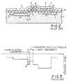
- Photo shield plates 14 and 15 are provided on the insulating film 13 and are spaced from each other for exposing a part of photo electric converting elements 3 and 4 to an optical radiation carrying photo images, and parts of the optical radiation are converted into electric charges the amounts of which are dependent to the respective intensities of the parts of the optical radiation.
- a transfer gate electrode 16 allows the electric charges to flow into the shift register 5.
- the transfer gate electrode 16 is partially overlapped with the n-type impurity region 6 at a overlapping area L encircled by dash lines 17, and the edge of the transfer gate electrode 9 extends below the transfer gate electrode 16.
- the electric charges accumulated in the n-type impurity region 6 are read out to the shift register 5 in the presence of a transfer pulse Pt of a high voltage level fed to the transfer gate electrode 16, and the shift register 5 transfers the electric charges in synchronization with the two phase shift clock signal as described above.
- the residual electric charges may be reduced by decreasing the overlapping area to a certain extent allowed in consideration of a nesting tolerance. However, this approach never satisfies the user.
- the present invention as defined in the claim proposes to decrease the leading end portion of an n-type impurity region in width to a certain extent preventing the n-type impurity region from a narrow channel phenomenon.
- a charge coupled device embodying the present invention largely comprises a photo array 30 having a plurality of photo electric converting elements including elements 31, 32 and 33, a plurality of vertical shift registers including registers 34 and 35 and a horizontal shift register 36, and these components are fabricated on a single semiconductor substrate 37.
- the photo electric converting elements are implemented by p-n junction type diodes, respectively.
- the photo electric converting elements 31 to 33 are coupled to the associated vertical shift registers 34 and 35 through gate transistors 38, 39 and 40, and the vertical shift registers 34 and 35 are in turn coupled to a horizontal shift register 36.
- the photo electric converting elements 31 to 33 When an optical radiation carrying images is fallen upon the photo electric converting elements 31 to 33, the photo electric converting elements 31 to 33 produce electric charges depending upon the intensities of respective parts of the optical radiation, and the electric charges are transferred through the transfer gates to the vertical shift registers 34 and 35 in the presence of a transfer pulse Pt of an active high voltage level.
- the electric charges thus flowing into the vertical shift registers 34 and 35 are conveyed in synchronization with a two phase clock signal consisting of a first phase clock pulse CL1 and a second phase clock pulse CL2.
- the electric charges then flow into the horizontal shift register 36, and are sequentially extracted from the horizontal shift register 36.
- the electric charges thus sequentially extracted from the horizontal shift register 36 are used for reproducing the images on a display unit.
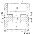
- the charge coupled device according to the present invention is similar to that shown in Fig. 1 with the exception of the configuration of each of the photo electric converting elements 31 to 33, and, for this reason, other elements, regions and films are designated by the same reference numerals used in Fig. 1 without any detailed description, and the heavily doped channel stopper 2 is indicated by hatch lines. All of the photo electric converting elements are identical with one another, so that description is made on the photo electric converting element 31 only with reference to Fig. 5.
- the photo electric converting element 31 has a generally rectangular wide portion 42 and a narrow portion 43 contiguous to the wide portion 43, and the narrow portion 43 extends below the transfer gate electrode 16 of the gate transistor 38.
- the photo electric converting element 31 is implemented by an n-type impurity region 51 contacting a p-type impurity region 52 as similar to the prior art photo electric converting element (see Fig. 6), the p-type impurity region 52 is removed from the leading end sub-portion of the narrow portion 43 overlapped with the transfer gate electrode 16.
- a channel forming area 44 is defined by the channel stopper 2 and is contiguous to the leading end sub-portion of the narrow portion 43.
- the wide portion 42 is about 14 ⁇ m in width (W1), and the narrow portion 43 is as narrow as about 6 ⁇ m (W2).
- the overlapping area (S1) is as large as 28 ⁇ m2 and, accordingly, results in 2.4 x 10³ residual electric charges.
- the narrow portion 43 leads to substantial reduction in the amount of the residual electric charges Qr, and any after image is less liable to take place on the display unit.
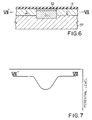
- the p-type channel stopper are formed on both sides of the n-type impurity region 51, and, for this reason, depletion layers extend from the p-n junctions between the n-type impurity region 51 and the p-type channel stopper 2 into the n-type impurity region 51. These depletion layers are causative of lifting the potential edge at the both side portions of the n-type impurity region 51 as shown in Fig. 7.
- Figs. 8(A) to 8(D) show a variety of channel configurations, and W is indicative of the width of an n-type impurity region 71.
- Reference numerals 72, 73 and 74 respectively designate a p-type channel stopper, an insulating film and a conductive film.
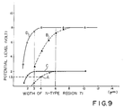
- the narrow portion 43 is of the structure shown in Fig. 8(C), and the potential level in terms of the width W traces Plots A of Fig. 9. In this structure, if the width is decreased to a value less than 6 ⁇ m, the potential level is lowered than that in the wide portion 42, and such a potential gap means a potential barrier between the wide portion 42 and the narrow portion 43 against the electric charges.
- the width W2 of the narrow portion 43 is of the order of 4 ⁇ m, the potential level thereof is about 1.3 volt, and, for this reason, the potential barrier of about 0.7 volt takes place between the wide portion 42 and the narrow portion 43.
- the narrow portion 43 needs to be equal to or greater than about 6 ⁇ m so as to avoid the potential barrier or the narrow channel phenomenon.
- the narrow portion 43 beneath the transfer gate electrode 16 is of the structure shown in Fig. 8(A), and the potential level in terms of the width W is represented by Plots B of Fig. 9. Namely, the leading sub-portion of the narrow portion 43 consists of the n-type impurity region 51 only as shown in Fig. 10.
- Plots B teaches us that potential level L2 at 6 ⁇ m is about 7.5 volts, so that the narrow channel phenomenon takes place in the width W of the order of 6 ⁇ m.
- the narrow portion 43 below the transfer gate electrode 16 merely allows the electric charge to pass therethrough, and the width W2 of the order of 6 ⁇ m is not causative of any problem because the potential level L2 is greater than the potential level L1 of 2 volts in the wide portion 42 (see Fig. 11).
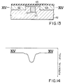
- a photo electric converting element 61 is fabricated on a semiconductor substrate 62 and defined by a p-type channel stopper 63 indicated by hatch lines.
- the photo electric converting element 61 is implemented by an n-type impurity region 64 partially covered with a p-type impurity region 65 as will be seen from Fig. 13, and the n-type impurity region 64 has a generally rectangular wide portion 66 and a narrow portion 67 projecting from the wide portion 66.
- the narrow portion 67 extends under a transfer gate electrode 68 of a gate transistor 69, so that a leading sub-portion of the narrow portion 67 is located under the transfer gate electrode 68, but a boss sub-portion is not overlain by the gate electrode 68.
- the gate transistor 69 provides a bridge between the photo electric converting element 61 and a vertical shift registor (not shown) as similar to the charge coupled device shown in Fig. 4, and the vertical shift register in turn is coupled to a horizontal shift register (not shown).
- the narrow portion 67 is not contiguous to the heavily doped channel stopper 63, but the lightly doped p-type semiconductor substrate 62 intervenes between the channel stopper 63 and the narrow portion 67.
- the photo electric converting element 61 thus arranged is of the structure shown in Fig. 8(D), and the potential level in terms of the width W varies along Plots C of Fig. 9. Comparing Plots A with Plots C, the narrow channel phenomenon is less liable to take place in the n-type impurity region 64 rather than the n-type impurity region 51. This is because of the fact that depletion layers easily extend into the lightly doped semiconductor substrate 62.
- the overlapping area S3 thus reduced results in the residual electric charges of about 3 x 10² which is a eighth of the residual electric charges produced in the prior art charge coupled device. As a result, any after image is effectively eliminated from a display unit.
- the residual electric charges are drastically reduced from the photo electric converting element according to the present invention without any serious problem in the nesting tolerance.
Landscapes
- Solid State Image Pick-Up Elements (AREA)
Claims (1)
- Capteur d'images à couplage de charges formé sur un substrat semi-conducteur légèrement dopé (1) d'un premier type de conductibilité, comprenant : a) une multitude d'éléments de conversion photo-électrique (31) qui sont constitués d'une multitude de premières régions d'impureté (51) d'un second type de conductibilité opposé audit premier type de conductibilité formées dans ledit substrat semi-conducteur, et d'une multitude de secondes régions d'impureté (52) dudit premier type de conductibilité respectivement formées dans ledit substrat semi-conducteur et recouvrant lesdites premières régions d'impureté, sauf les portions d'extrémité avant lesdites premières régions d'impureté de façon à former des jonctions pn, lesdits éléments de conversion photo-électrique formant une multitude de groupes d'éléments ; b) une multitude de registres à décalages verticaux (35) respectivement associés à ladite multitude de groupes d'éléments et comportant des troisièmes régions d'impureté (8) dudit second type de conductibilité ; c) un film isolant (13) recouvrant lesdites première, seconde et troisième régions d'impureté ; et d) : une multitude d'électrodes de grille de transfert (16) prévues entre lesdits éléments de conversion photo-électrique et les registres à décalages verticaux associés, lesdites électrodes de grille de transfert s'étendant respectivement sur des zones formant canal dudit substrat semi-conducteur entre lesdites premières régions d'impureté et lesdites troisièmes régions d'impureté, lesdites portions d'extrémité avant desdites premières régions d'impureté étant placées sous lesdites électrodes de grille de transfert, respectivement, caractérisé en ce que chacune desdites premières régions d'impureté comprend une portion large (42) et une portion étroite (43) contiguë à la portion large, ladite portion étroite ayant une première sous-portion placée dans cette zone non recouverte par ladite électrode de grille de transfert et une sous-portion d'extrémité avant recouverte par ladite électrode de grille de transfert, la largeur de ladite première sous-portion étant plus grande qu'une valeur critique où un phénomène de canal étroit a lieu.
Applications Claiming Priority (2)
| Application Number | Priority Date | Filing Date | Title |
|---|---|---|---|
| JP1040770A JPH02219270A (ja) | 1989-02-20 | 1989-02-20 | 固体撮像装置 |
| JP40770/89 | 1989-02-20 |
Publications (2)
| Publication Number | Publication Date |
|---|---|
| EP0384286A1 EP0384286A1 (fr) | 1990-08-29 |
| EP0384286B1 true EP0384286B1 (fr) | 1994-05-11 |
Family
ID=12589869
Family Applications (1)
| Application Number | Title | Priority Date | Filing Date |
|---|---|---|---|
| EP90102894A Expired - Lifetime EP0384286B1 (fr) | 1989-02-20 | 1990-02-14 | Dispositif à couplage de charge sans image subséquente due à des charges électriques résiduelles |
Country Status (4)
| Country | Link |
|---|---|
| US (1) | US5049960A (fr) |
| EP (1) | EP0384286B1 (fr) |
| JP (1) | JPH02219270A (fr) |
| DE (1) | DE69008749T2 (fr) |
Families Citing this family (6)
| Publication number | Priority date | Publication date | Assignee | Title |
|---|---|---|---|---|
| US5302543A (en) * | 1989-11-06 | 1994-04-12 | Mitsubishi Denki Kabushiki Kaisha | Method of making a charge coupled device |
| US5189498A (en) * | 1989-11-06 | 1993-02-23 | Mitsubishi Denki Kabushiki Kaisha | Charge coupled device |
| JP3125303B2 (ja) * | 1990-11-26 | 2001-01-15 | 日本電気株式会社 | 固体撮像素子 |
| JP3297988B2 (ja) * | 1997-01-24 | 2002-07-02 | シャープ株式会社 | アクティブマトリクス基板 |
| US6476426B1 (en) | 1999-07-06 | 2002-11-05 | Motorola, Inc. | Electronic component and method for improving pixel charge transfer in the electronic component |
| DE102007029898B3 (de) * | 2007-06-28 | 2008-08-21 | MAX-PLANCK-Gesellschaft zur Förderung der Wissenschaften e.V. | Halbleiterdetektor zur Strahlungsdetektion und zugehöriges Betriebsverfahren |
Family Cites Families (9)
| Publication number | Priority date | Publication date | Assignee | Title |
|---|---|---|---|---|
| GB1437328A (en) * | 1972-09-25 | 1976-05-26 | Rca Corp | Sensors having recycling means |
| DE2542156C3 (de) * | 1975-09-22 | 1978-08-03 | Siemens Ag, 1000 Berlin Und 8000 Muenchen | Eindimensionaler optoelektronischer Sensor |
| US4087833A (en) * | 1977-01-03 | 1978-05-02 | Reticon Corporation | Interlaced photodiode array employing analog shift registers |
| DE2813254C2 (de) * | 1978-03-28 | 1979-12-06 | Siemens Ag, 1000 Berlin Und 8000 Muenchen | Eindimensionaler CCD-Sensor mit Überlaufvorrichtung |
| JPS6033345B2 (ja) * | 1979-06-08 | 1985-08-02 | 日本電気株式会社 | 電荷転送撮像装置とその駆動方法 |
| US4484210A (en) * | 1980-09-05 | 1984-11-20 | Nippon Electric Co., Ltd. | Solid-state imaging device having a reduced image lag |
| US4696021A (en) * | 1982-06-03 | 1987-09-22 | Nippon Kogaku K.K. | Solid-state area imaging device having interline transfer CCD means |
| JPS60202961A (ja) * | 1984-03-28 | 1985-10-14 | Hitachi Ltd | 電荷移送型固体撮像素子 |
| JPH0682823B2 (ja) * | 1984-06-27 | 1994-10-19 | 株式会社東芝 | 固体撮像装置 |
-
1989
- 1989-02-20 JP JP1040770A patent/JPH02219270A/ja active Pending
-
1990
- 1990-02-14 EP EP90102894A patent/EP0384286B1/fr not_active Expired - Lifetime
- 1990-02-14 DE DE69008749T patent/DE69008749T2/de not_active Expired - Fee Related
- 1990-02-20 US US07/482,096 patent/US5049960A/en not_active Expired - Lifetime
Also Published As
| Publication number | Publication date |
|---|---|
| EP0384286A1 (fr) | 1990-08-29 |
| DE69008749D1 (de) | 1994-06-16 |
| DE69008749T2 (de) | 1994-08-25 |
| JPH02219270A (ja) | 1990-08-31 |
| US5049960A (en) | 1991-09-17 |
Similar Documents
| Publication | Publication Date | Title |
|---|---|---|
| US4517733A (en) | Process for fabricating thin film image pick-up element | |
| US4236168A (en) | One-dimensional CCD sensor with overflow arrangement | |
| US5477070A (en) | Drive transistor for CCD-type image sensor | |
| US4471371A (en) | Thin film image pickup element | |
| US4878102A (en) | Charge-coupled device | |
| US5256890A (en) | Non-interlacing charge coupled device of a frame interline transfer type | |
| EP0384286B1 (fr) | Dispositif à couplage de charge sans image subséquente due à des charges électriques résiduelles | |
| EP0253330B1 (fr) | Dispositif de prise de vue à l'état solide | |
| EP0383210B1 (fr) | Dispositif à transfert de charge réalisant une grande efficacité de transfert de charge sans sacrifier la dynamique du signal de sortie | |
| US5196719A (en) | Solid-state image pick-up device having electric field for accelerating electric charges from photoelectric converting region to shift register | |
| KR100233185B1 (ko) | 인터라인 전달 ccd 이미지 센서의 화소배열구조를 가진 고체촬상장치 | |
| EP0497326B1 (fr) | Un transducteur photo-électrique commutable en mode haute résolution ou haute sensibilité | |
| KR100525044B1 (ko) | 박막 트랜지스터형 광 감지소자 제조방법 | |
| KR920007785B1 (ko) | 이미지 센서장치 및 그 제조방법 | |
| EP0132870B1 (fr) | Dispositif semi-conducteur sensible à la radiation | |
| EP0457192B1 (fr) | Dispositif capteur d'images à l'état solide comportant un champ électrique pour accélérer les charges électriques venant de la région de conversion photo-électrique vers le registre à décalage | |
| US5289029A (en) | Semiconductor integrated circuit device having wells biased with different voltage levels | |
| US5294817A (en) | Output circuit for charged transfer device and having a high detection sensitivity | |
| EP0457271B1 (fr) | Dispositif de transfert de charges | |
| US5066994A (en) | Image sensor | |
| JPH07114270B2 (ja) | 半導体集積回路装置 | |
| US5005062A (en) | Image sensor device of the frame transfer type | |
| US6310933B1 (en) | Charge transferring device and charge transferring method which can reduce floating diffusion capacitance | |
| JPS6134263B2 (fr) | ||
| JPS6258551B2 (fr) |
Legal Events
| Date | Code | Title | Description |
|---|---|---|---|
| PUAI | Public reference made under article 153(3) epc to a published international application that has entered the european phase |
Free format text: ORIGINAL CODE: 0009012 |
|
| 17P | Request for examination filed |
Effective date: 19900214 |
|
| AK | Designated contracting states |
Kind code of ref document: A1 Designated state(s): DE FR GB |
|
| 17Q | First examination report despatched |
Effective date: 19930914 |
|
| GRAA | (expected) grant |
Free format text: ORIGINAL CODE: 0009210 |
|
| AK | Designated contracting states |
Kind code of ref document: B1 Designated state(s): DE FR GB |
|
| PG25 | Lapsed in a contracting state [announced via postgrant information from national office to epo] |
Ref country code: FR Effective date: 19940511 |
|
| REF | Corresponds to: |
Ref document number: 69008749 Country of ref document: DE Date of ref document: 19940616 |
|
| EN | Fr: translation not filed | ||
| PLBE | No opposition filed within time limit |
Free format text: ORIGINAL CODE: 0009261 |
|
| STAA | Information on the status of an ep patent application or granted ep patent |
Free format text: STATUS: NO OPPOSITION FILED WITHIN TIME LIMIT |
|
| 26N | No opposition filed | ||
| REG | Reference to a national code |
Ref country code: GB Ref legal event code: IF02 |
|
| PGFP | Annual fee paid to national office [announced via postgrant information from national office to epo] |
Ref country code: GB Payment date: 20030212 Year of fee payment: 14 |
|
| PGFP | Annual fee paid to national office [announced via postgrant information from national office to epo] |
Ref country code: DE Payment date: 20030227 Year of fee payment: 14 |
|
| REG | Reference to a national code |
Ref country code: GB Ref legal event code: 732E |
|
| PG25 | Lapsed in a contracting state [announced via postgrant information from national office to epo] |
Ref country code: GB Free format text: LAPSE BECAUSE OF NON-PAYMENT OF DUE FEES Effective date: 20040214 |
|
| PG25 | Lapsed in a contracting state [announced via postgrant information from national office to epo] |
Ref country code: DE Free format text: LAPSE BECAUSE OF NON-PAYMENT OF DUE FEES Effective date: 20040901 |
|
| GBPC | Gb: european patent ceased through non-payment of renewal fee |
Effective date: 20040214 |